


PL_to_PS中断传输数据
实验功能:将PL端的数据存入BRAM,然后在PS端读出数据,用串口打印。通过中断来触发
参考文章:
https://www.cnblogs.com/fhyfhy/p/11760986.html
[ZYNQ_PS与PL通过BRAM交互(三:PSPL读写) - 知乎 (zhihu.com)](https://zhuanlan.zhihu.com/p/661468152)
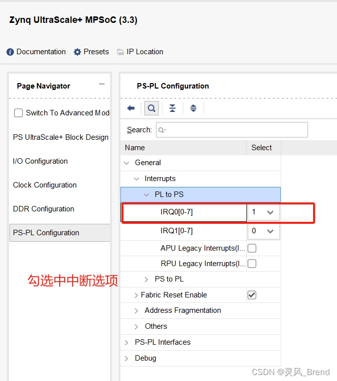
PL的BD配置
ZYNQ勾选上中断
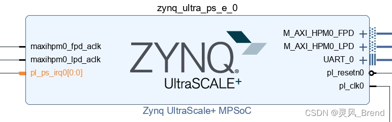
ZYNQ:
BRAM写入数据
我的工程是将ADC采集的数据进行信号处理,然后写入BRAM传输到PS端进行下一步的处理核分析。
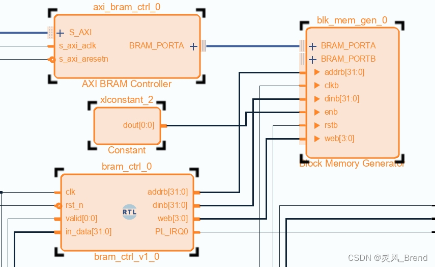
如上图所示,是将数据写入BRAM中的步骤。其中bram_ctrl_0是我自己写的一个模块,它的功能是将数据写入BRAM,并且我加了中断,检测到上升沿启动写过程时,产生一个脉冲中断信号。
bram_ctrl代码如下:
module bram_ctrl(
	input       clk,
	input 		rst_n,
	input		valid,
    input    	[31:0]	in_data,	//写入的数据

	output   	[31:0]	addrb,
	output reg 	[31:0]	dinb ,
	output reg 	[3:0] 	web  ,
	output reg			PL_IRQ0		//脉冲中断信号
	);
/************** 		 **************/
/**************    信号定义      **************/
/************** 		 **************/
	//PL写RAM
	wire [31:0]AddrEndValueVio; //控制写的地址范围
	wire [31:0]dinbValueVio;	//控制写的数据数值
	wire [3:0] webVio;			//控制写的有效字节位
	wire [0:0] valid;		//启动写数据

	reg [0:0]valid1;//对writeEnVio延迟一个clk
	reg [0:0]wrState;    //写数据状态:0代表IDLE.1代表正在写
	reg [31:0]addrbWrite;//写数据地址

	//Ohter signals
	assign    addrb = wrState?addrbWrite:32'd0;
	reg  [0:0]wrStateReg;

/**************			  **************/
/**************    PL 写入BRAM    **************/
/**************			  **************/

always@(posedge clk)begin
	if(!rst_n)begin
		valid1 <= 1'b0;
	end
	else begin
		valid1 <= valid;
	end
end

always@(posedge clk)begin
	if(!rst_n)begin
		dinb[31:0]        <= 32'd0;
		web[3:0]          <=  4'd0;
		wrState           <= 1'b0;
		addrbWrite[31:0]  <= 32'd0;
	end
	else begin
		case(wrState)
		1'b0:
			if(valid&~valid1)begin//边沿检测,检测到上升沿启动写过程
				wrState           <= 1'b1;
				web[3:0]          <= 4'b1111;
				addrbWrite[31:0]  <= 32'd0;
				dinb[31:0]        <= in_data[31:0];
			end else begin
				wrState           <= wrState;
				web[3:0]          <= 4'd0;
				addrbWrite[31:0]  <= 32'd0;
				dinb[31:0]        <= 32'd0;
			end

		1'b1:
			if(addrbWrite[31:0] >= 32'd2012)begin
				wrState[0:0]      <= 1'b0;
				web[3:0]          <= 4'd0;
				addrbWrite[31:0]  <= 32'd0;
				dinb[31:0]        <= 32'd0;
			end
			else begin
				wrState[0:0] <= wrState[0:0];
				web[3:0]     <= 4'b1111;
				addrbWrite[31:0]  <= addrbWrite[31:0] + 32'd4;
				// dinb[31:0]   <= in_data[31:0];//写入每个地址相同数据
				//dinb[31:0]   <= dinb[31:0] + 32'd1;   //写入每个地址数据累加1
				dinb[31:0]   <= dinb[31:0];   //保持
			end
		endcase
	end
end

//中断
always@(posedge clk)begin
	if(!rst_n)begin
		PL_IRQ0 <= 1'b0;
	end
	else if(valid&~valid1) begin
		PL_IRQ0 <= 1'b1;
	end
	else
		PL_IRQ0 <= 1'b0;
end

endmodule
代码解释:一共有三个always语句块。
第一个是将valid寄存一个拍,为了后续的边沿检测。
第二个是数据写入,用了一个状态机。if(valid&~valid1) 当检测到valid的上升沿时,开始写入数据。
第三个是产生一个中断信号PL_IRQ0。由valid的上升沿触发产生。
以上是PL端的工作,下面是PS的工作
PS 代码思路解释
建立项目的模板选用《Hello World》
将主函数修改为:
#include <stdio.h>
#include "platform.h"
#include "xil_printf.h"
#include "xscugic.h"
#include "xil_exception.h"
#include "xparameters.h"
#include "xparameters_ps.h"
#include <xil_io.h>

#define  INTC_DEVICE_ID          XPAR_SCUGIC_0_DEVICE_ID
#define ADC0_BRAM_ADDR       XPAR_ADC0_AXI_BRAM_CTRL_0_S_AXI_BASEADDR
#define ADC1_BRAM_ADDR       XPAR_ADC1_AXI_BRAM_CTRL_0_S_AXI_BASEADDR

static XScuGic INTCInst;

static void SW0_intr_Handler();

static int IntcInitFunction(u16 DeviceId);

// 中断服务函数
void psReadBram()
{
    int ADC0_data;
    int ADC1_data;
    printf("Interrupt detected!\r\n");
    printf("This is psReadBram function\r\n");

    ADC0_data = Xil_In32(ADC0_BRAM_ADDR + 4);
    ADC1_data = Xil_In32(ADC1_BRAM_ADDR + 4);
    printf("ADC0_data:%d \r\n",ADC0_data);
    printf("ADC1_data:%d \r\n",ADC1_data);
}

int IntcInitFunction(u16 DeviceId)
{
    XScuGic_Config *IntcConfig;
    int status;

    // Interrupt controller initialisation
    IntcConfig = XScuGic_LookupConfig(DeviceId);
    status = XScuGic_CfgInitialize(&INTCInst, IntcConfig, IntcConfig->CpuBaseAddress);
    if(status != XST_SUCCESS) return XST_FAILURE;

    // Call to interrupt setup
    Xil_ExceptionRegisterHandler(XIL_EXCEPTION_ID_INT,
                                 (Xil_ExceptionHandler)XScuGic_InterruptHandler,
                                 &INTCInst);
    Xil_ExceptionEnable();

    // Connect PL interrupt to handler
    status = XScuGic_Connect(&INTCInst,
    		                 XPS_FPGA0_INT_ID,
                             (Xil_ExceptionHandler)psReadBram,
                             (void *)1);

    if(status != XST_SUCCESS) return XST_FAILURE;

    // Set interrupt type of PL to rising edge
    XScuGic_SetPriorityTriggerType(&INTCInst, XPS_FPGA0_INT_ID, 0x00, 0x03);

    // Enable PL interrupts in the controller
    XScuGic_Enable(&INTCInst, XPS_FPGA0_INT_ID);

    return XST_SUCCESS;
}


int main()
{
    init_platform();
    IntcInitFunction(INTC_DEVICE_ID);
    RF_init();
    while(1);
    cleanup_platform();
    return 0;
}
代码解释:一个中断函数 IntcInitFunction;一个中断服务函数 psReadBram;一个主函数 main
其中main函数中的 RF_init(); 是我的ADC采集初始化函数。
#define ADC0_BRAM_ADDR       XPAR_ADC0_AXI_BRAM_CTRL_0_S_AXI_BASEADDR
#define ADC1_BRAM_ADDR       XPAR_ADC1_AXI_BRAM_CTRL_0_S_AXI_BASEADDR
这两个宏定义是两个BRAM的地址。(我用了两个ADC,写入两个BRAM中)
在中断服务函数psReadBram中,我将ADC0_BRAM_ADDR + 4 该地址的数据读出来赋值给ADC0_data,然后打印出来。
结果
ILA抓取信号
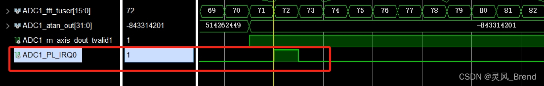
如上图,框起来的就是中断信号,它检测到valid信号的上升沿后,拉高一个高电平。
并且可以看出,此时写入BRAM的数据 ADC1_atan_out 为 -843314201
PS串口打印信息
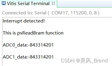
满足功能!


 507
507

 被折叠的 条评论
为什么被折叠?
被折叠的 条评论
为什么被折叠?
 到【灌水乐园】发言


