


 本文深入解析DDR存储技术的工作原理,包括存储单元结构、读写操作流程、时序控制及启动流程等关键内容,并探讨了DDR3新增的功能特性。
DDR存储原理
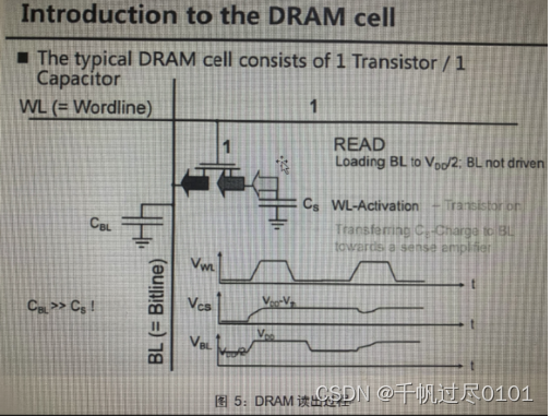
1. 1个三极管和1个电容构成一个最基本的存储单元。多个存储单元组合成存储矩阵,bit line连接到比较放大器,word line控制三极管的通断状态。相邻的、未使用的bit line上的电压作为参考电压,对比后经过放大输出0或1的状态。word line控制开关,bit line读写电容通道。64ms刷新,超温32ms
2. 写入过程:BL基准电压VDD/2,写1充电VDD,然后WL拉高打开三极管,对电容充电,然后WL拉低关闭三极管。写0放电到0,过程类似。
3. 读出过程:打开三极管,电容改变BL的电压,由于BL寄生电容远大于存储电容,因此BL电压变化很小,使用Sense amplifier放大。同时,刷新存储电容。
DDR实现
1. 沟道结构。硅片上打沟道,然后电镀生成电容。难度大,可靠性高。紫光国芯。
2. 堆叠结构。直接多次电镀生成电容。难度小,可靠性稍差。镁光。
DDR互联
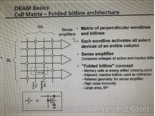
1. 阵列形式。行译码器,列译码器。
2. 行激活:WL打开一行三极管,读到BL并放大。列激活:将交叉点上的BL读入DQ,再经sense amplifier放大到VDD,再经Buffer输出到IO。
3. 相邻行的BL接在sense amplifier的2个输入端,互为参考。折叠式位线结构。开放式。
DDR时序
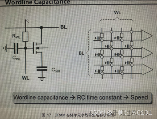
1. WL的寄生RC参数(Cwl和Rwl)影响运行速度和存储容量,对时序提出要求,不满足会丢数据。
2. tRCD:行激活时间。3步:WL打开三极管,电容对BL充当电,SA放大BL。
3. tCL:读命令时间。3步:BL到DQ,SA放大,Buffer驱动IO。
4. tWR:写入时间,写恢复
5. tRAS,tRP,tRC
DDR3新增功能
1. Reset引脚,关闭收发,关闭DLL,Clock
2. 写入延迟参数CWD
3. 突发长度固定8
4. 校准ZQ,240ohm,校准DQ输出导通电阻和ODT
5. 动态ODT,在线打开。
6. 参考电压分成2个,增加信噪等级
7. 点对点连接
8. 8预取,IO频率4倍core
DDR启动流程
1. 上电期间,上电后200us,输出IO和ODT必须保持高阻,RESET# 必须为LVCMOS低于 0.2VDDQ ,即0.7V。LVPECL输入低电平1.94V
2. RESET# 拉高之前10ns和拉高之后500us,CKE必须为低
3. 在CKE拉高前,CK必须稳定10ns或5个时钟周期,ODT至少为低Tis
CKE拉低后,想要拉高,只能使用NOP或DES
4. CKE拉高后,Txpr 以后,MRS命令加载MR2,MR3,MR1,MR0。
MR0,DLL锁定需要512个周期,Tdllk
5. ZQCL命令,校正RTT和RON,ZQinit。
6. Tdllk和ZQinit以后,启动完成,进入正常。
MR 2、3、1、0寄存器
7. DDR3突发长度4,8,读和写
突发顺序:顺序型,交错型
8. CAS latency
读指令,数据输出。2、3个周期
9. 复位DLL后,必须转回正常模式
10. 扩展MR。
使能关闭DLL,选择驱动强度。
AC/DC判别标准
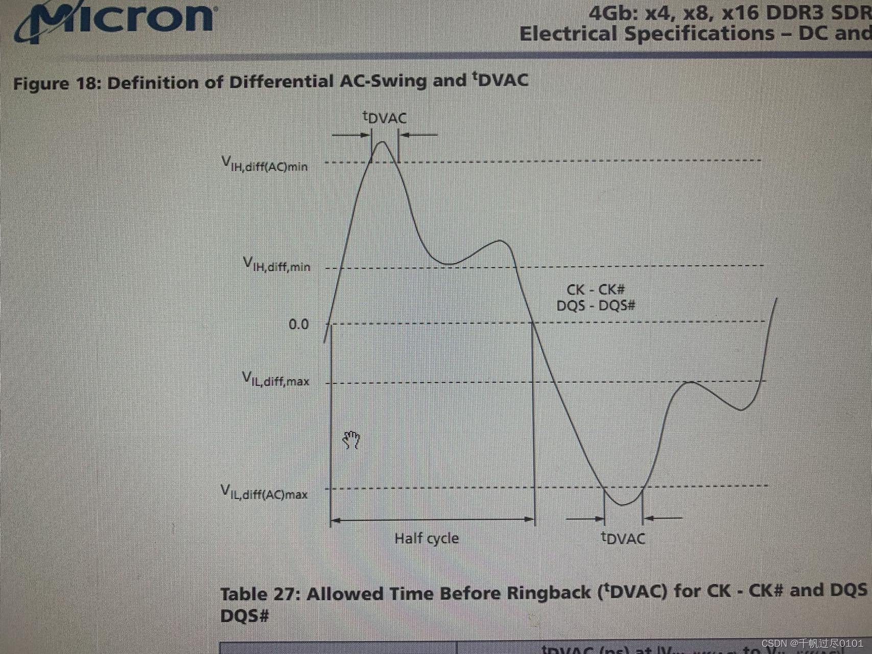
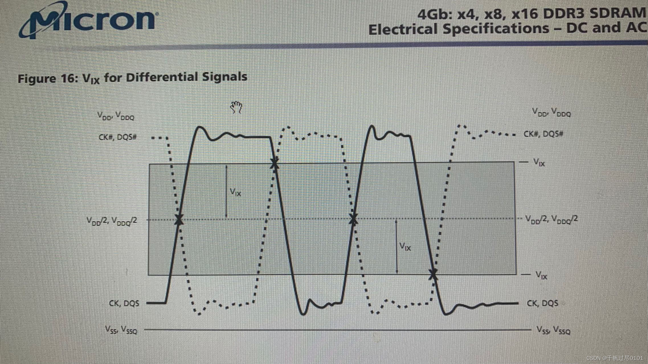
1. DQS和CK,差分信号电平要求
单端要求:Vseh和Vsel,Vref +/- 175mv
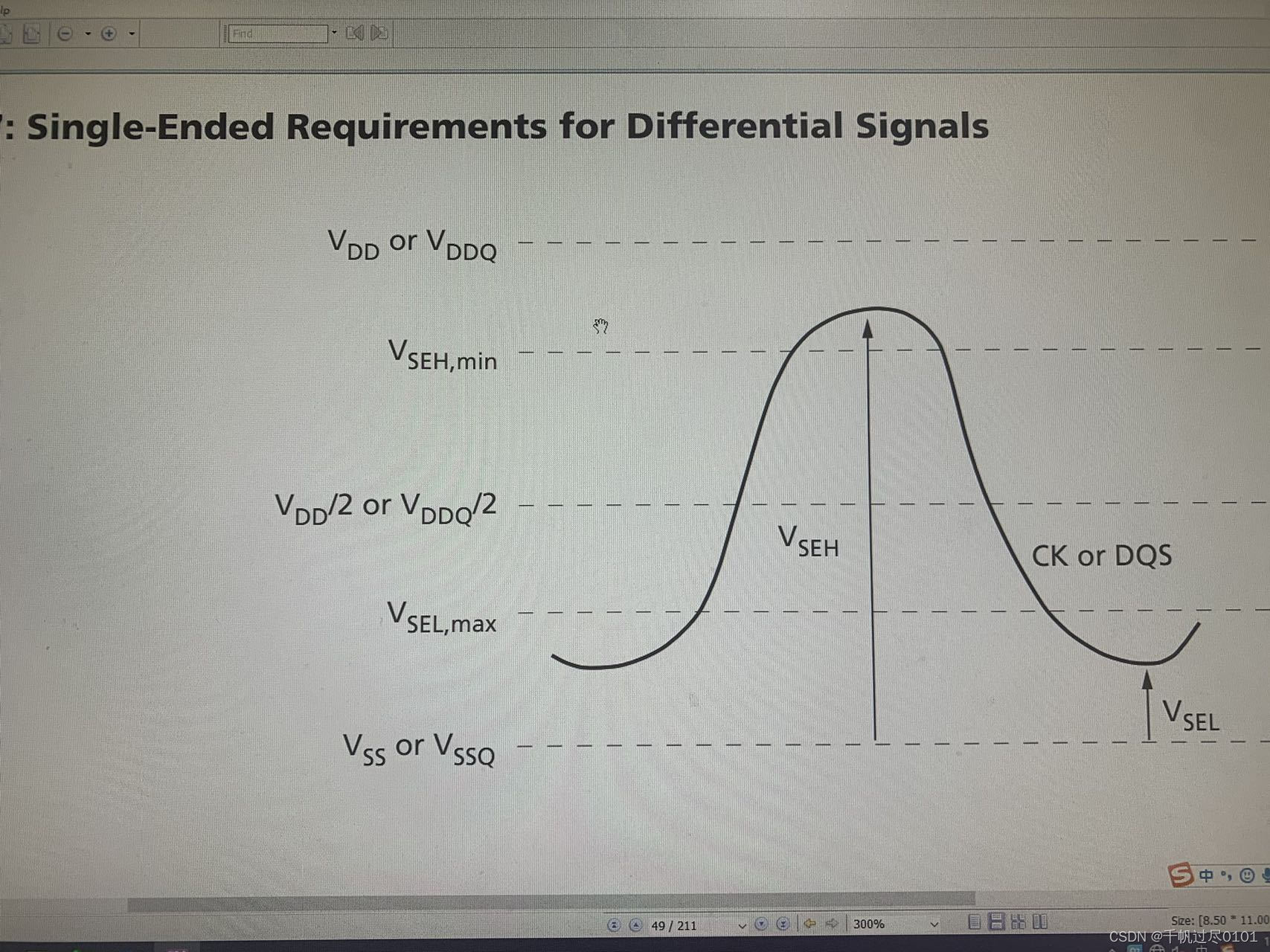
差分DC要求
Vihdiff,Vildiff:Vref +/- 200mv
差分AC要求
Vref +/- 2*135、150、175mv
2. DQS和CK,差分信号的交叉点要求,偏离参考电压不能大于150mv,即,Vix最大150mv
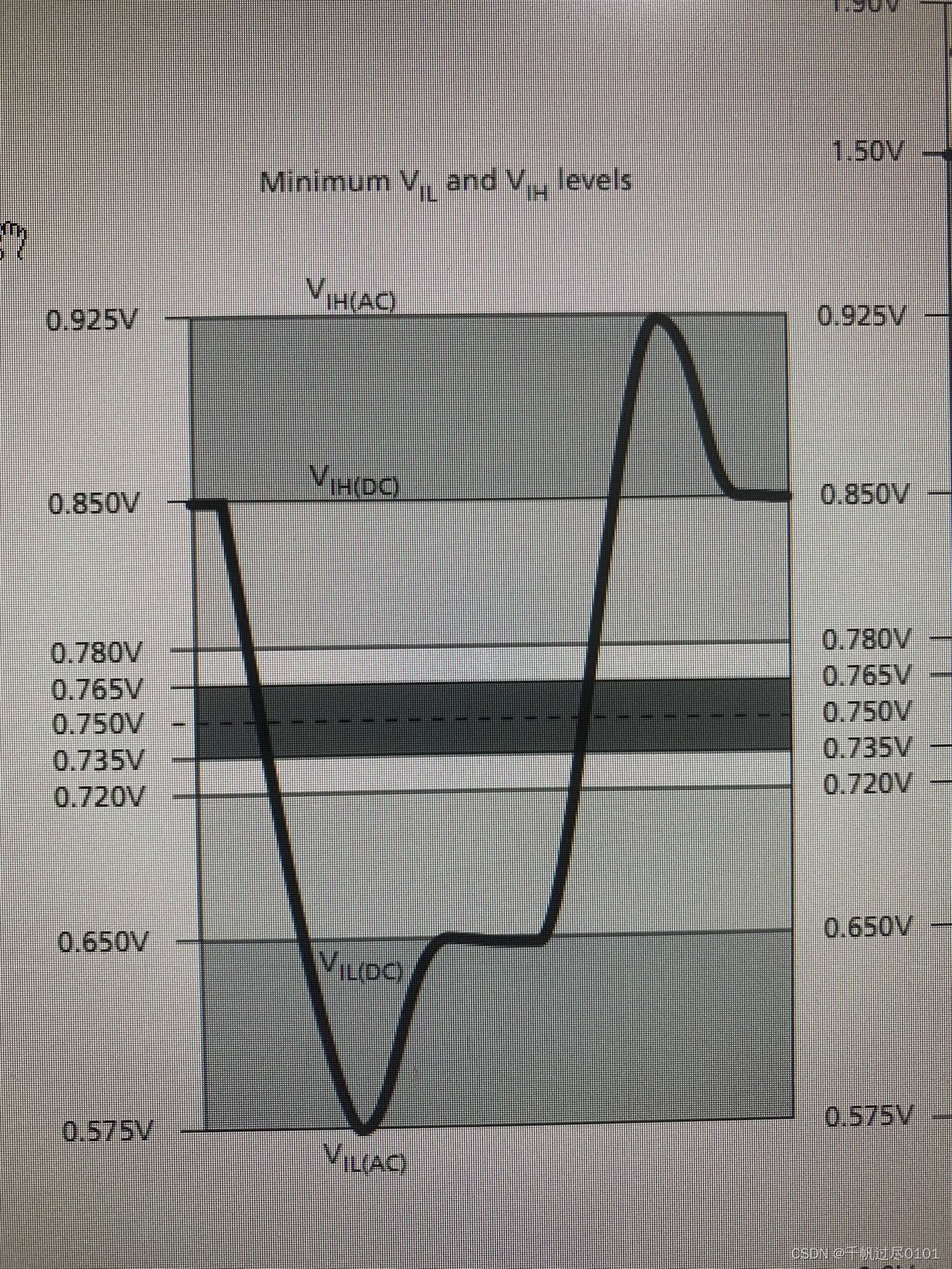
3. 单端信号DQ,DM,命令,地址,控制的电平要求
DC:100mv AC:135、150、175mv
4. CK采样控制和地址,DQS采样DQ和DM
5. DDR3区分参考信号。VrefDQ用于DQS,DM,DQ,追踪0.5VDD。VrefCA用于CK,地址,控制信号,追踪0.5VDD。精度要求为1%,即+/-15mv。


 1万+
1万+

 被折叠的 条评论
为什么被折叠?
被折叠的 条评论
为什么被折叠?
 到【灌水乐园】发言


