


FPGA HDL源程序
FPGA统计摄像头的输出像素,窗口尺寸等等
//----------------------------------------------------------------------------
// user_logic.v - module
//----------------------------------------------------------------------------
//
// ***************************************************************************
// ** Copyright (c) 1995-2012 Xilinx, Inc.  All rights reserved.            **
// **                                                                       **
// ** Xilinx, Inc.                                                          **
// ** XILINX IS PROVIDING THIS DESIGN, CODE, OR INFORMATION "AS IS"         **
// ** AS A COURTESY TO YOU, SOLELY FOR USE IN DEVELOPING PROGRAMS AND       **
// ** SOLUTIONS FOR XILINX DEVICES.  BY PROVIDING THIS DESIGN, CODE,        **
// ** OR INFORMATION AS ONE POSSIBLE IMPLEMENTATION OF THIS FEATURE,        **
// ** APPLICATION OR STANDARD, XILINX IS MAKING NO REPRESENTATION           **
// ** THAT THIS IMPLEMENTATION IS FREE FROM ANY CLAIMS OF INFRINGEMENT,     **
// ** AND YOU ARE RESPONSIBLE FOR OBTAINING ANY RIGHTS YOU MAY REQUIRE      **
// ** FOR YOUR IMPLEMENTATION.  XILINX EXPRESSLY DISCLAIMS ANY              **
// ** WARRANTY WHATSOEVER WITH RESPECT TO THE ADEQUACY OF THE               **
// ** IMPLEMENTATION, INCLUDING BUT NOT LIMITED TO ANY WARRANTIES OR        **
// ** REPRESENTATIONS THAT THIS IMPLEMENTATION IS FREE FROM CLAIMS OF       **
// ** INFRINGEMENT, IMPLIED WARRANTIES OF MERCHANTABILITY AND FITNESS       **
// ** FOR A PARTICULAR PURPOSE.                                             **
// **                                                                       **
// ***************************************************************************
//
//----------------------------------------------------------------------------
// Filename:          user_logic.v
// Version:           1.00.a
// Description:       User logic module.
// Date:              Fri Jun 13 15:26:29 2014 (by Create and Import Peripheral Wizard)
// Verilog Standard:  Verilog-2001
//----------------------------------------------------------------------------
// Naming Conventions:
//   active low signals:                    "*_n"
//   clock signals:                         "clk", "clk_div#", "clk_#x"
//   reset signals:                         "rst", "rst_n"
//   generics:                              "C_*"
//   user defined types:                    "*_TYPE"
//   state machine next state:              "*_ns"
//   state machine current state:           "*_cs"
//   combinatorial signals:                 "*_com"
//   pipelined or register delay signals:   "*_d#"
//   counter signals:                       "*cnt*"
//   clock enable signals:                  "*_ce"
//   internal version of output port:       "*_i"
//   device pins:                           "*_pin"
//   ports:                                 "- Names begin with Uppercase"
//   processes:                             "*_PROCESS"
//   component instantiations:              "<ENTITY_>I_<#|FUNC>"
//----------------------------------------------------------------------------

`uselib lib=unisims_ver
`uselib lib=proc_common_v3_00_a

module user_logic
(
  // -- ADD USER PORTS BELOW THIS LINE ---------------
  // --USER ports added here
  HREF_IN,
  VSYNC_IN,
  PCLK_IN,
  // -- ADD USER PORTS ABOVE THIS LINE ---------------

  // -- DO NOT EDIT BELOW THIS LINE ------------------
  // -- Bus protocol ports, do not add to or delete
  Bus2IP_Clk,                     // Bus to IP clock
  Bus2IP_Resetn,                  // Bus to IP reset
  Bus2IP_Data,                    // Bus to IP data bus
  Bus2IP_BE,                      // Bus to IP byte enables
  Bus2IP_RdCE,                    // Bus to IP read chip enable
  Bus2IP_WrCE,                    // Bus to IP write chip enable
  IP2Bus_Data,                    // IP to Bus data bus
  IP2Bus_RdAck,                   // IP to Bus read transfer acknowledgement
  IP2Bus_WrAck,                   // IP to Bus write transfer acknowledgement
  IP2Bus_Error                    // IP to Bus error response
  // -- DO NOT EDIT ABOVE THIS LINE ------------------
); // user_logic

// -- ADD USER PARAMETERS BELOW THIS LINE ------------
// --USER parameters added here
// -- ADD USER PARAMETERS ABOVE THIS LINE ------------

// -- DO NOT EDIT BELOW THIS LINE --------------------
// -- Bus protocol parameters, do not add to or delete
parameter C_NUM_REG                      = 4;
parameter C_SLV_DWIDTH                   = 32;
// -- DO NOT EDIT ABOVE THIS LINE --------------------

// -- ADD USER PORTS BELOW THIS LINE -----------------
// --USER ports added here
input VSYNC_IN;
input HREF_IN ;
input PCLK_IN ;
// -- ADD USER PORTS ABOVE THIS LINE -----------------

// -- DO NOT EDIT BELOW THIS LINE --------------------
// -- Bus protocol ports, do not add to or delete
input                                     Bus2IP_Clk;
input                                     Bus2IP_Resetn;
input      [C_SLV_DWIDTH-1 : 0]           Bus2IP_Data;
input      [C_SLV_DWIDTH/8-1 : 0]         Bus2IP_BE;
input      [C_NUM_REG-1 : 0]              Bus2IP_RdCE;
input      [C_NUM_REG-1 : 0]              Bus2IP_WrCE;
output     [C_SLV_DWIDTH-1 : 0]           IP2Bus_Data;
output                                    IP2Bus_RdAck;
output                                    IP2Bus_WrAck;
output                                    IP2Bus_Error;
// -- DO NOT EDIT ABOVE THIS LINE --------------------

//----------------------------------------------------------------------------
// Implementation
//----------------------------------------------------------------------------

  // --USER nets declarations added here, as needed for user logic

  // Nets for user logic slave model s/w accessible register example
  reg        [C_SLV_DWIDTH-1 : 0]           slv_reg0;
  reg        [C_SLV_DWIDTH-1 : 0]           slv_reg1;
  reg        [C_SLV_DWIDTH-1 : 0]           slv_reg2;
  reg        [C_SLV_DWIDTH-1 : 0]           slv_reg3;
  wire       [3 : 0]                        slv_reg_write_sel;
  wire       [3 : 0]                        slv_reg_read_sel;
  reg        [C_SLV_DWIDTH-1 : 0]           slv_ip2bus_data;
  wire                                      slv_read_ack;
  wire                                      slv_write_ack;
  integer                                   byte_index, bit_index;

  // USER logic implementation added here

  // ------------------------------------------------------
  // Example code to read/write user logic slave model s/w accessible registers
  //
  // Note:
  // The example code presented here is to show you one way of reading/writing
  // software accessible registers implemented in the user logic slave model.
  // Each bit of the Bus2IP_WrCE/Bus2IP_RdCE signals is configured to correspond
  // to one software accessible register by the top level template. For example,
  // if you have four 32 bit software accessible registers in the user logic,
  // you are basically operating on the following memory mapped registers:
  //
  //    Bus2IP_WrCE/Bus2IP_RdCE   Memory Mapped Register
  //                     "1000"   C_BASEADDR + 0x0
  //                     "0100"   C_BASEADDR + 0x4
  //                     "0010"   C_BASEADDR + 0x8
  //                     "0001"   C_BASEADDR + 0xC
  //
  // ------------------------------------------------------

  assign
    slv_reg_write_sel = Bus2IP_WrCE[3:0],
    slv_reg_read_sel  = Bus2IP_RdCE[3:0],
    slv_write_ack     = Bus2IP_WrCE[0] || Bus2IP_WrCE[1] || Bus2IP_WrCE[2] || Bus2IP_WrCE[3],
    slv_read_ack      = Bus2IP_RdCE[0] || Bus2IP_RdCE[1] || Bus2IP_RdCE[2] || Bus2IP_RdCE[3];

  // implement slave model register(s)
  always @( posedge Bus2IP_Clk )
    begin

      if ( Bus2IP_Resetn == 1'b0 )
        begin
          slv_reg0 <= 0;
          slv_reg1 <= 0;
          slv_reg2 <= 0;
          slv_reg3 <= 0;
        end
      else
        case ( slv_reg_write_sel )
          4'b1000 :
            for ( byte_index = 0; byte_index <= (C_SLV_DWIDTH/8)-1; byte_index = byte_index+1 )
              if ( Bus2IP_BE[byte_index] == 1 )
                slv_reg0[(byte_index*8) +: 8] <= Bus2IP_Data[(byte_index*8) +: 8];
          4'b0100 :
            for ( byte_index = 0; byte_index <= (C_SLV_DWIDTH/8)-1; byte_index = byte_index+1 )
              if ( Bus2IP_BE[byte_index] == 1 )
                slv_reg1[(byte_index*8) +: 8] <= Bus2IP_Data[(byte_index*8) +: 8];
          4'b0010 :
            for ( byte_index = 0; byte_index <= (C_SLV_DWIDTH/8)-1; byte_index = byte_index+1 )
              if ( Bus2IP_BE[byte_index] == 1 )
                slv_reg2[(byte_index*8) +: 8] <= Bus2IP_Data[(byte_index*8) +: 8];
          4'b0001 :
            for ( byte_index = 0; byte_index <= (C_SLV_DWIDTH/8)-1; byte_index = byte_index+1 )
              if ( Bus2IP_BE[byte_index] == 1 )
                slv_reg3[(byte_index*8) +: 8] <= Bus2IP_Data[(byte_index*8) +: 8];
          default : begin
            slv_reg0 <= slv_reg0;
            slv_reg1 <= slv_reg1;
            slv_reg2 <= slv_reg2;
            slv_reg3 <= slv_reg3;
                    end
        endcase

    end // SLAVE_REG_WRITE_PROC


  // ------------------------------------------------------------
  // Example code to drive IP to Bus signals
  // ------------------------------------------------------------

  assign IP2Bus_Data = (slv_read_ack == 1'b1) ? slv_ip2bus_data :  0 ;
  assign IP2Bus_WrAck = slv_write_ack;
  assign IP2Bus_RdAck = slv_read_ack;
  assign IP2Bus_Error = 0;

wire rst 	;
assign rst = slv_reg0[0];

reg[3:0] frame_end = 0;
reg[31:0] frame_count = 0;  //2 times of frame

always @(posedge VSYNC_IN or negedge rst)
begin
	if(1'b0 == rst)
	begin
		frame_count <= 32'h0;
		frame_end   <= 4'b0 ;
	end
	else
	begin
		frame_count <= frame_count + 1'b1;
		frame_end   <= frame_end   + 1'b1;
	end
end

reg[15:0] colum_count = 0;
reg[11:0] colum_end  = 0;
wire [15:0] colum_count_wire;
assign colum_count_wire = ((4'hf != frame_end)&&(4'h1 != frame_end)) ? colum_count : 16'h0;

always @(posedge HREF_IN or negedge rst )
begin
	if(1'b0 == rst)
	begin
		colum_end	<= 12'h0;
		colum_count <= 16'h0;
	end
	else
	begin
		if((1'b1 == VSYNC_IN)&&(4'h1 == frame_end))
		begin
			colum_count <= colum_count + 1'b1;
			colum_end   <= colum_end + 1'b1;
		end
		else if (4'hf == frame_end)
		begin
			colum_count <= 16'h0;
			colum_end   <= colum_end + 1'b1;
		end
		else
		begin
			colum_count <= colum_count;
			colum_end   <= colum_end + 1'b1;
		end
	end
end

reg[15:0] row_count = 0;
wire[15:0] row_count_wire;
assign row_count_wire = ((12'hfff != colum_end)&&(12'h02 != colum_end)) ? row_count : 16'h0;

always @(posedge PCLK_IN or negedge rst )
begin
	if (1'b0 == rst)
	begin
		row_count  <= 16'h0;
	end
	else
	begin
		if((1'b1 == HREF_IN)&&(12'h02 == colum_end))
		begin
			row_count <= row_count + 1'b1;
		end
		else if (12'hfff == colum_end)
		begin
			row_count <= 16'h00;
		end
		else
		begin
			row_count <= row_count;
		end
	end
end

//statiscal the time of a frame
reg[31:0] pixel_count = 0;
wire [31:0] pixel_count_wire;
assign pixel_count_wire =  ((4'h1  != frame_end)&&(4'hf != frame_end)) ? pixel_count : 31'h0;

always @(posedge Bus2IP_Clk or negedge rst)
begin
	if (1'b0 == rst)
	begin
		pixel_count <= 32'h0;
	end
	else
	begin
		if(4'h1 == frame_end)
		begin
			pixel_count <= pixel_count + 1'b1 ;
		end
		else if (4'hf == frame_end)
		begin
			pixel_count <= 31'h0;
		end
		else
		begin
			pixel_count <= pixel_count;
		end
	end
end

wire[31:0] row_colum_count;
assign row_colum_count ={ colum_count_wire ,row_count_wire};
  // implement slave model register read mux
  always @( slv_reg_read_sel or slv_reg0 or slv_reg1 or slv_reg2 or slv_reg3 )
    begin

      case ( slv_reg_read_sel )
        4'b1000 : slv_ip2bus_data <= slv_reg0;
        4'b0100 : slv_ip2bus_data <= row_colum_count;
        4'b0010 : slv_ip2bus_data <= frame_count;
        4'b0001 : slv_ip2bus_data <= pixel_count_wire;
        default : slv_ip2bus_data <= 0;
      endcase

    end // SLAVE_REG_READ_PROC


endmodule
SDK源程序
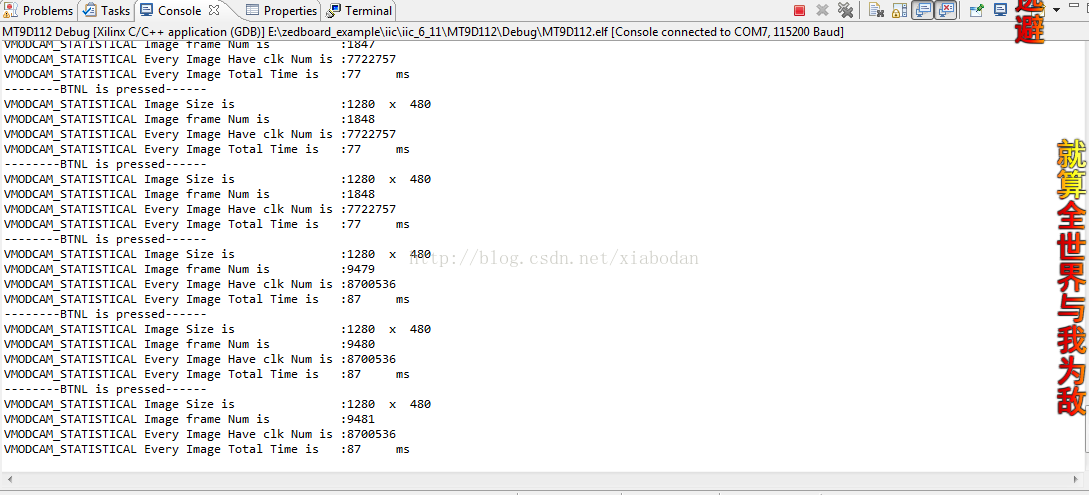
  printf("**********VmodCAM Image Statis Reret******\n");
  VMODCAM_STATISTICAL_mWriteSlaveReg0(XPAR_VMODCAM_STATISTICAL_0_BASEADDR,0,0);
  DelayMs(50);
  VMODCAM_STATISTICAL_mWriteSlaveReg0(XPAR_VMODCAM_STATISTICAL_0_BASEADDR,0,1);
  printf("********************end*******************\n");
if(BTNL == Status)
{
Status = VMODCAM_STATISTICAL_mReadSlaveReg1(XPAR_VMODCAM_STATISTICAL_0_BASEADDR,0);
printf("VMODCAM_STATISTICAL Image Size is :%d x %d\n",Status&0xffff,Status>>16);
Status = VMODCAM_STATISTICAL_mReadSlaveReg2(XPAR_VMODCAM_STATISTICAL_0_BASEADDR,0);
printf("VMODCAM_STATISTICAL Image Frame Num is :%d \n",Status);
Status = VMODCAM_STATISTICAL_mReadSlaveReg3(XPAR_VMODCAM_STATISTICAL_0_BASEADDR,0);
printf("VMODCAM_STATISTICAL Every Image Have clk Num is :%d \n",Status);
printf("VMODCAM_STATISTICAL Every Image Total Time is :%d ms \n",Status/100000);
}
输出RGB565分析
首先我们设置输出模式为RGB565: IIC设置【Rx2797】为0x0020
				0x33,0x8C,0x27,0x97, // Output format; Context B shadow
				0x33,0x90,0x00,0x20, // RGB with BT656 codes
0x33,0x8C,0x27,0x07, // Output width; Context B
0x33,0x90,0x02,0x80, // 640
0x33,0x8C,0x27,0x09, // Output height; Context B
0x33,0x90,0x01,0xe0, // 480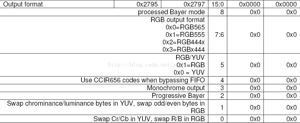
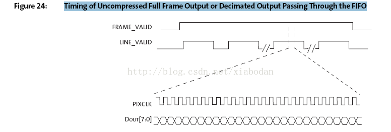
注: VMODCAM_STATISTICAL Image Size is :1280 x 480 其实就是标准的640 x 480 也就是480 行640 列 见下图
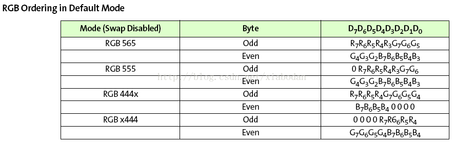
RGB565也就是一个像素占两个字节 奇字节分别是R7-R3 G7-G5
偶字节分别是G4-G3 B7-B3 其中G 占6个位
其他的类似。
参考:
datasheet 1/4-Inch 2Mp System-On-A-Chip (SOC) CMOS Digital Image Sensor
http://blog.csdn.net/xiabodan/article/details/30256297
实验室老师说的在空间里面只发布玩耍的心情,就代表没做事,没学习。我只想说为他们悲哀,真不知廉耻。还以为没人都想他们一样工作狂


 1599
1599

 被折叠的 条评论
为什么被折叠?
被折叠的 条评论
为什么被折叠?
 到【灌水乐园】发言


