


名称:MIPS多周期处理器Verilog代码Quartus仿真(文末获取)
软件:Quartus
语言:Verilog
代码功能:
MIPS多周期处理器
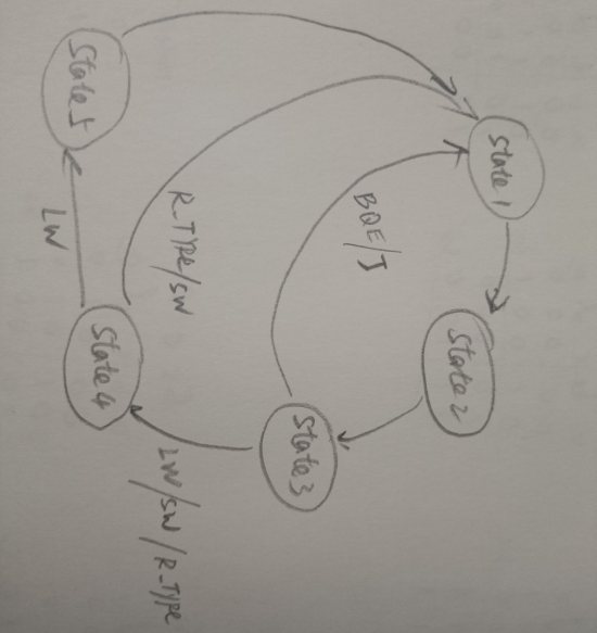
##### Operation a
Load the data stored in locations X of the data memory into registers P.
P register=reg 4,X=22
1. *load* operation is `100011`.
2. *base* is `00000`.
3. *rt* is `00100` because P register=reg 4.
4. *offset* is `10110`, because the X=22 .
| LW | base | rt | offset |
| :----: | :---: | :---: | :--------------: |
| 100011 | 00000 | 00100 | 0000000001011000 |
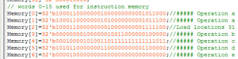
| 10001100000001000000000001011000 |
##### Operation a
Load the data stored in locations Y of the data memory into registers Q.
1. *load* operation is `100011`.
2. *base* is `00000`.
3. *rt* is `00101` because Q register=reg 5.
4. *offset* is `10111`, because the Y=23 .
| LW | base | rt | offset |
| :----: | :---: | :---: | :--------------: |
| 100011 | 00000 | 00101 | 0000000001011100 |
| 10001100000001010000000001011100 |
##### Operation a
Load the data stored in locations 31 of the data memory into registers 1.
1. *load* operation is `100011`.
2. *base* is `00000`.
3. *rt* is `00001` because register=reg 1.
4. *offset* is `11111`, because the 31 .
| LW | base | rt | offset |
| :----: | :---: | :---: | :--------------: |
| 100011 | 00000 | 00001 | 0000000001111100 |
| 10001100000000010000000001111100 |
##### Operation b
Add register P with constant 6 and store the result in the register R
The reasons:
add operation is 00000.
rs is 00100 because the P register is 4.
rt is 00001 because the 1 register is 1.
rd is 00110 because the R register is 6.
ADDUrs rt rd
00000000100000010011000000100000
00000000100000010011000000100000
##### Operation c
If the result in registers Q and R is equal to each other,
then branch to instruction a
beq是一条条件转移指令:beq rs,rt, label # if (rs==rt) pc<---label
1. *BEQ* operation is `000100`.
2. *rs* is `00101` because the Q register is 5.
3. *rt* is `00110` because the R register is 6.
4. *label* is `11000` because the memory location is 24.
| BEQ | rs | rt | label |
| :----: | :---: | :---: | :--------------: |
| 000100 | 00101 | 00110 | 1111111111111011 |
| 00010000101001101111111111111011 |
##### Operation d
Store the result in the register R into the memory location 24
1. *store* operation is `101011`.
2. *base* is `00000`.
3. *rt* is `00110` because the R register is 6.
4. *offset* is `11000` because the memory location is 24.
| SW | base | rt | offset |
| :----: | :---: | :---: | :--------------: |
| 101011 | 00000 | 00110 | 0000000001100000 |
| 10101100000001100000000001100000 |
##### Operation e
Jump to instruction a
1. *jump* operation is `000010`.
| J | target address |
| :----: | :------------------------: |
| 000010 | 00000000000000000000000000 |
| 00001000000000000000000000000000 |
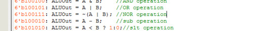
AND,func=100100
OR ,func=100101
sub,func=100010
slt,func=101010
NOR func=100111
100100: ALUOut <= A & B;
100101: ALUOut <= A | B;
100111: ALUOut <= ~(A | B);
100010: ALUOut <= A - B;
101010: ALUOut <= A < B ? 1:0;
##### Operation sub
**Q** sub **P** registers and store the result in the **R** register.
The reasons:
rs-rt=rd
1. *sub* R_Type is `000000`, func=100010.
2. *rs* is `00101` because the Q register is 5.
3. *rt* is `00100` because the P register is 4.
4. *rd* is `00110` because the R register is 6.
| SUB | rs | rt | rd | | func |
![]()
指令如下:

指令仿真图(Q=R后跳转到起始地址)
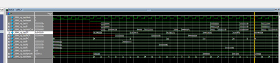
指令仿真图(Q/=R,存储R到mem[24],后跳转到起始地址)
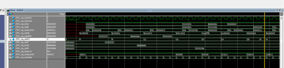


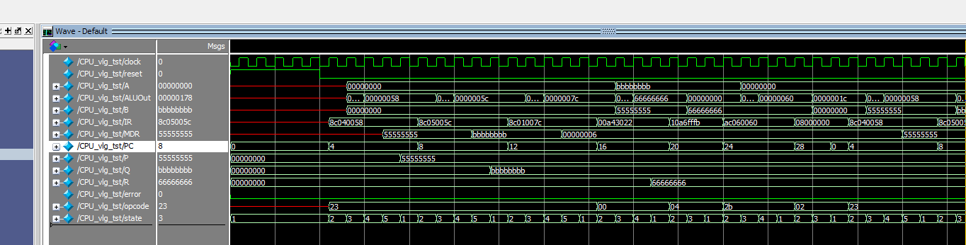
减法仿真(bbbbbbbb-55555555=66666666):

部分代码展示:
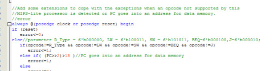
// The behavioural specification of a MIPS multicycle processor originaly developed
//for simulation by Patterson and Hennesy
// Modified by Dr. M. Xu in June 2010
module CPU (clock, reset, opcode, state, PC, IR, ALUOut, MDR, A, B, P, Q, R,error);
parameter R_Type = 6'b000000, LW = 6'b100011, SW = 6'b101011, BEQ=6'b000100,
J=6'b000010;
input clock, reset; //external inputs
output [31:0] PC, IR, ALUOut, MDR, A, B, P, Q, R;
output [2:0] state;
output [5:0] opcode;
output error;
// The architecturally visible registers and scratch registers for implementation
reg [31:0] PC, Regs[0:31], Memory [0:31], IR, ALUOut, MDR, A, B;
reg error;
reg [2:0] state; // processor state
wire [5:0] opcode; //use to get opcode easily
wire [31:0] SignExtend,PCOffset; //used to get sign extended offset field
assign opcode = IR[31:26]; //opcode is upper 6 bits
assign SignExtend = {{16{IR[15]}},IR[15:0]}; //sign extension of lower 16-bits of instruction
assign PCOffset = SignExtend << 2; //PC offset is shifted
assign P = Regs[4]; // you must change registers according to your tasks !
assign Q = Regs[5];
assign R = Regs[6];
// set the PC to 0 and start the control in state 1
initial begin PC = 0; state = 1; end
//The state machine--triggered on a rising clock
always @(posedge clock or posedge reset) begin
Regs[0] = 0; // to make sure R0 is always 0
if (reset) begin
PC = 0;
源代码
扫描文章末尾的公众号二维码


 613
613


 被折叠的 条评论
为什么被折叠?
被折叠的 条评论
为什么被折叠?
 到【灌水乐园】发言


