


Reference Design:Isolated 50 Watt Flyback Converter Using the UCC3809 Primary Side Controller
参考设计:使用 UCC3809 初级侧控制器的隔离式 50 瓦反激式转换器
APPLICATION NOTE U-165 - SLUU096 - JUNE 2001
Lisa Dinwoodie
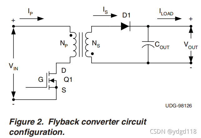
The basic flyback converter topology is shown in Figure 2.
基本的反激式转换器拓扑如图 2 所示。
The DC transfer function of a CCM flyback converter is:
CCM 反激式转换器的直流传递函数为:
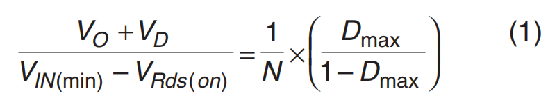
where VO equals the output voltage, 5V
其中 VO 等于输出电压,5V
VD = forward voltage drop across rectifier D1, assumed to be 0.8V
VD = 整流器 D1 上的正向压降,假设为 0.8V
VIN = 32 to 72V, VIN(min) = 32V
VIN = 32 至 72V,VIN(min) = 32V
VRds(on) = on voltage drop across MOSFET Q1,equal to Rds(on) x I(primary), assumed to be 1V
VRds(on) = MOSFET Q1 上的导通压降,等于 Rds(on) x I(primary),假设为 1V
N = turns ratio, equal to NP/NS
N = 匝数比,等于 NP/NS
NS = number of transformer secondary turns
NS = 变压器次级匝数
NP = number of transformer primary turns
NP = 变压器初级匝数
D = duty cycle
D = 占空比
Maximum duty cycle, 0.45, occurs at minimum input voltage. Substituting these values into (1) gives us a turns ratio of 4.66.
最大占空比 0.45 出现在最小输入电压下。 将这些值代入 (1) 得到 4.66 的匝数比。
The turns ratio is inversely proportional to the peak primary current, IPEAK, but directly proportional to the voltage stress on the switching element.
匝数比与峰值初级电流 IPEAK 成反比,但与开关元件上的电压应力成正比。
So the peak currents will not become unreasonably high and the voltage stress on the MOSFET will be kept as low as possible,the turns ratio is rounded up only to the next integer value, 5, or simply five primary turns for every one secondary turn.
因此,峰值电流不会变得不合理地高,并且 MOSFET 上的电压应力将保持尽可能低,匝数比仅四舍五入到下一个整数值 5,或者每一个次级匝数为 5 个初级匝数。
Recalculating equation (1) results in an actual Dmax of 48%.(非常重要!!!)
重新计算等式 (1) 导致实际 Dmax 为 48%。
1.Switching Frequency 开关频率
Because the magnetic components and filters will be smaller, the tendency is to have as high a switching frequency as possible.
因为磁性元件和滤波器会更小,所以倾向于具有尽可能高的开关频率。
Unfortunately, the decision is not quite that clear cut. Core losses,gate charge currents, and switching losses increase with higher switching frequencies; peak currents increase with lower switching frequencies.
不幸的是,这个决定并不是那么明确。 磁芯损耗、栅极充电电流和开关损耗随着开关频率的升高而增加; 峰值电流随着开关频率的降低而增加。
A compromise must be reached between component size, current levels, and acceptable losses. Synchronization with other systems and backward compatibility may also be deciding factors. For this design, a fixed frequency (fsw) of 70kHz was chosen. At Dmax equal to 48%, ton(max) becomes 6.9µs.
必须在元件尺寸、电流水平和可接受的损耗之间达成折衷。 与其他系统的同步和向后兼容性也可能是决定性因素。 对于此设计,选择了 70kHz 的固定频率 (fsw)。 在 Dmax 等于 48% 时,ton(max) 变为 6.9µs。
2.Transformer Design [2] 变压器设计
The transformer in a flyback converter is actually a coupled inductor with multiple windings. Transformers provide coupling and isolation whereasinductors provide energy storage. The energy stored in the air gap of the inductor is equal to:
反激式转换器中的变压器实际上是具有多个绕组的耦合电感器。 变压器提供耦合和隔离,而电感器提供能量存储。 存储在电感气隙中的能量等于:
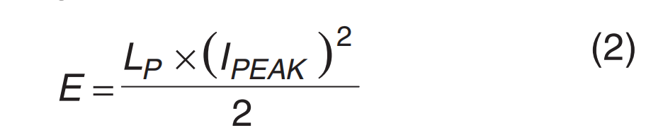
where E is in Joules, LP is the primary inductance in Henries, and IPEAK is the peak primary current in Amperes.
其中 E 以焦耳为单位,LP 是以亨利为单位的初级电感,IPEAK 是以安培为单位的峰值初级电流。
When the switch is on, D1 (from Figure 2) is reverse biased due to the dot configuration of the transformer. No current flows in the secondary windings and the current in the primary winding ramps up at a rate of:
当开关打开时,D1(来自图 2)由于变压器的同名端配置而反向偏置。 次级绕组中没有电流流动,初级绕组中的电流以以下速率上升:
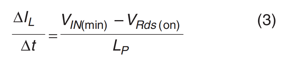 where VIN(min) and VRds(on) were defined previously and ∆t is equal to ton(max) at VIN(min). The output capacitor, COUT, supplies all of the load current at this time.
其中 VIN(min) 和 VRds(on) 先前已定义,Δt 等于 VIN(min) 处的 ton(max)。 此时,输出电容器 COUT 提供所有负载电流。
Because the converter is operating in the continuous conduction mode, ∆IL is the change in the inductor current which appears as a positive slope ramp on a step.
由于转换器在连续导通模式下运行,ΔIL 是电感电流的变化,它表现为阶跃的正斜率斜坡。
The step is present because there is still current left in the secondary windings when the primary turns on.
之所以存在阶跃,是因为在初级导通时次级绕组中仍有电流。
When the switch turns off, current flows through the secondary winding and D1 as a negative ramp on a step, replenishing COUT and supplying current directly to the load.
当开关关闭时,电流流过次级绕组和 D1 作为阶跃的负斜坡,补充 COUT 并直接向负载提供电流。
Based on (3), the primary inductance can be calculated given an acceptable current ripple, ΔIL.
根据 (3),初级电感可以计算出可接受的电流纹波 ΔIL。
For this design, ΔIL was set to equal one-half the peak primary current. For a CCM flyback design, the peak primary current is calculated based upon (4).
对于此设计,ΔIL 设置为等于峰值初级电流的二分之一。 对于 CCM 反激式设计,峰值初级电流是根据 (4) 计算的。
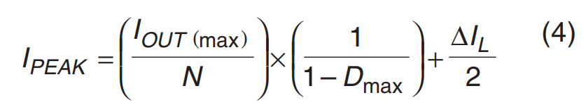
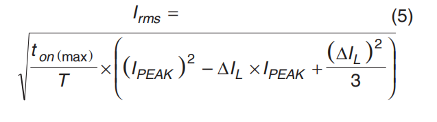
By replacing ΔIL with ½(IPEAK), IOUT(max) with 10A,Dmax with 0.48, and N with 5 as detailed earlier,the peak primary current is calculated to be 5.16A and ΔIL calculates to 2.58A. The root mean square,RMS, current of a ramp on a step waveform is defined in (5) and calculates to be 2.74A for this application.
通过将 ΔIL 替换为 ½(IPEAK),将 IOUT(max) 替换为 10A,将 Dmax 替换为 0.48,并将 N 替换为 5,如前面所述,峰值初级电流计算为 5.16A,ΔIL 计算为 2.58A。 阶跃波形上斜坡的均方根 RMS 电流在 (5) 中定义,并且对于此应用计算为 2.74A。
Using (3), LP calculates to approximately 80µH.
使用 (3),LP 计算为大约 80µH。
Due to cost considerations and a switching frequency of 70kHz, the core material was chosen to be manganese zinc ferrite 3C85 from Philips.
出于成本考虑和 70kHz 的开关频率,磁芯材料选择了飞利浦的锰锌铁氧体 3C85。
Because the inductor (a.k.a. the flyback transformer) is driven in one quadrant of the B-H plane only, a larger core is required in a flyback design.
由于电感器(又名反激变压器)仅在 B-H 平面的一个象限中驱动,因此反激设计需要更大的磁芯。
Because this converter is operating in the continuous conduction mode at a relatively low frequency, the maximum peak flux density, Bmax, is limited by the saturation flux density, Bsat.
由于该转换器以相对较低的频率在连续导通模式下运行,因此最大峰值磁通密度 Bmax 受饱和磁通密度 Bsat 的限制。
Taking all this into consideration, the minimum core size is determined by(6).
考虑到所有这些,最小磁芯尺寸由(6)确定。 (AP法)
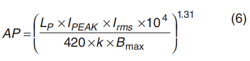
where AP = the core area product in cm4
其中 AP = 以 cm4 为单位的核心面积乘积
k = winding factor, equal to 0.2 for a continuous mode flyback
k = 绕组系数,对于连续模式反激式等于 0.2
Bmax ≈ Bsat, or 0.33 Telsa for 3C85 material at 100 ℃
Bmax ≈ Bsat,或 3C85 材料在 100 ℃ 时为 0.33 Telsa(特斯拉,3300高斯)
The result of (6) is compared to the product of the winding area, Aw (cm2), and effective core area,Ae (cm2), listed in the core manufacturer’s data sheet.
将 (6) 的结果与磁芯制造商数据表中列出的绕组面积 Aw (cm2) 和有效磁芯面积 Ae (cm2) 的乘积进行比较。
For this design, a Philips EFD30 core met the minimum criteria.
对于此设计,飞利浦 EFD30 内核满足最低标准。
The minimum number of primary turns is determined by:
初级匝数的最小值由以下因素决定:
Based upon this result and the predetermined turns ratio, the number of secondary turns is established. With a turns ratio of 5 and NP equal to 20, NS is calculated to be 4.
根据该结果和预定匝数比,确定次级匝数。 匝数比为 5 且 NP 等于 20 时,NS 计算为 4。
The energy stored in the flyback transformer is actually stored in an air gap in the core.This is because the high permeability of the ferrite material can’t store much energy without saturating first.
反激式变压器中储存的能量实际上储存在磁芯的气隙中。这是因为铁氧体材料的高磁导率,所以即便在达到饱和时也无法储存太多能量。
By adding an air gap, the hysteresis curve of the magnetic material is actually tilted, requiring a much higher field strength to saturate the core. The size of the air gap is calculated using (8).
通过增加气隙,磁性材料的磁滞曲线实际上是倾斜的,需要更高的场强来使磁芯饱和。 气隙的大小使用(8)计算。
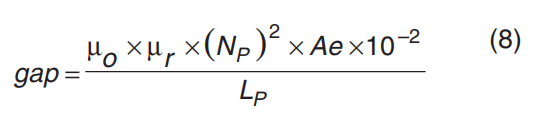
In (8), the gap is measured in centimeters, µo is the permeability of free space equal to 4 10-7 H/m, and µr is equal to the relative permeability of the gap material (in this case the gap material is air, µr=1).
在(8)中,间隙以厘米为单位,μo 是自由空间的磁导率,等于 4π*10^(-7) H/m,μr 等于间隙材料的相对磁导率(在这种情况下,间隙材料是空气 , µr=1)。
This gap is calculated to be 0.043cm and is evenly distributed between the center post and two outer legs of the EFD30 core.
该间隙经计算为 0.043 厘米,均匀分布在 EFD30 核心的中心柱和两个外腿之间。
The primary windings are two strands of 21AWG magnet wire in parallel, the first layer wound closest to the core, the second layer over the secondary windings. The secondary windings consist of four strands of 18AWG magnet wire in parallel, filling a single layer for maximum coupling.
初级绕组是两股平行的 21AWG 漆包线,第一层最靠近磁芯缠绕,第二层缠绕在次级绕组上。 次级绕组由四股平行的 18AWG 漆包线组成,填充单层以实现最大耦合。
Using a primary inductance of 80µH and a maximum duty cycle of 48% means the converter will not stay in continuous mode control over the entire operating range because of the relationship expressed in (9).
使用 80µH 的初级电感和 48% 的最大占空比意味着转换器不会在整个工作范围内保持连续模式控制,因为 (9) 中表达的关系。
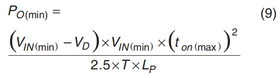
According to (9), at the 32V minimum input voltage the converter will enter discontinuous mode at an output load current of less than 3.33A. To remain in CCM would require a much larger transformer,264.5µH at 48% duty cycle. Increasing the primary inductor value requires a much larger core, such as the E41/17/2 core set from Philips. This would require 60% more circuit board space than the present core.
根据 (9),在 32V 最小输入电压下,转换器将在输出负载电流小于 3.33A 时进入不连续模式。 要保持在 CCM 中,需要更大的变压器,占空比为 48% 时为 264.5µH。 增加初级电感值需要更大的磁芯,例如飞利浦的 E41/17/2 磁芯组。 这将需要比现有核心多 60% 的电路板空间。
Another approach to guarantee remaining in continuous mode is to reduce the maximum duty cycle to approximately 26% and continue to use an 80µH flyback inductor.Unfortunately, the result of this would be considerably higher peak currents. Higher peak currents result in an increase of all the I2R losses, and a larger core would be needed anyway to satisfy the core area product limit which is dependent upon the peak primary current as expressed in (6).
另一种保证保持连续模式的方法是将最大占空比降低到大约 26% 并继续使用 80µH 反激电感。不幸的是,这样做的结果将是相当高的峰值电流。 更高的峰值电流会导致所有 I2R 损耗的增加,并且无论如何都需要更大的磁芯来满足磁芯面积乘积限制,该限制取决于 (6) 中表示的峰值初级电流。
It is far better to design for continuous mode and to transition into discontinuous mode than the other way around.
为连续模式设计并过渡到不连续模式比其他方式要好得多。
Discontinuous mode is actually unavoidable at zero load.
在零负载下,不连续模式实际上是不可避免的。
A continuous mode feedback control loop has the ability to maintain stability while in discontinuous mode.
连续模式反馈控制回路能够在不连续模式下保持稳定性。
However, a control loop designed for discontinuous operation does not take into account the already eluded to right-half-plane zero present in continuous mode.
然而,为不连续操作设计的控制回路没有考虑在连续模式中已经存在的右半平面零。
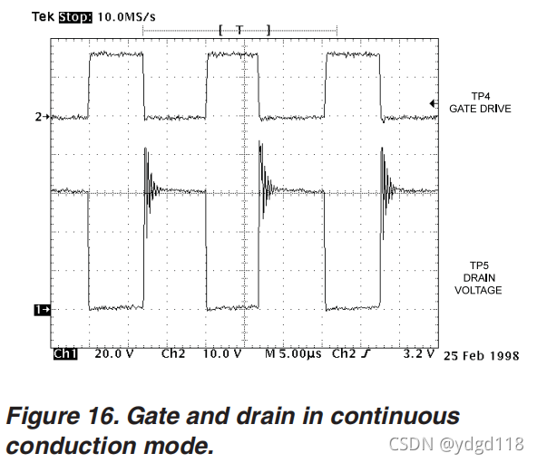
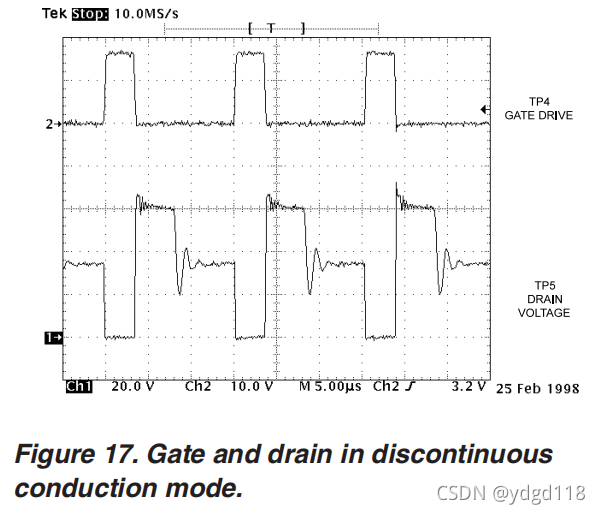
This design has the fortuitous advantage of showing the user waveforms for both operating modes dependent upon input voltage and load current (see Figures 16 and 17).
这种设计具有一个偶然的优势,即根据输入电压和负载电流显示两种工作模式的用户波形(见图 16 和 17)。
3.MOSFET Selection MOSFET选型
The switching element in a flyback converter must have a voltage rating high enough to handle the maximum input voltage and the reflected secondary voltage, not to mention any leakage inductance induced spike that is inevitably present. Approximate the required voltage rating of the MOSFET using (10).
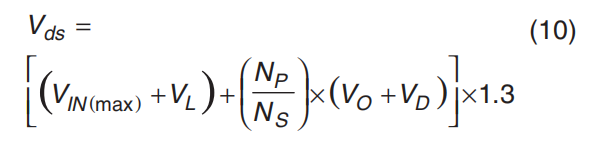
where Vds = the required drain to source voltage rating of the MOSFET
其中 Vds = MOSFET 所需的漏源电压额定值
VL = the voltage spike due to the leakage inductance of the transformer, estimated to be thirty percent of VIN(max)
VL = 由于变压器漏感引起的电压尖峰,估计为 VIN(max) 的百分之三十
and the additional 1.3 factor includes an overall thirty percent margin.
额外的 1.3 系数包括 30% 的余量。
For the flyback converter presented, the required minimum voltage rating of the MOSFET calculates to be 160V. An IRF640 N-channel power MOSFET was chosen.
对于所提供的反激式转换器,MOSFET 所需的最小额定电压计算为 160V。 选择了 IRF640 N 沟道功率 MOSFET。
This device has a voltage rating of 200V, a continuous DC current rating of 18A, and an Rds(on) of only 0.18Ω.
该器件的额定电压为 200V,连续额定直流电流为 18A,Rds(on) 仅为 0.18Ω。
By consulting the typical gate charge vs. gate-to-source voltage waveform in the anufacturer’s data book, calculating the average current required to drive the gate capacitor of the FET is possible:
通过查阅制造商数据手册中的典型栅极电荷与栅极-源极电压波形,可以计算驱动 FET 栅极电容器所需的平均电流:
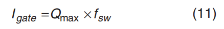
Qmax is the total gate charge in Coulombs, estimated to be 70nC based upon a gate to source voltage of 15V and a drain to source voltage of 160V.
Qmax 是以库仑为单位的总栅极电荷,根据 15V 的栅极至源极电压和 160V 的漏极至源极电压估计为 70nC。
According to (11), the average supply current of the controller, IVDD, needs to increase by 4.9mA to switch the gate at the selected operating frequency.
根据 (11),控制器的平均电源电流 IVDD 需要增加 4.9mA 才能在选定的工作频率下切换栅极。
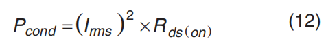
This FET will experience both switching and conduction losses. The conduction losses will be equal to the I2R losses, as shown by (12)
该 FET 将经历开关损耗和传导损耗。 传导损耗将等于 I2R 损耗,如 (12) 所示
Switching losses are the result of overlapping drain current and drain to source voltage at turn on and turn off [3].
At turn on the drain current begins to flow through the FET device when the gate voltage has reached the Vgs threshold. This drain current will continue to rise until reaching its final value.Meanwhile, the drain to source voltage will remain at Vds, calculated earlier in (10).
This voltage starts to fall only after the “Miller” capacitor begins to charge. The charging time, tch, for the “Miller” capacitor is a function of the gate resistor, Rg (R10 in Figure 1), and the gate to drain “Miller” charge,Qgd, as shown in (13).
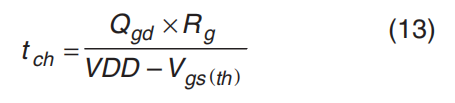
In (13), VDD is the bias voltage of the UCC3809 and Vgs(th) is the gate threshold voltage of the FET.
在 (13) 中,VDD 是 UCC3809 的偏置电压,Vgs(th) 是 FET 的栅极阈值电压。
The whole process repeats itself in reverse at turn off. The power dissipation of the FET’s output capacitance, Coss, also contributes to the switching losses in the form of ½C*V^2 f.
整个过程在关闭时反向重复。 FET 输出电容 Coss 的功耗也会以 ½CV^2 *f 的形式影响开关损耗。
The total switching losses are estimated based on equation (14).
总开关损耗是根据等式 (14) 估算的。
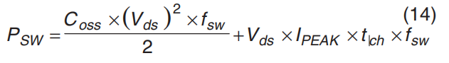
The total FET losses are the sum of the conduction losses (12) and the switching losses (14), calculated to be 3.3W for the IRF640 FET.
总 FET 损耗是传导损耗 (12) 和开关损耗 (14) 的总和,计算得出 IRF640 FET 为 3.3W。
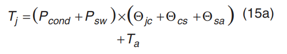
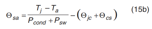
Without appropriate heatsinking, this device would have a junction to ambient thermal resistance of 62 ℃/W,resulting in a junction temperature rise of 206℃ above ambient.
如果没有适当的散热片,该器件将具有 62 ℃/W 的结到环境热阻,导致结温高于环境温度 206℃。
Heat sinking is obviously required to prevent the junction temperature, Tj, from exceeding 150 ℃and avert device failure due to excessive heating.
显然需要散热以防止结温 Tj 超过 150 ℃ 并避免由于过热而导致器件故障。
The IRF640 has a junction to case thermal resistance, θjc, of 1℃/W, using a silicone elastomer heat sink pad provides a case to heat sink thermal resistance, θcs , of 1.26℃/W.
IRF640 的结到外壳热阻 θjc 为 1℃/W,使用有机硅弹性体散热器垫提供外壳到散热器热阻 θcs 为 1.26℃/W。
A heat sink which provides a maximum thermal resis tance, sa, of 35 ℃/W must be chosen for a use in an ambient temperature, Ta, of 25 ℃, as shown in (15a) and (15b).
如 (15a) 和 (15b) 所示,必须选择最大热阻 sa 为 35 ℃/W 的散热器才能在 25 ℃ 的环境温度 Ta 中使用。
4.Diode Selection 二极管选型
Schottky rectifiers have a lower forward voltage drop than typical PN devices, making it the rectifier of choice when considering reducing converter losses and improving overall efficiency.
肖特基整流器的正向压降低于典型的 PN 器件,使其成为考虑降低转换器损耗和提高整体效率时的首选整流器。
Selecting the appropriate Schottky for a specific application depends mainly on the working peak reverse voltage rating, the peak repetitive forward current, and the average forward current rating of the device. If the maximum working peak reverse voltage is exceeded the reverse leakage current will rise above its specified limit.
为特定应用选择合适的肖特基主要取决于器件的工作峰值反向电压额定值、峰值重复正向电流和平均正向电流额定值。如果超过最大工作峰值反向电压,反向漏电流将上升到其规定的极限以上。
The peak reverse voltage that the device will be subjected to is equal to the reflected maximum input voltage minus the voltage drop across the FET added to the output voltage. The maximum average forward current rating of the device must not be exceeded if the junction temperature of the device is to remain within its safe operating range.
器件将承受的峰值反向电压等于反射的最大输入电压减去加到输出电压的 FET 两端的压降。如果器件的结温要保持在其安全工作范围内,则不得超过器件的最大平均正向电流额定值。
Because all current to the output capacitor and load must flow through the diode, the average forward diode current is equal to the steady-state load current. The peak repetitive forward current is equal to the reflected primary peak current.
因为所有流向输出电容器和负载的电流都必须流经二极管,所以二极管的平均正向电流等于稳态负载电流。峰值重复正向电流等于反射初级峰值电流。
An MBR2535CTL Schottky rectifier from Motorola met the requirements for the given design. This device is a common cathode dual Schottky with a forward voltage drop of 0.47V and a working peak reverse voltage rating of 35V, exceeding the 20V requirement of the design. The average rectified forward current rating is specified at 12.5A per leg, 25A total, and the peak repetitive forward current is rated for 25A per leg, or a total of 50A. The design requirement is 10A total average forward current and 26A total peak repetitive forward current.
摩托罗拉的 MBR2535CTL 肖特基整流器满足给定设计的要求。该器件为共阴极双肖特基,正向压降为 0.47V,工作峰值反向电压额定值为 35V,超过了设计的 20V 要求。平均整流正向电流额定值为每条腿 12.5A,总计 25A,峰值重复正向电流额定为每条腿 25A,或总计 50A。设计要求是 10A 总平均正向电流和 26A 总峰值重复正向电流。
Power loss in the Schotty is the summation of conduction losses and the reverse leakage losses.Conduction losses are calculated using the forward voltage drop and the average forward current.
Schotty 中的功率损耗是传导损耗和反向泄漏损耗的总和。传导损耗是使用正向压降和平均正向电流计算的。
The MBR2535CTL will have conduction losses equal to 4.7W. Reverse leakage losses, which are dependent upon the reverse leakage current, the blocking voltage, and the on-time of the FET, are alculated to be 0.05W.
MBR2535CTL 的传导损耗等于 4.7W。反向泄漏损耗取决于反向泄漏电流、阻断电压和 FET 的导通时间,计算结果为 0.05W。
Heat sink selection is once again based upon the required thermal resistance of the heat sink to air interface in order to maintain a junction temperture of less than 125 C.
散热器的选择再次基于散热器与空气界面所需的热阻,以保持结温低于 125°C。
5.input and Output Capacitors 输入输出电容器
The input capacitors are chosen based upon their ripple current rating and their rated voltage.
输入电容器的选择基于其纹波电流额定值和额定电压。
The input current waveform is shown in Figure 3. The shaded regions represent the current actually supplied by the input capacitors during the switch’s on and off-times.
输入电流波形如图 3 所示。阴影区域表示在开关导通和关断期间输入电容器实际提供的电流。
Because this example uses a duty cycle that is very close to 50%, this RMS current is almost equal to the primary RMS current calculated in (5).
由于此示例使用非常接近 50% 的占空比,因此此 RMS 电流几乎等于 (5) 中计算的初级 RMS 电流。
The actual capacitor value is not that critical as long as the minimum capacitance gives an acceptable ripple voltage determined by the following equation:
只要最小电容给出一个可接受的纹波电压,实际的电容值就不是那么重要了,该电压由下式确定:
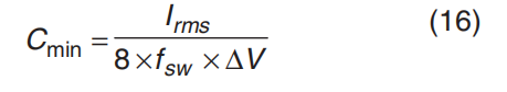
In (16), Irms is equal to the RMS current, calculated from Figure 3, and ΔV is equal to the acceptable ripple voltage.
在 (16) 中,Irms 等于根据图 3 计算的 RMS 电流,而 ΔV 等于可接受的纹波电压。
Two United Chemi-Con SXE series 150µF capacitors in parallel met the requirements for the design when derated for ambient temperature and frequency.
两个 United Chemi-Con SXE 系列 150µF 电容器并联后,在环境温度和频率降额时满足设计要求。
The small 1µF ceramic capacitor is added at the converter input to provide a shorter path for high frequency ripple.
在转换器**输入端添加了一个 **1μF 的小陶瓷电容器,以便为高频纹波提供更短的路径。
The output capacitors are also chosen based upon their low equivalent series resistance (ESR), ripple current and voltage ratings,and (16).
输出电容器的选择也基于它们的低等效串联电阻 (ESR)、纹波电流和电压额定值,以及 (16)。
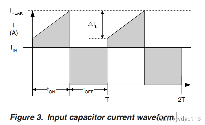
The ripple current that the output capacitor experiences is a result of supplying the load current during the FET conduction time and its charging current during the FET off-time, as illustrated by the shaded regions in Figure 4.
输出电容器经历的纹波电流是 FET 导通期间提供负载电流和 FET 关断期间提供充电电流的结果,如图 4 中的阴影区域所示。
During the conduction time of the FET,the secondary windings of the transformer are not conducting. The discharging of the output capacitor supplies the 10A load current.
在场效应管导通期间,变压器的次级绕组不导通。 输出电容器的放电提供 10A 负载电流。
During the FET off-time, the secondary windings are conducting and the secondary peak current is charging the output capacitor and delivering the 10A current to the load.
在 FET 关断期间,次级绕组导通,次级峰值电流为输出电容器充电并向负载提供 10A 电流。
The RMS current is calculated to be approximately 14A. Four Sanyo OSCON 6SH330M 330µF capacitors in parallel met the requirements for the demo board design when derated for ambient temperature and frequency.
计算得出的 RMS 电流约为 14A。 四个并联的 Sanyo OSCON 6SH330M 330µF 电容器在环境温度和频率降额时满足演示板设计的要求。
6.SNUBBERS AND CLAMPS [7]缓冲器和夹钳 [7]
Transformer leakage inductance imposes high transients in the switch, requiring a switching device with an excessive voltage rating.
变压器漏感会在开关中产生高瞬态,需要具有过高额定电压的开关器件。
The primary side of the demo board utilizes a passive polarized voltage clamp (Figure 12) to suppress the voltage overshoot during the turn-off transition of the FET.
演示板的初级侧利用无源极化电压钳位(图 12)来抑制 FET 关断转换期间的电压过冲。
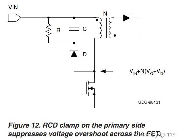 This circuit limits the peak switch voltage, reducing the power dissipation in the switching device. The total dissipated energy remains the same, but it is now divided between the clamp resistor and the FET.
该电路限制了峰值开关电压,从而降低了开关器件的功耗。 总耗散能量保持不变,但现在在钳位电阻器和 FET 之间分配。
The parasitic inductance of the transformer is discharged into the capacitor during each switching cycle.
变压器的寄生电感在每个开关周期内放电到电容器中。
The value of the capacitor is selected based upon the amount of energy that this leakage inductance stores plus the initial energy stored in the capacitor from the input voltage and the reflected output voltage.
根据该漏电感存储的能量加上电容器中存储的来自输入电压和反射输出电压的初始能量来选择电容器的值。
Equation 32 determines the minimum capacitor value.
公式 32 确定了最小电容值。
Figure 10. Phase Bode plot without compensation.
图 10. 无补偿的相位波特图。
The parasitic inductance of the transformer is discharged into the capacitor during each switching cycle.
变压器的寄生电感在每个开关周期内放电到电容器中。
The value of the capacitor is selected based upon the amount of energy that this leakage inductance stores plus the initial energy stored in the capacitor from the input voltage and the reflected output voltage.
根据该漏电感存储的能量加上电容器中存储的来自输入电压和反射输出电压的初始能量来选择电容器的值。
Equation 32 determines the minimum capacitor value.
公式 32 确定了最小电容值。
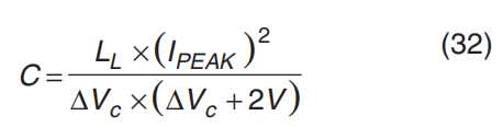
In the above equation, ∆Vc is equal to the acceptable change of voltage across the capacitor, usually between 40 and 60V.
在上面的等式中,∆Vc 等于电容器两端的可接受电压变化,通常在 40 到 60V 之间。
LL is equal to the leakage inductance of the transformer.
LL 等于变压器的漏感。
IPEAK is equal to the peak current in the inductor at the time of turn-off.
IPEAK 等于关断时电感中的峰值电流。
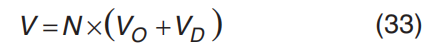
V is equal to the DC bias across the capacitor. This DC bias is a result of the DC path through the resistor and diode and the secondary side voltage reflected to the primary:
V 等于电容器两端的直流偏置。 这种直流偏置是通过电阻器和二极管的直流路径以及反射到初级的次级侧电压的结果:
The resistor is selected such that the RC time constant is much longer than the switching period. This resistor must not only dissipate the energy stored in the leakage inductance, but also the voltage due
to the DC bias of the capacitor:
电阻的选择应使 RC 时间常数比开关周期长得多。 该电阻器不仅要耗散漏电感中存储的能量,还要耗散由于漏感产生的电压。
到电容器的直流偏置:
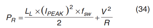
The resistor used on the demo board must dissipate 2.4W of power. The diode is selected based upon the charging current of the capacitor.
演示板上使用的电阻器必须消耗 2.4W 的功率。 根据电容器的充电电流选择二极管。
The secondary side of the converter requires an RC snubber across the diode (Figure 13) to damp the high frequency ringing on the 5V bus due to the parasitic inductance of the transformer and parasitic capacitance of the Schottky.
由于变压器的寄生电感和肖特基的寄生电容,转换器的次级侧需要二极管两端的 RC 缓冲器(图 13)来抑制 5V 总线上的高频振铃。
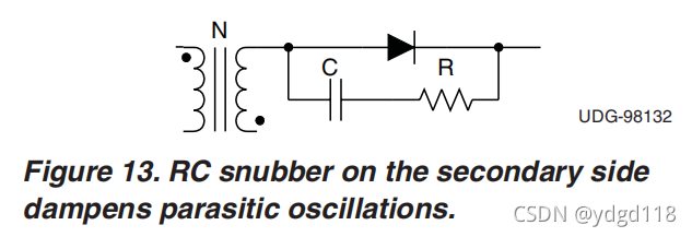 The capacitor is chosen such that, when placed across the Schottky, the oscillating frequency, fosc,is reduced by approximately half. The leakage inductance, LSL and parasitic capacitance, Cp can be determined by simultaneously solving (35a) and (35b)
选择电容器时,当跨过肖特基电容器放置时,振荡频率 fosc 减少大约一半。 可以通过同时求解 (35a) 和 (35b) 来确定电感的泄漏、LSL 和寄生电容 Cp。
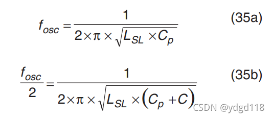 In (35b), C is the capacitor that was added to reduce the oscillation frequency. The appropriate value of the resistor is selected to provide critical damping to the oscillation:
在(35b)中,C 是为降低振荡频率而添加的电容器。 选择合适的电阻值来为振荡提供临界阻尼:
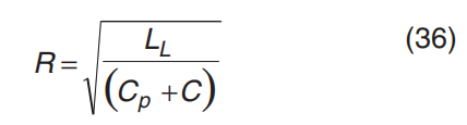
Because the time constant of this RC snubber is much less than the switching period but much longer than the voltage rise time, the power dissipated by the resistor is dependent upon the energy stored in the capacitor. Since the capacitor charges and discharges each cycle, the power the resistor must dissipate is equal to:
由于此 RC 缓冲器的时间常数远小于开关周期但远大于电压上升时间,因此电阻器消耗的功率取决于电容器中存储的能量。 由于电容器在每个周期充电和放电,因此电阻器必须消耗的功率等于:
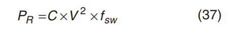
In (37), C is the RC snubber capacitor value. V is equal to the drain to source voltage reflected to the secondary side added to the output voltage plus the voltage drop across the diode. This snubber circuit will prevent the anode of the diode from ringing below the reverse voltage rating of the Schottky device.
在 (37) 中,C 是 RC 缓冲电容值。 V 等于反射到次级侧的漏源电压加上输出电压加上二极管两端的压降。 该缓冲电路将防止二极管的阳极在肖特基器件的反向电压额定值以下振铃。
7.LC FILTER LC滤波器
The voltage ripple on the output will occur at the switching frequency and is required to be less than 50mV peak to peak.
输出上的电压纹波将在开关频率下出现,并且要求峰峰值小于 50mV。
To meet the output noise specification, an LC filter was added to the converter output.
为满足输出噪声规范,转换器输出中增加了一个 LC 滤波器。
The unfiltered ripple, VR, will be equal to the peak secondary current multiplied by the ESR of the output capacitor bank.
未滤波的纹波 VR 将等于峰值次级电流乘以输出电容器组的 ESR。
The amount of attenuation needed to filter the ripple, VR, to an acceptable level is determined by (38)
将纹波 VR 过滤到可接受水平所需的衰减量由 (38) 确定

An LC filter will produce a gain plot with a –40dB/decade slope. The selected LC filter should have a pole that results in a minimum gain derived from (38) at the switching frequency. The pole frequency will occur at:
LC 滤波器将产生一个具有 –40dB/decade 斜率的增益图。 所选的 LC 滤波器应具有一个极点,该极点会导致在开关频率下从 (38) 得出的最小增益。 极点频率将出现在:
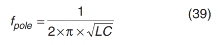
This design employs a 2mH iron powder toroid and a 33mF electrolytic capacitor for a pole frequency of 20kHz and a minimum gain of –8dB.
此设计采用 2mH 铁粉环形线圈和 33mF 电解电容器,极点频率为 20kHz,最小增益为 –8dB。


 651
651

 被折叠的 条评论
为什么被折叠?
被折叠的 条评论
为什么被折叠?
 到【灌水乐园】发言


