


ICAP原语的使用
一、杂谈
有一段时间没写博客了,因为从学校回家了。现在正值肺炎流行,不给社会添麻烦,自己在家调调程序看看论文。可是今天写的icap原语在板子上的验证没通过,因为学的是icap原语是用在S6芯片上的,但是因为自己回家没带S6的开发板,这里用7系列的icape2原语进行做实验,虽然板上验证没通过,但是还是非常用实用意义。最后在这个不平稳的日子里,希望武汉加油、中国加油、一起共度难关!!!
ICAP原语的介绍
ICAP原语是S6芯片上的一个原语,这里有必要对原语的概念说明一下,我们可以把原语想象成一个IP核,只不过IP核是图形化界面,而原语就相当于生成IP核生成的.v文件,原语的使用不需要添加相应的文件。对于ISE软件,原语调用的位置如下:
 其中对应的ICAP原语的调用位置如下:
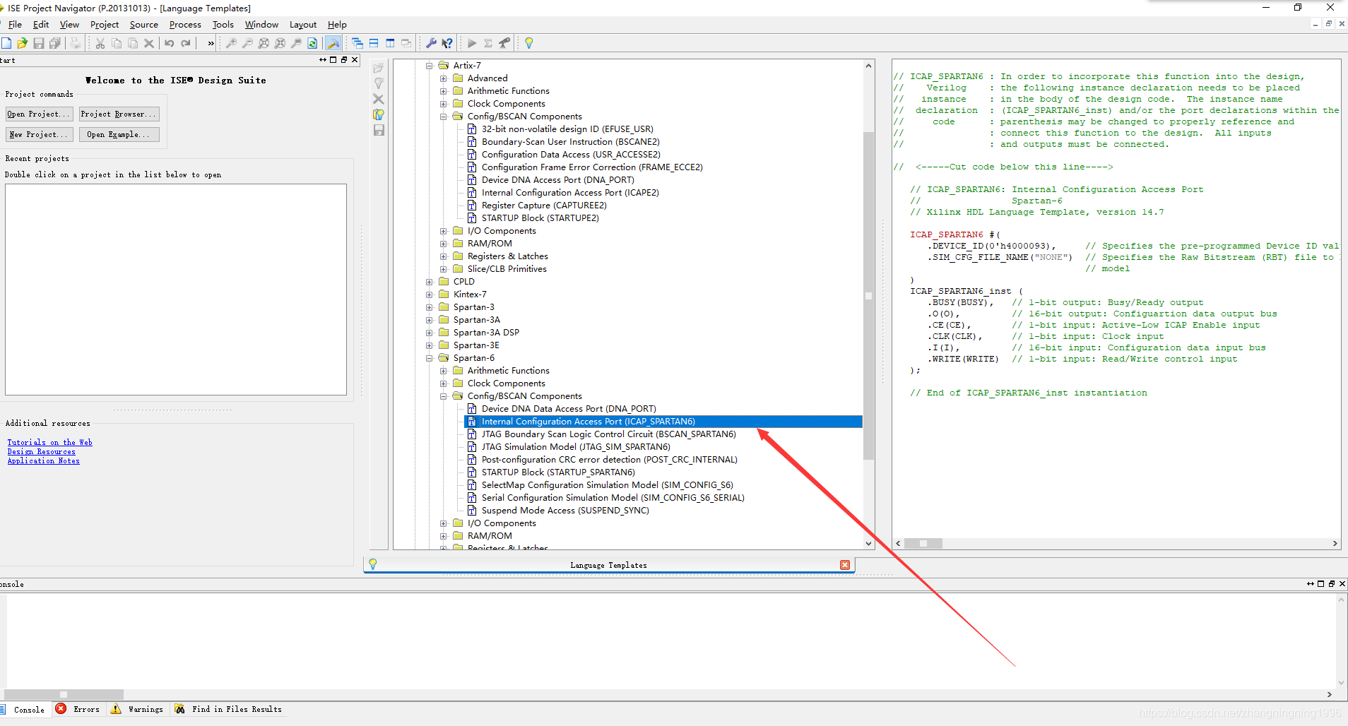
其中,icap原语的内容如下:
// ICAP_SPARTAN6 : In order to incorporate this function into the design,
//    Verilog    : the following instance declaration needs to be placed
//   instance    : in the body of the design code.  The instance name
//  declaration  : (ICAP_SPARTAN6_inst) and/or the port declarations within the
//     code      : parenthesis may be changed to properly reference and
//               : connect this function to the design.  All inputs
//               : and outputs must be connected.

//  <-----Cut code below this line---->

   // ICAP_SPARTAN6: Internal Configuration Access Port
   //                Spartan-6
   // Xilinx HDL Language Template, version 14.7

   ICAP_SPARTAN6 #(
      .DEVICE_ID(0'h4000093),     // Specifies the pre-programmed Device ID value
      .SIM_CFG_FILE_NAME("NONE")  // Specifies the Raw Bitstream (RBT) file to be parsed by the simulation
                                  // model
   )
   ICAP_SPARTAN6_inst (
      .BUSY(BUSY),   // 1-bit output: Busy/Ready output
      .O(O),         // 16-bit output: Configuartion data output bus
      .CE(CE),       // 1-bit input: Active-Low ICAP Enable input
      .CLK(CLK),     // 1-bit input: Clock input
      .I(I),         // 16-bit input: Configuration data input bus
      .WRITE(WRITE)  // 1-bit input: Read/Write control input
   );

   // End of ICAP_SPARTAN6_inst instantiation
这里对原语中得分几个信号的使用做出介绍:
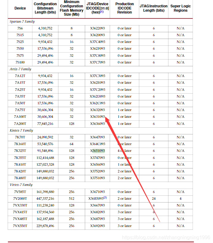
1、DEVICE_ID:不同芯片的DEVICE_ID不相同,在使用该原语时,一定要查找对用芯片的ID,具体查找的数据手册UG380 ;
2、SIM_CFG_FILE_NAME:仿真使用,默认即可。
3、BUSY:原语对应的忙信号
4、O:配置数据的输出
5、CE:原语的使能信号,低电平有效
6、CLK:原语的时钟信号
7、I:原语配置数据的输入信号
8、WRITE:读写原语的使能信号,低电平有效
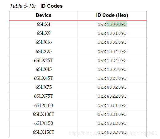
这里需要在DEVICE_ID中填入对应的ID号
然后按照上面的要求该原语得从I中输入相应的指令,FPGA才能从指定的存储地址启动。
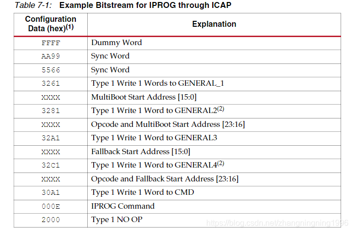
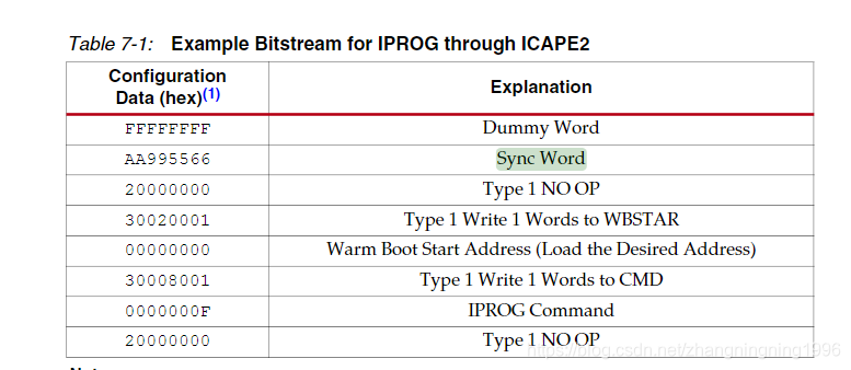
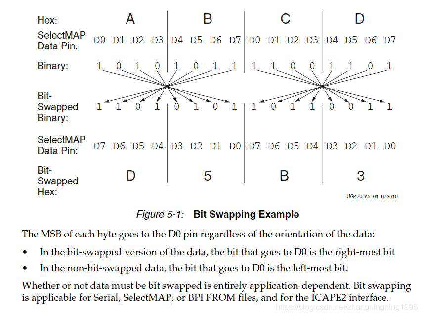
按照上面的数据输入到ICAP原语中,FPGA便可以从制定的存储器件指定的存储地址中读取代码,这里需要注意的是I中的数据与上表中的数据要按照字节反转,这部分内容在手册中也能查找到,如下:
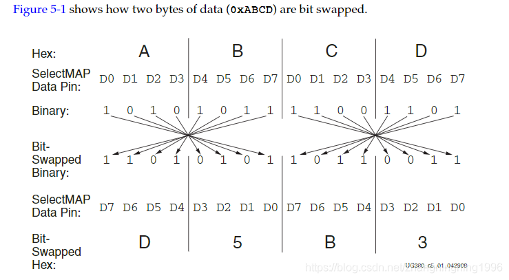
这里需要重点解释Opcode的含义,如下图:
该Opcode的物理意义是对用flash的读命令代码,对应镁光的一般是0x03。其余配置数据的含义从图中可以知道。有了以上信息,我们便可以操作S6系列的ICAP原语。
ICAPE2原语的介绍
由于在家没带S6的开发板,我们紧接着介绍A7开发板中ICAP原语的使用,通S6一样知道上述信息如下:
对于vivado软件,原语调用的位置如下:
其中对应的ICAP原语的调用位置如下: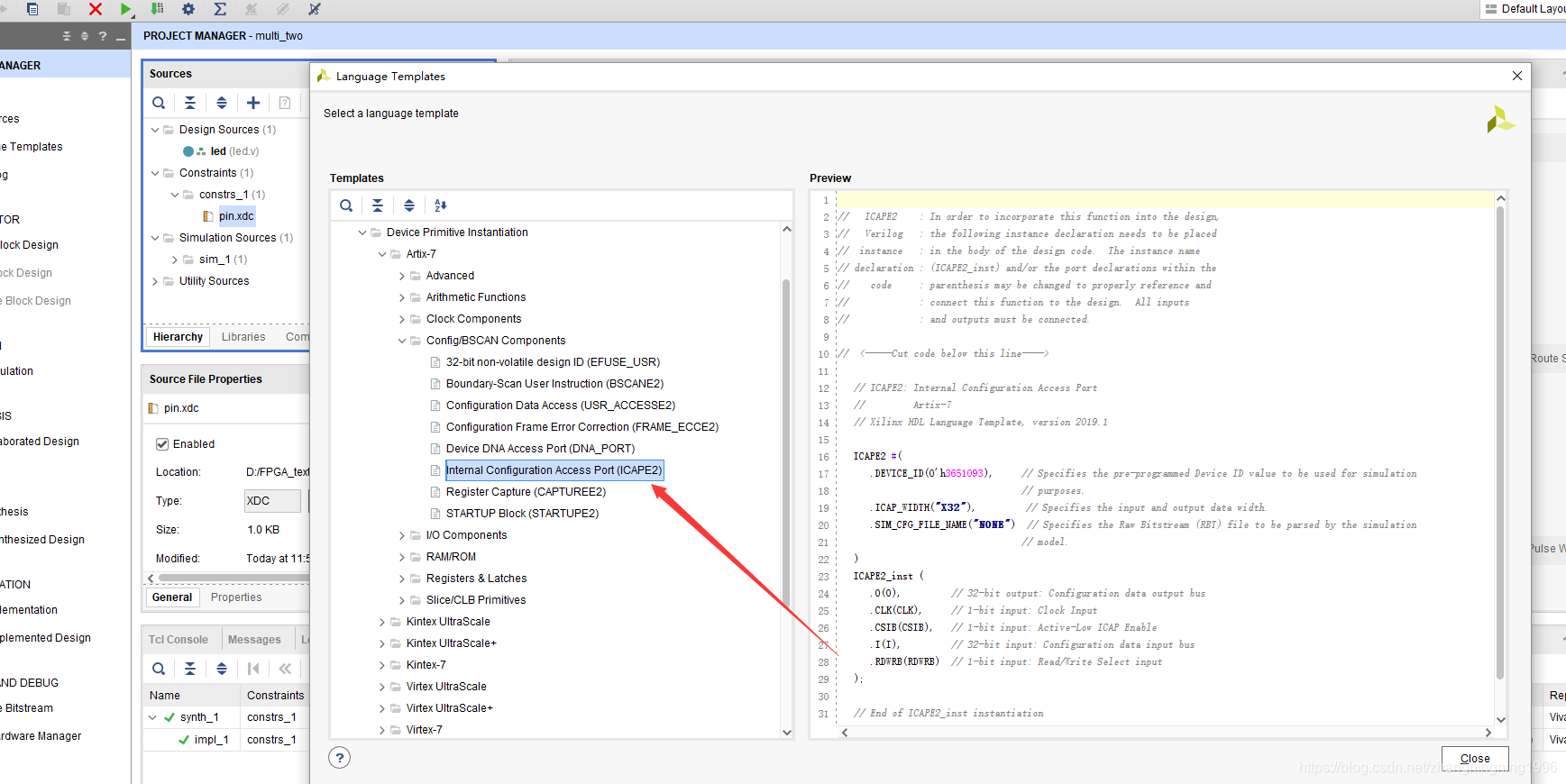
其中,icap原语的内容如下:
//   ICAPE2    : In order to incorporate this function into the design,
//   Verilog   : the following instance declaration needs to be placed
//  instance   : in the body of the design code.  The instance name
// declaration : (ICAPE2_inst) and/or the port declarations within the
//    code     : parenthesis may be changed to properly reference and
//             : connect this function to the design.  All inputs
//             : and outputs must be connected.

//  <-----Cut code below this line---->

   // ICAPE2: Internal Configuration Access Port
   //         Artix-7
   // Xilinx HDL Language Template, version 2019.1

   ICAPE2 #(
      .DEVICE_ID(0'h3651093),     // Specifies the pre-programmed Device ID value to be used for simulation
                                  // purposes.
      .ICAP_WIDTH("X32"),         // Specifies the input and output data width.
      .SIM_CFG_FILE_NAME("NONE")  // Specifies the Raw Bitstream (RBT) file to be parsed by the simulation
                                  // model.
   )
   ICAPE2_inst (
      .O(O),         // 32-bit output: Configuration data output bus
      .CLK(CLK),     // 1-bit input: Clock Input
      .CSIB(CSIB),   // 1-bit input: Active-Low ICAP Enable
      .I(I),         // 32-bit input: Configuration data input bus
      .RDWRB(RDWRB)  // 1-bit input: Read/Write Select input
   );

   // End of ICAPE2_inst instantiation
ICAPE2原语的代码
工程1的代码:
top模块的代码
`timescale 1ns / 1ps
// *********************************************************************************
// Project Name : OSXXXX
// Author       : zhangningning
// Email        : nnzhang1996@foxmail.com
// Website      :
// Module Name  : top.v
// Create Time  : 2020-01-29 13:45:19
// Editor       : sublime text3, tab size (4)
// CopyRight(c) : All Rights Reserved
//
// *********************************************************************************
// Modification History:
// Date             By              Version                 Change Description
// -----------------------------------------------------------------------
// XXXX       zhangningning          1.0                        Original
//
// *********************************************************************************


module top(
    input                   sclk            ,
    input                   rst_n           ,
    input                   key_i           ,
    output  wire    [ 3:0]  led
);

//========================================================================================\
//**************Define Parameter and  Internal Signals**********************************
//========================================================================================/
wire                        key_flag        ;

//========================================================================================\
//**************     Main      Code        **********************************
//=====================================================================================
最低0.47元/天 解锁文章


 3527
3527

 被折叠的 条评论
为什么被折叠?
被折叠的 条评论
为什么被折叠?
 到【灌水乐园】发言


