


A soft error is a temporary failure of a device caused by the effects of radiation on a silicon integrated circuit (Si ICs). Soft errors can affect the performance and reliability of equipment, especially in high-radiation environments such as space, defense, medical, and power systems.
As electronic devices continue to miniaturize and denser, the sensitivity of soft errors increases, because low-energy alpha particles can now flip a memory bit or change the timing of a logic circuit. One of the main sources of alpha particle radiation is the solder paste used to connect components in the package, which contains alpha radioactive elements.
Thanks to the use of flip-chip and the move to 3D packaging, solder bumps have moved so close to the moving silicon device that even low-energy alpha rays can cause soft errors. Therefore, it is necessary to develop Low Alpha activity Pb-free solders to reduce the occurrence of soft errors.
Alpha particle source of solder
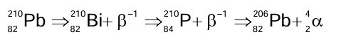
Lead-based solders are thought to be a major source of alpha particles, which was confirmed by a study conducted by the North Carolina Microelectronics Center (MCNC), which monitored alpha radiation at each step of the wafer bump process. The radioactivity of lead can be traced back to 238U. Starting at 238U, it decays to 210Pb, decays further to Bi in 22 years, then to Po, and again to 206Pb in 138 days. In addition to alpha particles, the decay process also involves the emission of beta particles (electrons). Beta particles have no effect on soft error. Uranium content in natural lead sources varies by as much as three orders of magnitude. During melting and chemical purification, although other elements may be removed, radioactive 210Pb is concentrated with non-radioactive 206Pb due to the same chemical properties of the two lead isotopes. In the 8 to 9 months after melting and purification, the α activity of lead can be as high as 100 α/ (cm2 "h).
Alpha particle production process:
Chip manufacturers usually divide the sources of alpha particles into internal and external sources.
a) Intrinsic source refers to a source that is present in the processed silicon itself, but is usually less important. They are caused by process-related factors, such as residues left by phosphoric acid etching. Phosphoric acid is commonly used in the patterning of silicon nitride insulation films in wafer fabrication. It is usually relatively low in purity and contains low levels of radioactive isotopes. Other intrinsic sources include trace impurities in film oxides and nitrides, extraneous impurities added to the silicon during implantation operations, and impurities in the silicon wafer itself.
b) External source: The external source is usually different from the silicon chip, but within the integrated circuit package. Most sources of alpha particles fall into this category. Table 1 lists the most common sources of alpha particles in microelectronic packaging. Table 2 lists individual contribution estimates for some of these alpha particle emission sources. It is currently believed that almost all materials used for integrated circuit packaging will cause soft error failure. Due to size reduction, distance reduction, and increasing sensitivity of devices to SER, it is necessary to develop routine monitoring procedures for incoming materials and manufacturing processes.
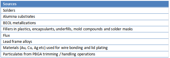
Table 1. The most common sources of alpha particles in microelectronic packaging
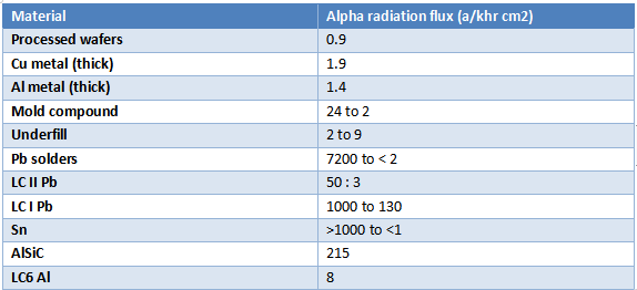
Table 2. Alpha radiation activity of some common materials used in microelectronic packaging
Development and application of low alpha particle solder paste
In order to reduce the alpha particle activity in the solder paste, there are two main methods: one is to use lead-free solder, and the other is to use low alpha activity lead solder. Lead-free solder refers to the solder with no lead or very low lead content, they are usually composed of tin, silver, copper and other elements. The advantage of lead-free solder is that it can avoid the harm of lead to the environment and the human body, while also eliminating the source of alpha particles in the solder paste.
Low alpha active lead solder refers to the lead solder that has been specially treated to remove 210Pb of radioactivity. This treatment method usually consists of two steps: one is the use of high-purity raw materials, and the other is the use of vacuum or inert gas environment for melting and purification. This can effectively reduce the activity of α particles in the solder paste to less than 0.01α / (cm2 "h). The advantage of low α-active lead solder is that it can maintain the excellent properties of lead solder, such as low melting point, low oxidation, low creep, low intermetallic compound formation rate, etc., and can also reduce the occurrence of soft errors.
At present, the low alpha activity lead-free solder paste has been used in some high-end microelectronics packaging fields, such as space, defense, medical and power systems. These areas have very high reliability requirements for equipment, and can not tolerate any soft errors. Therefore, the use of low alpha activity lead-free solder paste can effectively improve the radiation resistance and safety of the equipment.
Fuinda low alpha particle solder
The Low Alpha solder series is a high lead solder with low alpha particle count developed by Fuyinda for high density and miniaturization packages such as SiP system level package and Flip Chip chip flip. It is used in mobile communication (smartphones, tablets, wearable devices), Internet of Things (Wi-Fi, BLTE,UWB,LTE-M & NB-IoT, consumer, industrial), automotive (infotainment systems), high-performance computing (computing, networking, artificial intelligence) and other fields.
Fuinda's low alpha products include low alpha (<0.01 cph/cm2) and ultra low alpha (<0.002cph/cm2) radiation levels, lead-free, high lead alloys, and particle size models covering T3, T4, T5, T6. The low α solder series has the advantages of good spherical tin powder, narrow particle size distribution, low oxygen content, high chemical purity, meet the requirements of α particle radiation specifications, and can provide customized development services. Welcome to inquire.


 606
606

 被折叠的 条评论
为什么被折叠?
被折叠的 条评论
为什么被折叠?
 到【灌水乐园】发言


