


文章目录
一、3-8译码器的实验与仿真
1.logisim绘制3-8译码器
利用logisim绘制出3-8译码器电路如下:

其真值表如下:
| A2 | A1 | A0 | B7 | B6 | B5 | B4 | B3 | B2 | B1 | B0 |
|---|---|---|---|---|---|---|---|---|---|---|
| 0 | 0 | 0 | 0 | 0 | 0 | 0 | 0 | 0 | 0 | 1 |
| 0 | 0 | 1 | 0 | 0 | 0 | 0 | 0 | 0 | 1 | 0 |
| 0 | 1 | 0 | 0 | 0 | 0 | 0 | 0 | 1 | 0 | 0 |
| 0 | 1 | 1 | 0 | 0 | 0 | 0 | 1 | 0 | 0 | 0 |
| 1 | 0 | 0 | 0 | 0 | 0 | 1 | 0 | 0 | 0 | 0 |
| 1 | 0 | 1 | 0 | 0 | 1 | 0 | 0 | 0 | 0 | 0 |
| 1 | 1 | 0 | 0 | 1 | 0 | 0 | 0 | 0 | 0 | 0 |
| 1 | 1 | 1 | 1 | 0 | 0 | 0 | 0 | 0 | 0 | 0 |
2.quartus软件利用verilog语言生成RTL电路并实现仿真
1)verilog实现三八译码器代码如下
module three_to_eight(
	a,
	b,
	c,
	out
);
input a; //输入端口a
input b; //输入端口b
input c; //输入端口c
output [7:0]out;//输出端口out

reg [7:0]out;
always@(a,b,c)
begin
	case({a,b,c})
	3'b000:out = 8'b0000_0001;
	3'b001:out = 8'b0000_0010;
	3'b010:out = 8'b0000_0100;
	3'b011:out = 8'b0000_1000;
	3'b100:out = 8'b0001_0000;
	3'b101:out = 8'b0010_0000;
	3'b110:out = 8'b0100_0000;
	3'b111:out = 8'b1000_0000;
	endcase
end
endmodule
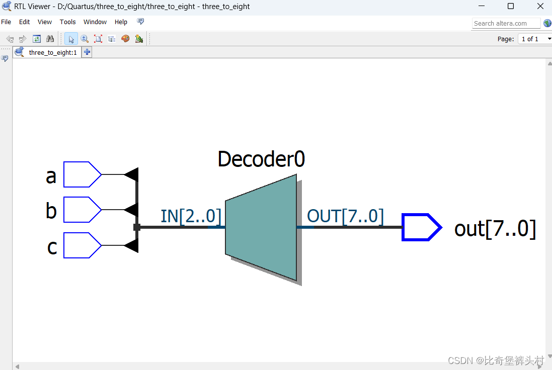
2)生成的RTL电路
3)quartus电路仿真结果
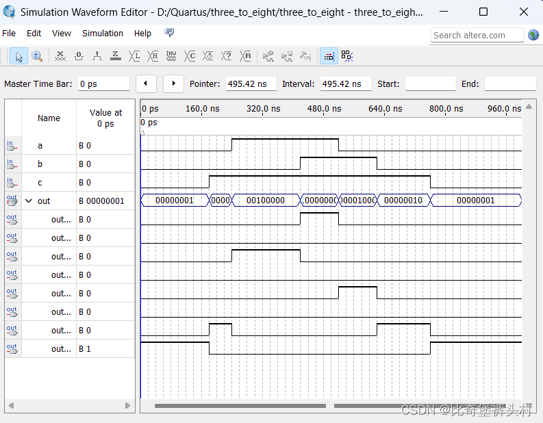
仿真结果正确,仿真正确
4)modelsim电路仿真结果
仿真文件如下:
timescale 1ns/1ns

 module three_to_eight_tb();

 reg  a;

 reg  b;

 reg  c;

 wire   [7:0]   out;


 initial    begin
    a <= 1'b1;
    b <= 1'b0;
    c <= 1'b1;

 end

 //a:产生随机数,模拟 a 的输入情况

 always #10 a <= {$random} % 2;

 //b:产生随机数,模拟 b 的输入情况

 always #10 b <= {$random} % 2;

 //c:产生随机数,模拟c 的输入情况

 always #10 c <= {$random} % 2;


 initial begin

    $timeformat(-9, 0, "ns", 6);

    $monitor("@time %t:a=%b b=%b c=%b out=%b",$time,a,b,c,out);

 end


 three_to_eight three_to_eight_ins

 (

    .a(a),
    .b(b),
    .c(c),
    .out(out)

 );

 endmodule
仿真结果如下:
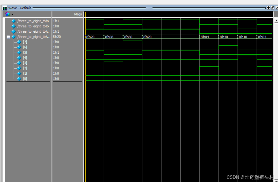
仿真结果正确,仿真正确
5)问题分析
1.Verilog 综合生成的3-8译码器电路原理图与原始设计电路存在什么差异? 仿真测试生成的结果是否与真值表一致?
答:verilog综合生成的电路将内部的基本门电路进行封装,只通过输入与输出来观察相应的功能,简化了操作;仿真测试生成的结果与真值表一致。
2.Verilog代码设计的3-8译码器模块的输出信号 为何要定义为 reg类型而不用默认wire(导线)类型?改成wire型是否可以?
答:wire型数据常用来表示以assign关键字指定的组合逻辑信号,模块的输入输出端口类型都默认为wire型,wire相当于物理连线,默认初始值是z(高组态)。reg型表示的寄存器类型,用于always模块内被赋值的信号,必须定义为reg型,代表触发器,常用于时序逻辑电路,reg相当于存储单元,默认初始值是x(未知状态)。三八译码器中使用always语句是过程赋值应该使用reg类型的输出模块,若替换成wir类型会发生错误。
二、全加器电路实验
1.一位全加器
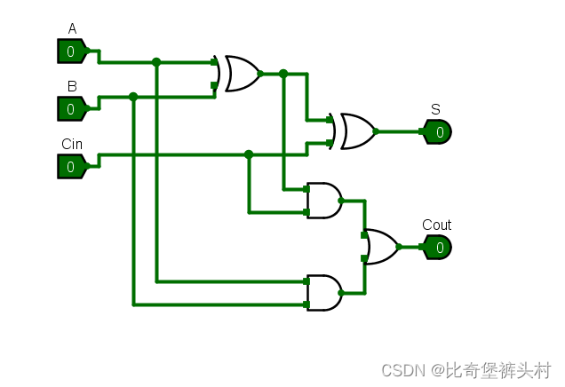
1)门级描述
verilog代码如下:
module ad_1(A,B,cin,sum,cout);
	input A,B,cin;
	output sum,cout;
	wire t1,t2,t3,t4;
	and U1(t1,A,B);
	and U2(t2,A,cin);
	and U3(t3,B,cin);
	or U4(cout,t1,t2,t3);
	xor U5(t4,A,B);
	xor U6(sum,t4,cin);
endmodule
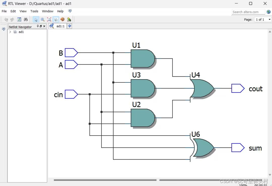
RTL电路如下:
logisim电路如下:
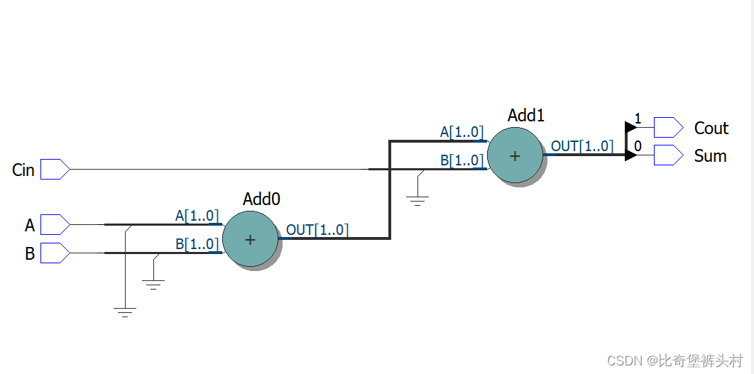
2)行为级描述
verilog代码如下:
module ad_12 (
  input A, B, Cin,
  output Sum, Cout

);
  assign {Cout, Sum} = A + B + Cin;
endmodule
RTL电路如下:
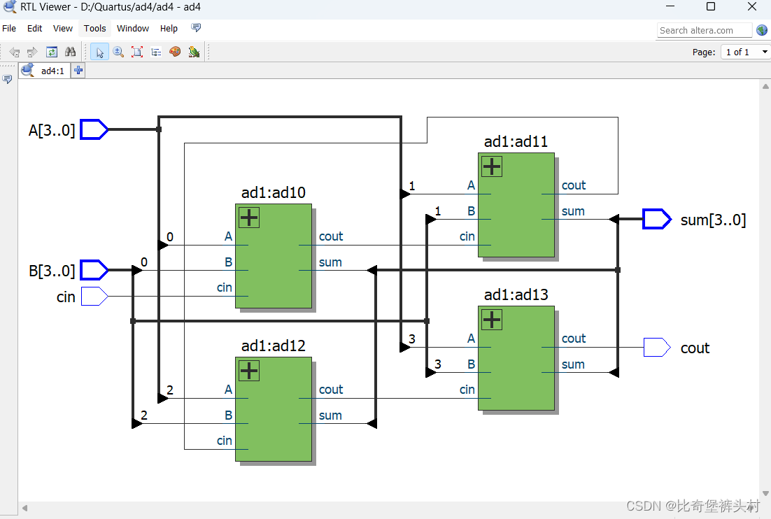
2.四位全加器
1)门级描述
verilog代码如下:
module ad1(A,B,cin,sum,cout);
input A,B,cin;
output sum,cout;
wire t1,t2,t3,t4;
and U1(t1,A,B);
and U2(t2,A,cin);
and U3(t3,B,cin);
or U4(cout,t1,t2,t3);
xor U5(t4,A,B);
xor U6(sum,t4,cin);
endmodule
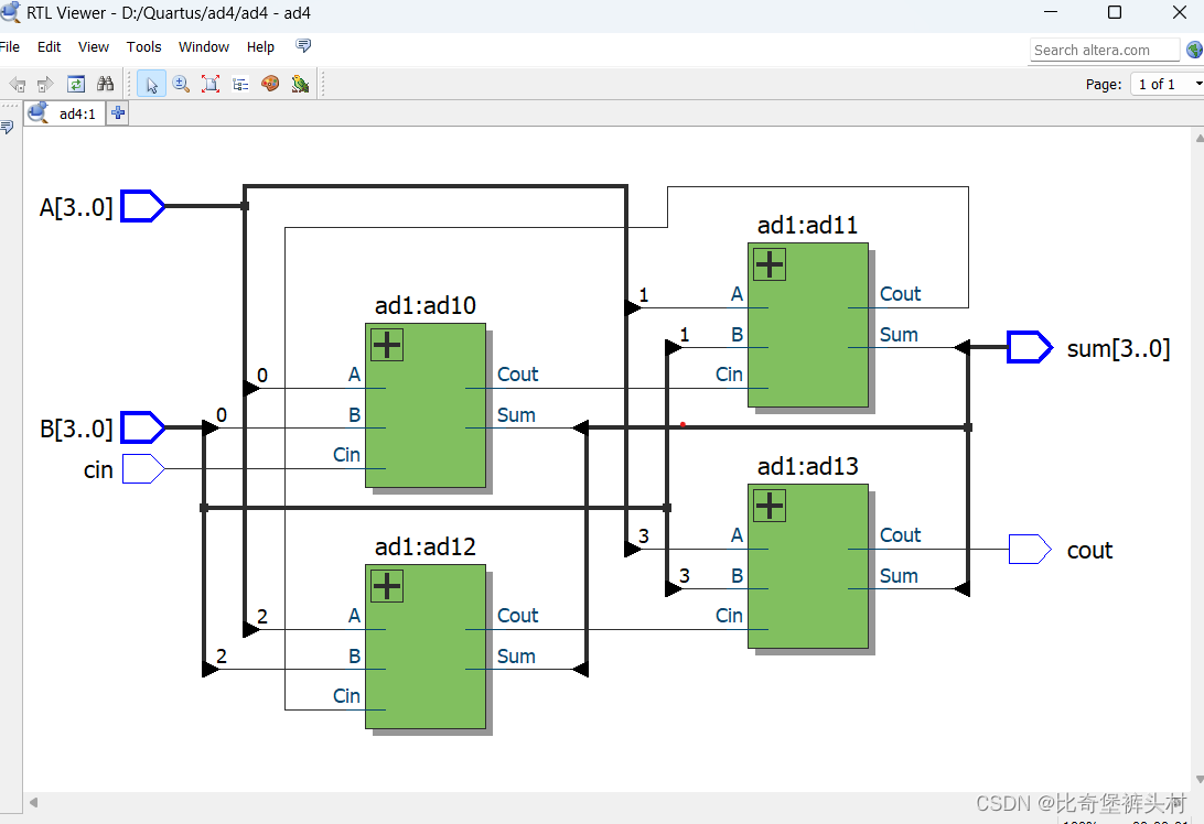
module ad4
(
input [3:0]A,B,
input cin,
output [3:0]sum,
output cout
);
wire[4:0]c;
assign c[0] = cin;
ad1 ad10(A[0],B[0],c[0],sum[0],c[1]);
ad1 ad11(A[1],B[1],c[1],sum[1],c[2]);
ad1 ad12(A[2],B[2],c[2],sum[2],c[3]);
ad1 ad13(A[3],B[3],c[3],sum[3],c[4]);
assign cout = c[4];
endmodule
RTL电路如下:
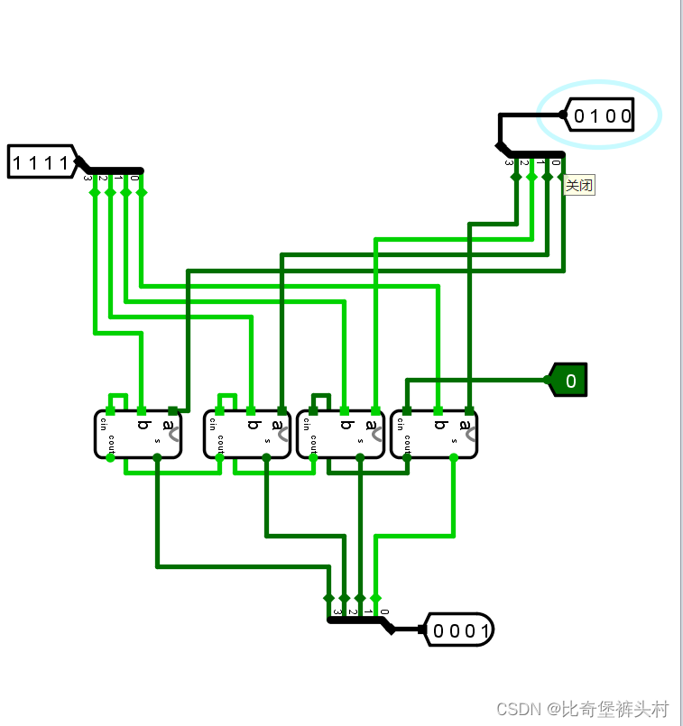
logisim电路如下:
2)行为级描述
verilog代码如下:
module ad1 (
  input A, B, Cin,
  output Sum, Cout

);
  assign {Cout, Sum} = A + B + Cin;
endmodule


module ad4
(
	input [3:0]A,B,
	input cin,
	output [3:0]sum,
	output cout
);
	wire[4:0]c;
	assign c[0] = cin;
	ad1 ad10(A[0],B[0],c[0],sum[0],c[1]);
	ad1 ad11(A[1],B[1],c[1],sum[1],c[2]);
	ad1 ad12(A[2],B[2],c[2],sum[2],c[3]);
	ad1 ad13(A[3],B[3],c[3],sum[3],c[4]);
	assign cout = c[4];
endmodule
RTL电路如下:
3.八位全加器
verilog代码如下:
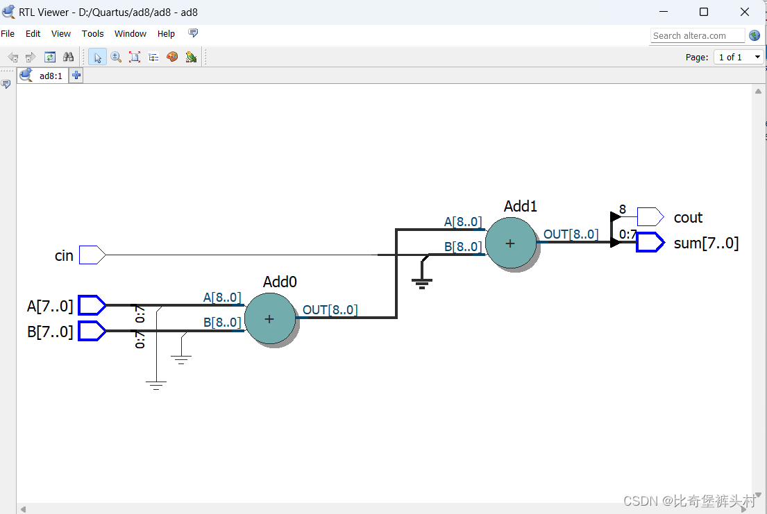
module ad8 (
  input [7:0] A, B,
  input cin,
  output[7:0]sum,
  output cout

);
  assign {cout, sum} = A + B + cin;
endmodule
RTL电路如下:
三、16位ALU(算术逻辑单元)的电路设计
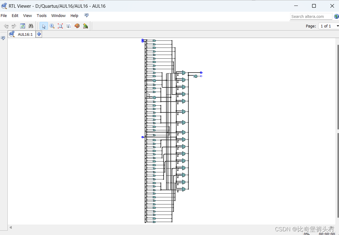
1.verilog语言实现及其RTL电路
module ALU16 (
    input [15:0] operand_A,
    input [15:0] operand_B,
    input [2:0]  opcode,  // 0: ADD, 1: SUB, 2: AND, 3: OR, 4: XOR, 5: NOT
    output reg [15:0] result,
    output reg zero_flag
);

always @* begin
    case(opcode)
        3'b000: result = operand_A + operand_B;      // 加法
        3'b001: result = operand_A - operand_B;      // 减法
        3'b010: result = operand_A & operand_B;      // 与
        3'b011: result = operand_A | operand_B;      // 或
        3'b100: result = operand_A ^ operand_B;      // 或非
        3'b101: result = ~operand_A;                 // 非
        default: result = 16'b0;                     // Default case (optional)
    endcase

    // Set zero_flag
    zero_flag = (result == 16'b0);
end

endmodule
在这个模块中,operand_A和operand_B是输入的16位操作数,opcode是控制ALU执行哪种操作的3位输入。result是16位输出,表示ALU的计算结果。zero_flag表示结果是否为零,如果为零则置1,否则置0。
2.仿真测试
仿真文件:
`timescale 1ns/1ps

module ALU16_tb;

  // Inputs
  reg [15:0] operand_A;
  reg [15:0] operand_B;
  reg [2:0]  opcode;

  // Outputs
  wire [15:0] result;
  wire zero_flag;

  // Instantiate the ALU module
  ALU16 uut (
    .operand_A(operand_A),
    .operand_B(operand_B),
    .opcode(opcode),
    .result(result),
    .zero_flag(zero_flag)
  );

  // Stimulus generation
  initial begin
    // Test case 1: ADD
    operand_A = 8'b11001100;
    operand_B = 8'b00110011;
    opcode = 3'b000;
    #10;

    // Test case 2: SUB
    operand_A = 8'b11001100;
    operand_B = 8'b00110011;
    opcode = 3'b001;
    #10;

    // Test case 3: AND
    operand_A = 8'b11001100;
    operand_B = 8'b00110011;
    opcode = 3'b010;
    #10;

    // Test case 4: OR
    operand_A = 8'b11001100;
    operand_B = 8'b00110011;
    opcode = 3'b011;
    #10;

    // Test case 5: XOR
    operand_A = 8'b11001100;
    operand_B = 8'b00110011;
    opcode = 3'b100;
    #10;

    // Test case 6: NOT
    operand_A = 8'b11001100;
    opcode = 3'b101;
    #10;

    $stop;
  end

endmodule
仿真结果:
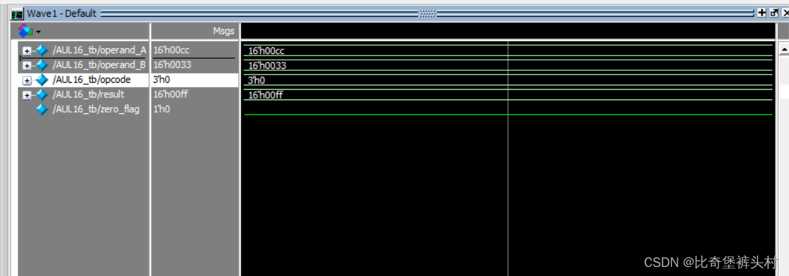


 2603
2603


 被折叠的 条评论
为什么被折叠?
被折叠的 条评论
为什么被折叠?
 到【灌水乐园】发言


