


文章目录
一、前言
HDLBits是一个很棒的 Verilog 学习网站。
HDLBits 在提供 Verilog 基础语法教程的同时,还能够在线仿真你的 Verilog 模块,将你的输出与正确的时序比较。
可以让初学者在快速上手的同时,也更直观的感受到这门语言的特殊之处
下面是传送门:
HDLBits
二、组合逻辑相关练习
1.2 多路复用器
问题描述:
Create a one-bit wide, 2-to-1 multiplexer. When sel=0, choose a. When sel=1, choose b.
代码:
module top_module(
    input a, b, sel,
    output out );
     assign out = (sel) ? b : a;

endmodule
仿真结果:

1.2 全加器
问题描述:
Create a full adder. A full adder adds three bits (including carry-in) and produces a sum and carry-out.
代码:
module top_module(
    input a, b, cin,
    output cout, sum );
    assign{cout,sum} = a + b + cin;
endmodule

1.3 卡诺图
问题描述:
Consider the function f shown in the Karnaugh map below.
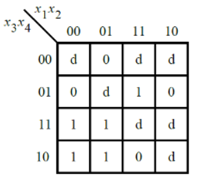
Implement this function. d is don’t-care, which means you may choose
to output whatever value is convenient.
代码:
module top_module (
    input [4:1] x,
    output f );
    assign f = (~x[1] & x[3]) | (x[1] & x[2] & ~x[3]);
endmodule
二、门电路相关练习
2.1 非门
Create a module that implements a NOT gate.
This circuit is similar to wire, but with a slight difference. When
making the connection from the wire in to the wire out we’re going to
implement an inverter (or “NOT-gate”) instead of a plain wire.Use an assign statement. The assign statement will continuously drive
the inverse of in onto wire out.

代码:
module top_module( input in, output out );
	assign out=~in;
endmodule

2.2 与门
Create a module that implements an AND gate.
This circuit now has three wires (a, b, and out). Wires a and b already have values driven onto them by the input ports. But wire out currently is not driven by anything. Write an assign statement that drives out with the AND of signals a and b.
Note that this circuit is very similar to the NOT gate, just with one more input. If it sounds different, it’s because I’ve started describing signals as being driven (has a known value determined by something attached to it) or not driven by something. Input wires are driven by something outside the module. assign statements will drive a logic level onto a wire. As you might expect, a wire cannot have more than one driver (what is its logic level if there is?), and a wire that has no drivers will have an undefined value (often treated as 0 when synthesizing hardware).

代码:

2.3 或非门
Create a module that implements a NOR gate. A NOR gate is an OR gate with its output inverted. A NOR function needs two operators when written in Verilog.
An assign statement drives a wire (or “net”, as it’s more formally called) with a value. This value can be as complex a function as you want, as long as it’s a combinational (i.e., memory-less, with no hidden state) function. An assign statement is a continuous assignment because the output is “recomputed” whenever any of its inputs change, forever, much like a simple logic gate.

module top_module(
    input a,
    input b,
    output out );
	assign out=~(a|b);
endmodule

三、关于时序逻辑的练习
3.1 D触发器
A D flip-flop is a circuit that stores a bit and is updated periodically, at the (usually) positive edge of a clock signal.
D flip-flops are created by the logic synthesizer when a clocked always block is used (See alwaysblock2). A D flip-flop is the simplest form of “blob of combinational logic followed by a flip-flop” where the combinational logic portion is just a wire.
Create a single D flip-flop.
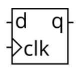
module top_module (
    input clk,    // Clocks are used in sequential circuits
    input d,
    output reg q );//

    // Use a clocked always block
    //   copy d to q at every positive edge of clk
    //   Clocked always blocks should use non-blocking assignments
    always@(posedge clk) begin
        q <= d;
    end
endmodule

3.2 D锁存器
Implement the following circuit:
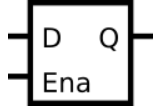
Note that this is a latch, so a Quartus warning about having inferred a latch is expected.
代码:
module top_module (
    input d,
    input ena,
    output q);
    always@(*)begin
        if(ena)begin
            q<=d;
        end
    end

endmodule
3.3 1~12的计数器
Design a 1-12 counter with the following inputs and outputs:
Reset Synchronous active-high reset that forces the counter to 1
Enable Set high for the counter to run
Clk Positive edge-triggered clock input
Q[3:0] The output of the counter
c_enable, c_load, c_d[3:0] Control signals going to the provided 4-bit counter, so correct operation can be verified.
You have the following components available:
the 4-bit binary counter (count4) below, which has Enable and synchronous parallel-load inputs (load has higher priority than enable). The count4 module is provided to you. Instantiate it in your circuit.
logic gates
module count4(
input clk,
input enable,
input load,
input [3:0] d,
output reg [3:0] Q
);
The c_enable, c_load, and c_d outputs are the signals that go to the internal counter’s enable, load, and d inputs, respectively. Their purpose is to allow these signals to be checked for correctness.
代码:
module top_module (
    input clk,
    input reset,
    input enable,
    output [3:0] Q,
    output c_enable,
    output c_load,
    output [3:0] c_d
); //

    count4 the_counter (clk, c_enable, c_load, c_d /*, ... */ );
    reg [3:0] temp;

    //4-bit计数器的控制信号
    assign c_enable = enable;
    //带复位和置位,
    assign c_load   = reset | (Q == 4'd12 & enable == 1'b1);
    assign c_d      = 4'b1;

//    count4 the_counter (clk, c_enable, c_load, c_d, Q );
    count4 Inst_count4
    (
        .clk(clk),
        .enable(c_enable),
        .load(c_load),
        .d(c_d),
        .Q(Q)
    );
endmodule

四、总结
本次实验目的是利用HDLBits网站做对verilog的再次练习。通过此次练习我不仅掌握了verilog的语法,还了解了它与硬件的交互方式,了解了一些电路的设计过程,为以后的学习打下了基础。


 937
937


 被折叠的 条评论
为什么被折叠?
被折叠的 条评论
为什么被折叠?
 到【灌水乐园】发言


