


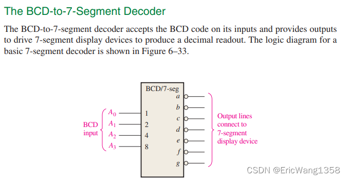
A decoder is a digital circuit that detects the presence of a specified combination of bits (code) on its inputs and indicates the presence of that code by a specified output level.
In its general form, a decoder has n input lines to handle n bits and from one to 2n output lines to indicate the presence of one or more n-bit combinations.
In this section, three fixed-function IC decoders are introduced. The basic principles can be extended to other types of decoders.
解码器是一种数字电路,它检测其输入上的指定比特(编码)组合的存在,并通过指定的输出电平指示该编码的存在。在一般形式下,解码器有 n 个输入线来处理 n 位,并有从一个到 2^n 个输出线来指示一个或多个 n 位组合的存在。在本节中,介绍了三种固定功能的集成电路解码器。这些基本原理可以扩展到其他类型的解码器。
完成本节后,您应该能够:
- 定义解码器
- 设计一个逻辑电路来解码任意比特组合
- 描述74HC154二进制到十进制解码器
- 扩展解码器以适应更大数量的比特编码
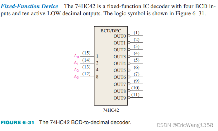
- 描述74HC42BCD到十进制解码器
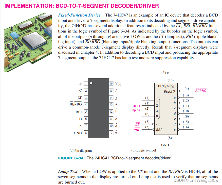
- 描述74HC47BCD到7段数码管解码器
- 讨论7段数码管显示器中的零抑制
The Basic Binary Decoder
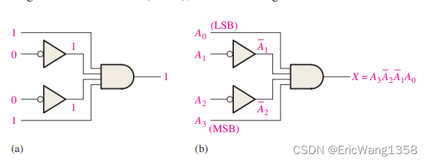
Suppose you need to determine when a binary 1001 occurs on the inputs of a digital circuit. An AND gate can be used as the basic decoding element because it produces a HIGH output only when all of its inputs are HIGH. Therefore, you must make sure that all of the inputs to the AND gate are HIGH when the binary number 1001 occurs; this can be done by inverting the two middle bits (the 0s), as shown in Figure 6–26
假设您需要确定数字电路的输入中是否出现了二进制数1001。AND门可以用作基本的解码元素,因为它只有在所有输入都为高电平时才会产生高电平输出。因此,当二进制数1001出现时,您必须确保AND门的所有输入都为高电平;这可以通过反转两个中间位(0)来实现,如图6-26所示。
In the representation of a binary number or other weighted code in this book, the LSB is the right-most bit in a horizontal arrangement and the topmost bit in a vertical arrangement, unless specified otherwise.
If a NAND gate is used in place of the AND gate in Figure 6–26, a LOW output will indicate the presence of the proper binary code, which is 1001 in this case.
The 4-Bit Decoder
为了解码四位所有可能的组合,需要十六个解码门($2^4 = 16$)。这种类型的解码器通常被称为4线到16线解码器,因为有四个输入和十六个输出,或者称为1-of-16解码器,因为对于输入上的任何给定编码,十六个输出中的一个被激活。十六个二进制编码及其相应的解码功能的列表如表6-4所示。
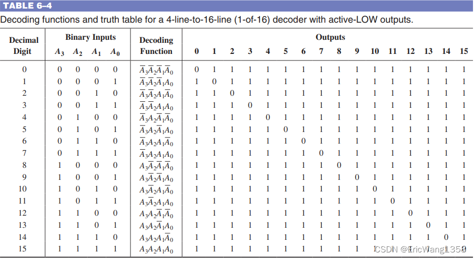
If an active-LOW output is required for each decoded number, the entire decoder can be implemented with NAND gates and inverters. In order to decode each of the sixteen binary codes, sixteen NAND gates are required (AND gates can be used to produce active-HIGH outputs).
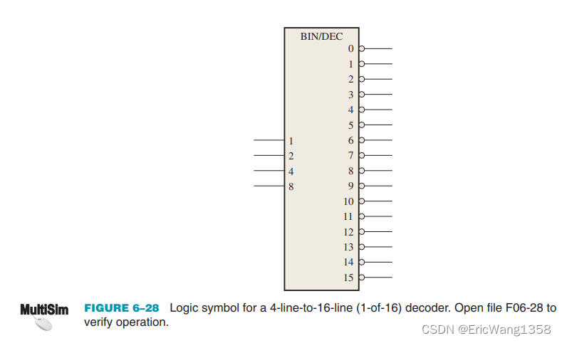
A logic symbol for a 4-line-to-16-line (1-of-16) decoder with active-LOW outputs is shown in Figure 6–28. The BIN/DEC label indicates that a binary input makes the corresponding decimal output active.
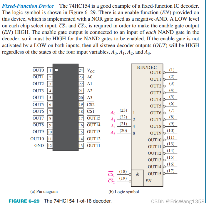
在74HC154中,使能引脚(EN)通过一个逻辑门(NOR门)来控制。这个逻辑门的输出连接到解码器的每个NAND门的一个输入上。当使能引脚(EN)为低电平时,逻辑门的输出为高电平,这个高电平会传递到每个NAND门中,使得每个NAND门都能工作。因此,只有当使能引脚(EN)为低电平时,解码器的输出才会根据输入变量(A0、A1、A2、A3)的状态进行解码,并产生相应的输出信号。如果使能引脚(EN)为高电平,则逻辑门的输出为低电平,传递到每个NAND门中的信号也为低电平,这样所有的NAND门都会停止工作,解码器的输出将保持高电平。
(要使得EN的输出为High,High 给到所有out判断(NAND),才能正常工作)
此处注意&是表示OR, >=1 才是And
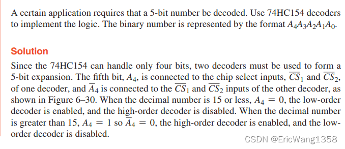
两个解码器中的一个被用于表示小于或等于15的数字,另一个被用于表示大于15的数字。这样,两个解码器结合起来可以表示0到31之间的32个数字。
The BCD-to-Decimal Decoder
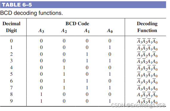
he BCD-to-decimal decoder converts each BCD code (8421 code) into one of ten possible decimal digit indications. It is frequently referred as a 4-line-to-10-line decoder or a 1-of-10 decoder. The method of implementation is the same as for the 1-of-16 decoder previously discussed, except that only ten decoding gates are required because the BCD code represents only the ten decimal digits 0 through 9. A list of the ten BCD codes and their corresponding decoding functions is given in Table 6–5. Each of these decoding functions is implemented with NAND gates to provide active-LOW outputs. If an active-HIGH output is required, AND gates are used for decoding. The logic is identical to that of the first ten decoding gates in the 1-of-16 decoder (see Table 6–4).
BCD到十进制解码器将每个BCD码(8421码)转换为十个可能的十进制数字指示之一。它通常被称为4线到10线解码器或1选10解码器。其实现方法与前面讨论的1选16解码器相同,只是因为BCD码只表示十进制数字0到9,所以只需要十个解码门。
这十个BCD码及其对应的解码功能的列表如表6-5所示。每个解码功能都是使用NAND门实现的,以提供低电平输出。如果需要高电平输出,则使用AND门进行解码。这种逻辑与1选16解码器中的前十个解码门的逻辑相同。
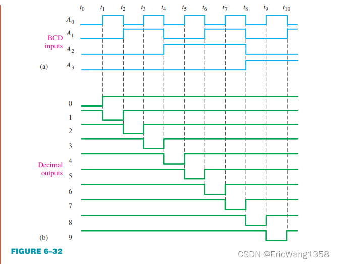
 If the input waveforms in Figure 6–32(a) are applied to the inputs of the 74HC42, show the output waveforms
(回顾:占空比(duty cycle):占空比是指信号的高电平时间与一个周期的比率。在时序图中,如果需要确定占空比,通常会查看信号的高电平和低电平的宽度,然后计算高电平时间与一个周期的比率。这个比率就是信号的占空比。)

for common-cathode:所有LED的阴极都连接在一起接地, 阳极不同。


 972
972


 被折叠的 条评论
为什么被折叠?
被折叠的 条评论
为什么被折叠?
 到【灌水乐园】发言


