


Introduction
from: https://en.wikipedia.org/wiki/Process_corners
In semiconductor manufacturing, a process corner is an example of a design-of-experiments (DoE) technique that refers to a variation of fabrication parameters used in applying an integrated circuit design to a semiconductor wafer. Process corners represent the extremes of these parameter variations within which a circuit that has been etched onto the wafer must function correctly. A circuit running on devices fabricated at these process corners may run slower or faster than specified and at lower or higher temperatures and voltages, but if the circuit does not function at all at any of these process extremes, the design is considered to have inadequate design margin.[1]
To verify the robustness of an integrated circuit design, semiconductor manufacturers will fabricate corner lots, which are groups of wafers that have had process parameters adjusted according to these extremes, and will then test the devices made from these special wafers at varying increments of environmental conditions, such as voltage, clock frequency, and temperature, applied in combination (two or sometimes all three together) in a process called characterization. The results of these tests are plotted using a graphing technique known as a shmoo plot that indicates clearly the boundary limit beyond which a device begins to fail for a given combination of these environmental conditions.
Corner-lot analysis is most effective in digital electronics because of the direct effect of process variations on the speed of transistor switching during transitions from one logic state to another, which is not relevant for analog circuits, such as amplifiers.
Types of corners
When working in the schematic domain, we usually only work with front end of line (FEOL) process corners as these corners will affect the performance of devices. But there is an orthogonal set of process parameters that affect back end of line (BEOL) parasitics.
FEOL corners
One naming convention for process corners is to use two-letter designators, where the first letter refers to the N-channel MOSFET (NMOS) corner, and the second letter refers to the P channel (PMOS) corner. In this naming convention, three corners exist: typical, fast and slow. Fast and slow corners exhibit carrier mobilities that are higher and lower than normal, respectively. For example, a corner designated as FS denotes fast NFETs and slow PFETs.
There are therefore five possible corners: typical-typical (TT) (not really a corner of an n vs. p mobility graph, but called a corner, anyway), fast-fast (FF), slow-slow (SS), fast-slow (FS), and slow-fast (SF). The first three corners (TT, FF, SS) are called even corners, because both types of devices are affected evenly, and generally do not adversely affect the logical correctness of the circuit ==> with proper external conditions that is. The resulting devices can function at slower or faster clock frequencies, and are often binned as such. The last two corners (FS, SF) are called "skewed" corners, and are cause for concern. This is because one type of FET will switch much faster than the other, and this form of imbalanced switching can cause one edge of the output to have much less slew than the other edge. Latching devices may then record incorrect values in the logic chain.
==> "slew" : from TI
Slew rate is defined as the maximum rate of change of an op amps output voltage, and is given in units of volts per microsecond. Slew rate is measured by applying a large signal step, such as one volt, to the input of the op amp, and measuring the rate of change from 10% to 90% of the output signal's amplitude.
BEOL corners
In addition to the FETs themselves, there are more on-chip variation (OCV) effects that manifest themselves at smaller technology nodes (==> according to the linked video below, 90nm and below). These include process, voltage and temperature (PVT) variation effects on on-chip interconnect, as well as via structures.
Extraction tools often have a nominal corner to reflect the nominal cross section of the process target. Then the corners cbest and cworst (which were the only essential feature for older processes) were created to model the smallest and largest cross sections that are in the allowed process variation. A simple thought experiment shows that the smallest cross section with the largest vertical spacing will produce the smallest coupling capacitance. CMOS Digital circuits were more sensitive to capacitance than resistance so this variation was initially acceptable. As processes evolved and resistance of wiring became more critical, the additional rcbest and rcworst were created to model the minimum and maximum cross sectional areas for resistance. But the one change is that cross sectional resistance is not dependent on oxide thickness (vertical spacing between wires) so for rcbest the largest is used and for rcworst the smallest is used.
Recommended Readings
below are llinks to 2 rather well made short yet comprehensive summaries, including basic backgrounds for Process Corners and RC Corners:
You Don't Know About The Process Corners in VLSI Design ?
You Don't Know About The RC Corners in VLSI Design ?
Terms and Elaboration
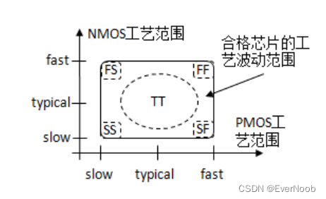
1、工艺角(Process Corner)
与双极晶体管不同,在不同的晶片之间以及在不同的批次之间,MOSFETs 参数变化很
大。为了在一定程度上减轻电路设计任务的困难,工艺工程师们要保证器件的性能在某
个范围内。 如果超过这个范围,就将这颗IC报废了,通过这种方式来保证IC的良率。
传统上,提供给设计师的性能范围只适用于数字电路并以“工艺角”(Process Corners)的形式给出。其思想是:把NMOS和PMOS晶体管的速度波动范围限制在由四个角所确定的矩形内。这四个角分别是:快NFET和快PFET,慢NFET和慢PFET,快NFET和慢PFET,慢NFET和快PFET。例如,具有较薄的栅氧、较低阈值电压的晶体管,就落在快角附近。从晶片中提取与每一个角相对应的器件模型时,片上NMOS和PMOS的测试结构显示出不同的门延迟,而这些角的实际选取是为了得到可接受的成品率。因此,只有满足这些性能的指标的晶片才认为是合格的。在各种工艺角和极限温度条件下对电路进行仿真是决定成品率的基础。
graph from Corner芯片TT,FF,SS_别想太多的博客-CSDN博客_tt ff ss
工艺角分析,corner analysis,一般有五种情况:
==> the the 2 letter are descriptions in the order of N-P(mos)
fast nmos and fast pmos (ff)
slow nmos and slow pmos (ss)
slow nmos and fast pmos (sf)
fast nmos and slow pmos (fs)
typical nmos and typical pmos (tt)
t,代表typical (平均值)
s,代表slow(电流小)
f,代表fast(电流大)
PVT (process, voltage, temperature)
设计除了要满足上述5个corner外,还需要满足电压与温度等条件, 形成的组合称为PVT (process, voltage, temperature) 条件。电压如:1.0v+10% ,1.0v ,1.0v-10% ; 温度如:-40C, 0C 25C, 125C。
==> 1. the V here is obviously for operational Voltage
==> 2. P is for Process Parameters, which includes (from linked video above):
设计时设计师还常考虑找到最好最坏情况. 时序分析中将最好的条件(Best Case)定义为速度最快的情况, 而最坏的条件(Worst Case)则相反。根据不同的仿真需要,会有不同的PVT组合。以下列举几种标准STA分析条件[16]:
WCS (Worst Case Slow) : slow process, high temperature, lowest voltage

TYP (typical) : typical process, nominal temperature, nominal voltage

BCF (Best Case Fast ) : fast process, lowest temperature, high voltage

WCL (Worst Case @ Cold) : slow process, lowest temperature, lowest voltage
在进行功耗分析时,可能是另些组合如:
ML (Maximal Leakage ) : fast process, high temperature, high voltage

TL (typical Leakage ) : typical process, high temperature, nominal voltage
OCV (On-chip Variations)
由于偏差的存在,不同晶圆之间,同一晶圆不同芯片之间,同一芯片不同区域之间情况都是不相同的。造成不同的因素有很多种,这些因素造成的不同主要体现:
1,IR Drop造成局部不同的供电的差异;

2,晶体管阈值电压的差异;

3,晶体管沟道长度的差异;

4,局部热点形成的温度系数的差异;

5,互连线不同引起的电阻电容的差异。
OCV可以描述PVT在单个芯片所造成的影响。更多的时候, 用来考虑长距离走线对时钟路径的影响。在时序分析时引入derate参数模拟OCV效应,其通过改变时延迟的早晚来影响设计。
三种STA(Static Timing Analysis)分析方法:
1,单一模式, 用同一条件分析setup/hold ;

2,WC_BC模式, 用worst case计算setup,用best case计算hold;

3,OCV模式, 计算setup 用计算worst case数据路径,用best case计算时钟路径;
计算hold 用best case计算数据路径,用worst case计算时钟路径;

Extension 1 setup/hold vs. wc/bc
Setup and Hold Time_EverNoob的博客-CSDN博客_violated setup和hold
==> why wc for setup, while bc for hold???
Extension 2 SSTA (Statistical Static Timing Analysis)
from 工艺角,PVT, TT,SS,FF,FS,SF_白山头的博客-CSDN博客
统计静态时序分析
全局工艺差异(global_process_variations), 也称为片间器件差异(inter-die device variations), 描述同一器件不同芯片间的差异。同一芯片的器件应用同一参数,器件的不同参数是相互独立的,而且每个参数都是呈统计分布的。==> i.e. even though we set the process parameters, P, the same for a certain chip, the manufactured devices will inevitably display statistically regular variation due to manufacturing defects and techinical limitations.
局部工艺差异(local_process_variations), 也称为片内器件差异 (intra-die devicevariations), 描述同一器件在同一芯片不同区域的差异。每个差异也是呈统计分布的。
也就是说对于某一个全局参数,应该细化成多个局部参数,每个局部参数都是呈统计分布的。如果提供的库是基于局部参数差异统计建立起来的,在进行基于OCV模型的静态时序分析时,就无需OCV参数的设定。
对于互连线差异也是一样的.决定同一段线的因素有很多种,比如线宽,厚度,介电系数,刻蚀等,但同一因素不同区域是不相同的,各个因素之间也是相互独立的。这些差异同样需要进行统计学概括。
...
基于这样的观点,同一时序路径可能存在不同种情况的组合,而且每种情况的参数都是呈统计学分布,组合的计算将不是单纯的相加差,而是需要相关性分析与统计学计算。统计方法的引入,改变了传统静态时序分析悲观但不实际的做法。
Complexity of Process Corners in Advanced Nodes (< 7nm)
"At 7nm and below, modeling what will actually show up in silicon is a lot more complicated."
“When the foundry refers to the timing goal, it means you need to hit the timing of the paths within 10% of, let’s say, the actual number,” Abadir said. “There is about 10% or 15% slack, depending on the maturity of the process, depending on things like how much yield they are hoping to get. In the final month or two of tapeout, the design team will start running the higher end corners that are very aggressive to see if these corners will take what they designed. They take the same design that they had, run the extraction against this worst case corner. They will also re-do the timing, re-do the power calculation, and see what happens to these numbers. If it’s way off, they start working on which ones are causing the problem and may tweak them. They try to do as much as they can in the last couple of months. It’s a matter of positioning and allowing a little bit of margin to see how far they are if the worst case conditions from the process variations happen, but it is a very non-scientific endeavor.”
Nevertheless, it’s also an essential endeavor. “We need to ensure our designs are manufacturable and demonstrate the required performance across manufacturing variability of advanced node processes,” said Sunil Bhardwaj
Advanced challenges for leading edge
Indeed, advanced nodes such as 7nm and below have made it that much more challenging to account for the corners in a design. “For interconnect corners, there was a large increase with the advent of multi-patterning,” Robertson said. “With multi-patterning, you know have geometries on the same layer represented in different masks, which means not only is there inter-layer variation (as has always been the case), but you know have intra-layer variation due to mask shifts. Anytime you introduce more processing steps or add layers there is an opportunity for variation that needs to be captured in a model or, potentially, in the description of another corner.”


 1万+
1万+

 被折叠的 条评论
为什么被折叠?
被折叠的 条评论
为什么被折叠?
 到【灌水乐园】发言


