


说明
新设计了1个KU040 FPGA板子,回来之后接上JTAG FPGA不识别。做如下检查:
1、电源测试点均正常;
2、查看贴片是否有漏焊,检查无异常,设计上NC的才NC;
3、反复检查JTAG接线是否异常,贴片是否异常;
上述检查均无问题,开始查看原理图,逐个对照XILINX手册进行研究。 https://www.amd.com/content/dam/xilinx/support/documents/user_guides/ug570-ultrascale-configuration.pdf
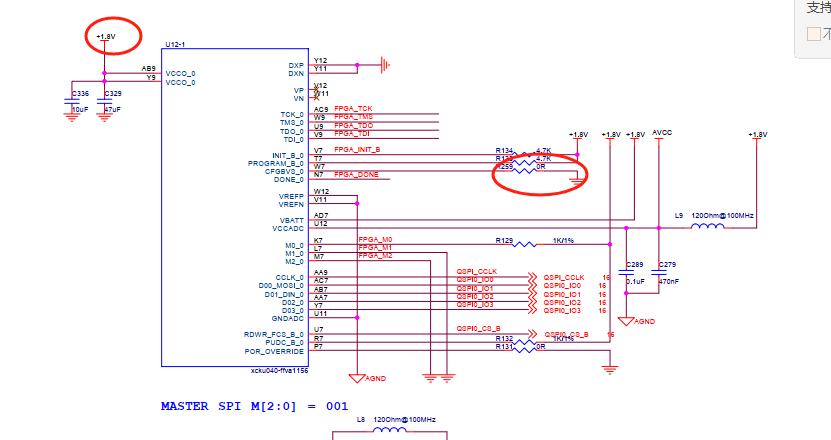
其中发现 CFGBVS 在设计图中接了地,对照XILINX 手册
In the Kintex UltraScale and Virtex UltraScale FPGAs, the configuration banks voltage select
(CFGBVS) pin must be set to High or Low to determine the I/O voltage support for the pins
in bank 0, and for the multi-function pins in bank 65 when they are used during
configuration. The CFGBVS is a logic input pin referenced between VCCO_0 and GND. When
the CFGBVS pin is connected to the VCCO_0 supply of 3.3V or 2.5V, the configuration I/O
support operation at 3.3V or 2.5V. When the CFGBVS pin is connected to GND, the
configuration I/O support operation at 1.8V or 1.5V. There is no CFGBVS pin in the Artix
UltraScale+, Kintex UltraScale+, and Virtex UltraScale+ FPGAs because their configuration
I/O only support operation at 1.8V or 1.5V.

Configuration is not supported below the minimum recommended operating voltage for
1.5V as specified in the data sheet. The CFGBVS pin setting determines the I/O voltage
support for bank 0 at all times, before, during, and after configuration. CFGBVS similarly
controls the voltage tolerance on bank 65, but only during configuration.
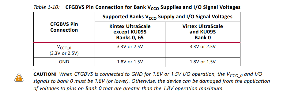
也就是说,这里原理图 CFGBVS 接地肯定是不对的,必须拉高到3.3V,还好留了1个0欧姆电阻在这里 还可以飞线补救一下。


 2719
2719


 被折叠的 条评论
为什么被折叠?
被折叠的 条评论
为什么被折叠?
 到【灌水乐园】发言


