


本文仅供学习,不作任何商业用途,严禁转载。绝大部分资料来自----数字集成电路——电路、系统与设计(第二版)及中国科学院段成华教授PPT
超大规模集成电路设计----基本概念(二)
- 简短的历史回顾(A Brief Historical Perspective)
- 纳米时代的设计挑战(Design Challenges in Nanoscale Era)
- Design Abstraction and Representation
- Y-Chart-Based Structured Design Concept
- IC Design Flows
- Design Automation Tools
- Quality Metrics of Digital Design
简短的历史回顾(A Brief Historical Perspective)
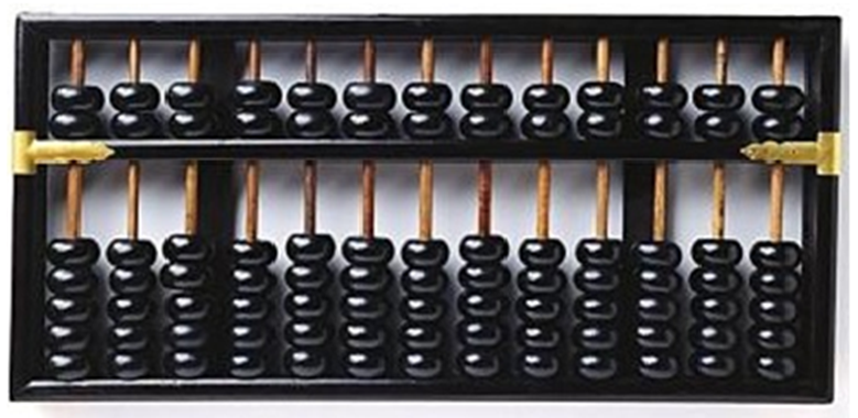
中国已知最早的计算设备–算盘(Abacus)
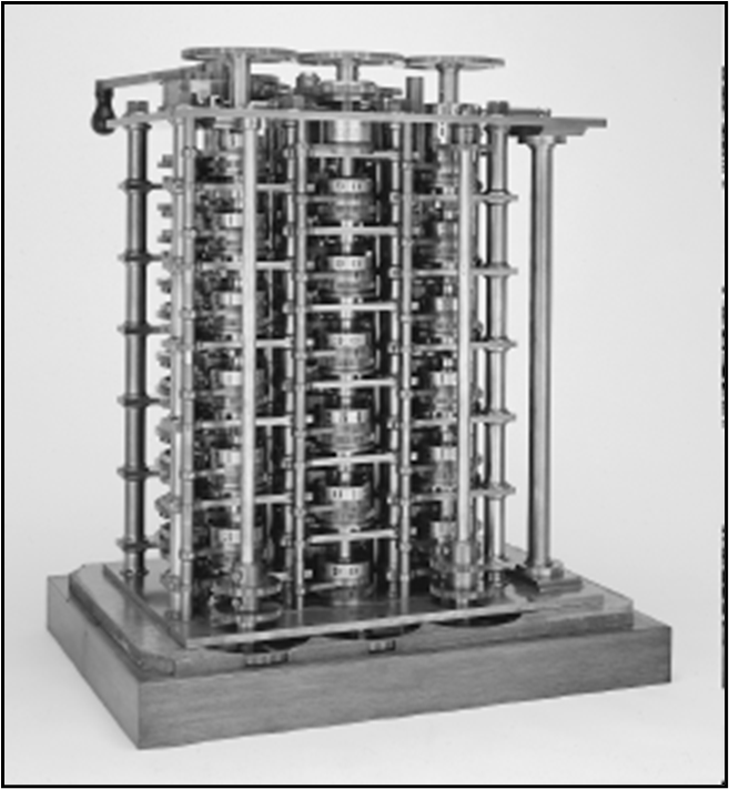
世界上最早的自动计算器
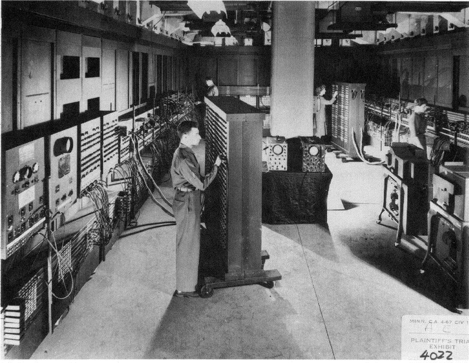
基于真空管的计算机时代:ENIAC
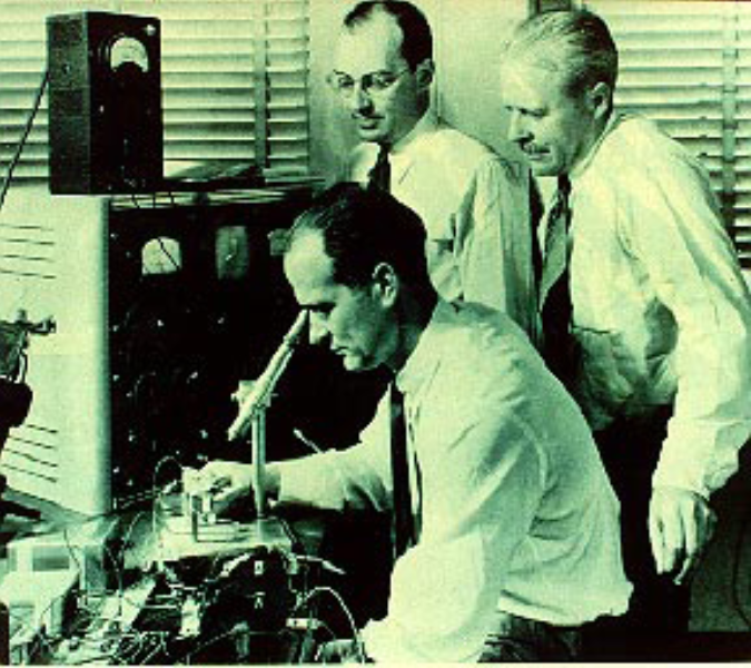
晶体管的发明-1947 Schockley等

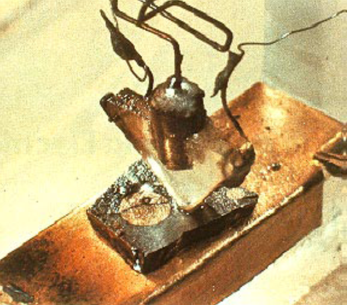
第一块集成电路-1958(锗geermanium) Kilby等
Noyce independently built the first IC on silicon.
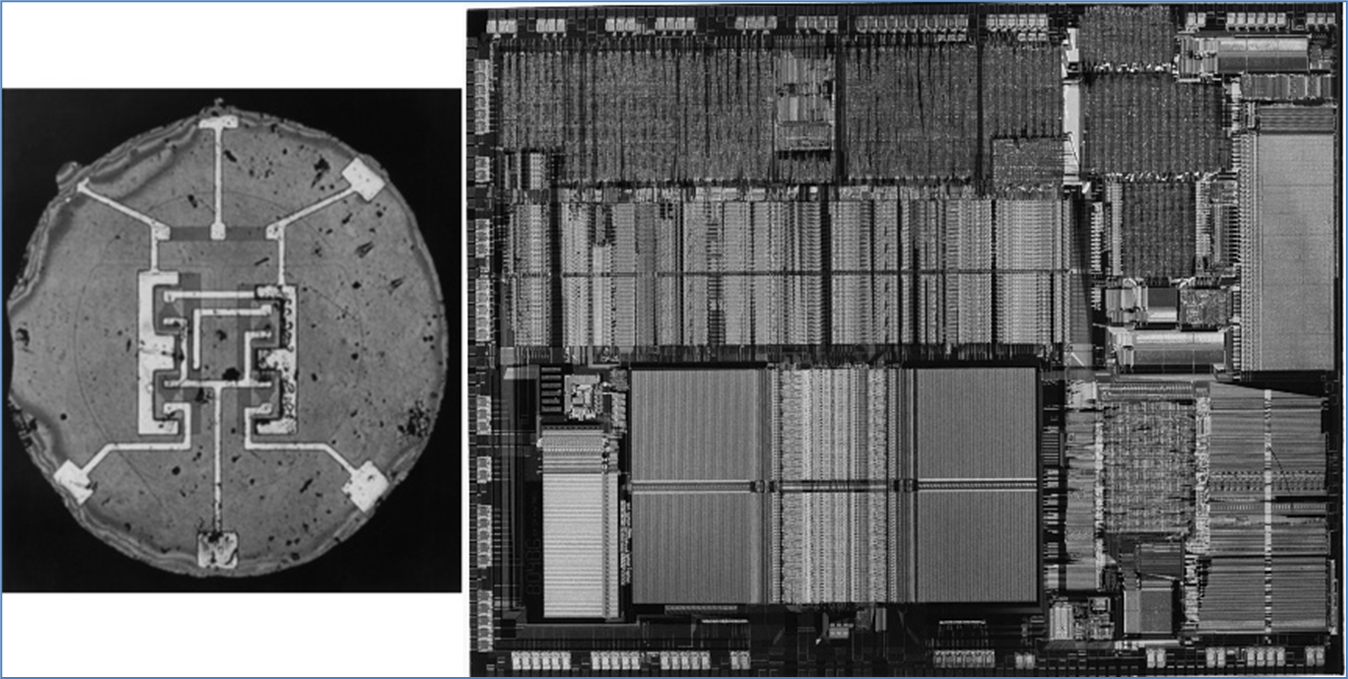
20世纪60年代初(左)和90年代初(右)制造的最先进的IC显微照片。20世纪60年代的IC包含四个双极晶体管和几个电阻器。20世纪90年代的芯片包含超过一百万个MOS晶体管。
第一个数字逻辑门和TTL(The First Digital Logic Gate and TTL)
- 第一个数字逻辑门:第一个数字逻辑门由Harris于1956年推出的分立元件制成。
- 第一个商用的逻辑门:J. Kilby的工作产生了1960年第一套IC商用逻辑门(Fairchild Micro-logic系列)。
- TTL:第一个真正成功的 IC 逻辑系列 TTL 出现在 1962 年;它非常成功,直到 20 世纪 80 年代为止,它在数字半导体市场中占据了最大的份额。
MOSFET
- 基本原理的提出:
Proposed in a patent by J. Lilienfeld (Canada) in1925, and independently, by O. Heil in England in 1935; - PMOS-only logic:
The first practical IC in 1960s; Frank Wanlass at Fairchild in 1963 described a logic gate using MOSFET; - NMOS-only logic:
Intel 4004 (1972, 7 μm),
8080 (1974, 6 μm); - CMOS (Complementary MOS) IC: Late 1970s up to now (7 nm,5 nm, 3 nm).
80486 (1990, 0.8 μm),
Pentium Pro (1995, 0.35 μm),
Core i7 (2011, 32 nm).
摩尔定律(The Moore’s Law, 1965)
摩尔定律在摩尔写的论文中的原话:组件成本的复杂性以每年大约两倍的速度增加。当然,在短期内,这一比率即使不增加,也有望继续下去。从长远来看,增长率更加不确定,尽管没有理由相信它不会在至少10年内保持几乎不变。这意味着到1975年,每个集成电路的最低成本组件数量将达到65,000个。
设计演示(Designs Demo)
IBM’s PowerPC chip (1998, 0.25 μm)
纳米时代的设计挑战(Design Challenges in Nanoscale Era)
1.尺寸和工具(Scales and Tools)
“Our ability as humans to shape and control the environment around us has improved steadily over time, most dramatically in the past 100 years. "随着时间的推移,我们塑造和控制周围环境的能力稳步提高,在过去 100 年中表现最为显著。
“The degree of control is reflected in the scale (size) at which objects can be constructed, which is governed by the tools available for constructing them.”控制程度反映在可以构建对象的比例(大小)上,而规模(大小)则由可用于构建它们的工具控制。
2.IC设计的复杂性(The Complexity of IC Design)
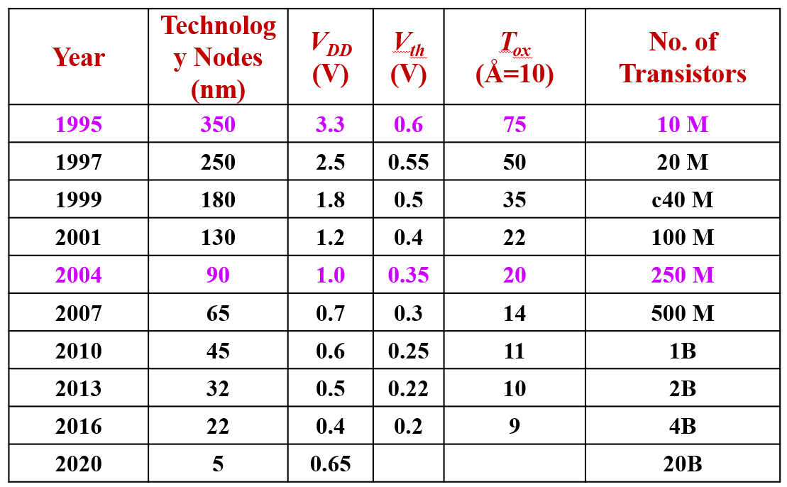
随着IC制造技术的缩小,==最小特征尺寸(minimum feature sizes)==正在接近10纳米领域。 挑战是众多而艰巨的。
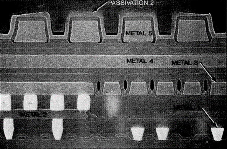
层间约束(Interlayer Constraints)
集成电路的层间约束是指在芯片制造过程中,不同的材料介质层之间需要满足的一些条件,以保证芯片的正常工作和可靠性。这些条件包括:
层间对齐:每一层的图案需要与下一层的图案精确地对齐,以避免电路的断路或短路。
层间隔离:每一层的材料需要与其他层的材料有足够的隔离,以防止电流的泄漏或干扰。
层间连接:每一层的电路需要与其他层的电路有有效的连接,以实现芯片的功能和性能。
层间厚度:每一层的材料需要有合适的厚度,以保证芯片的结构强度和电学特性。
集成电路的层间约束是芯片设计和制造的重要因素,它们影响着芯片的尺寸、速度、功耗、成本等指标。随着芯片技术的发展,层间约束也在不断变化和优化,以适应更高的集成度和更复杂的功能。
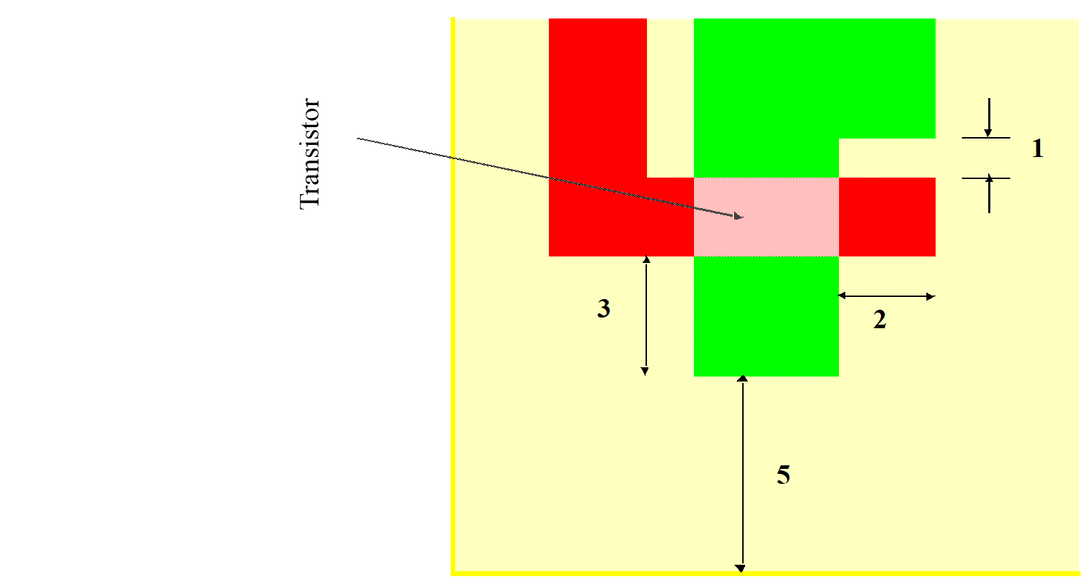
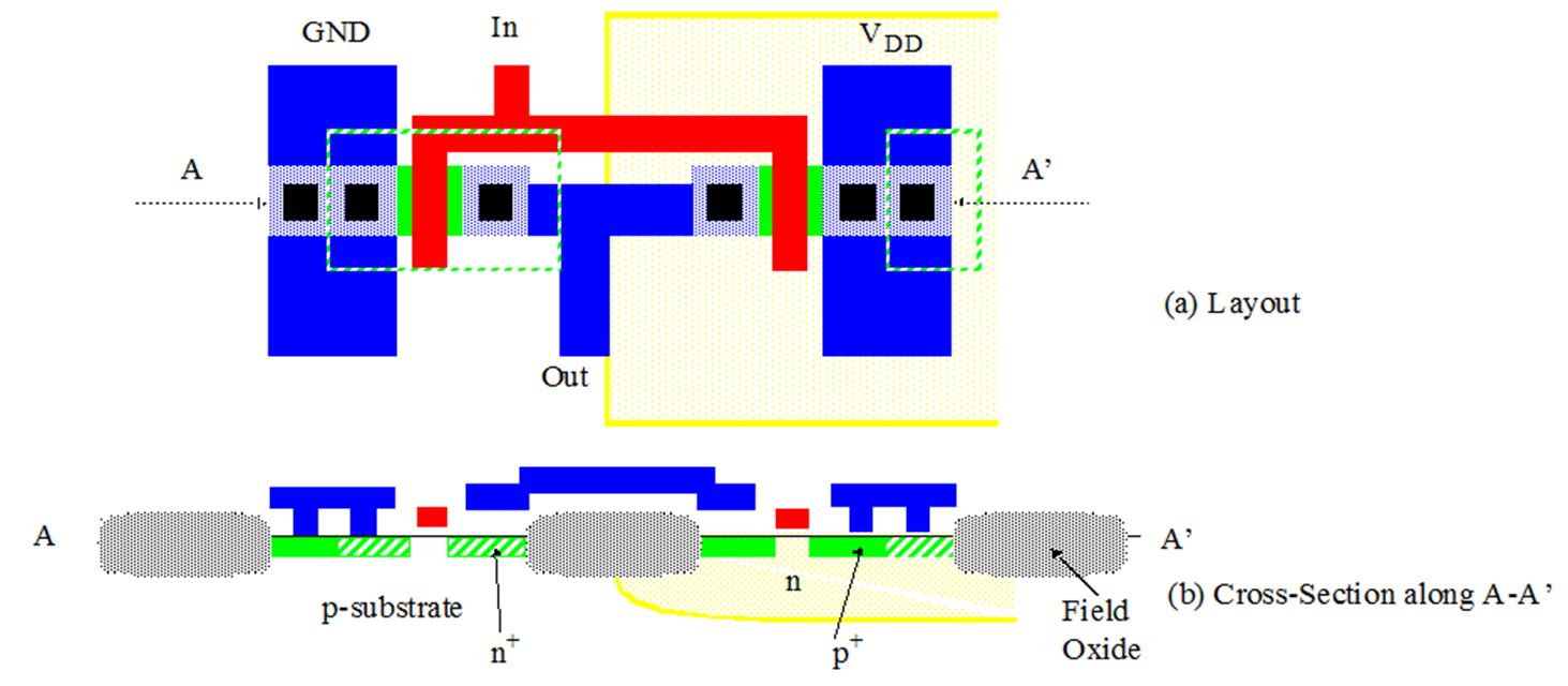
版图示例(Layout Example)
国际半导体技术路线图(The ITRS)
ITRS: International Technology Roadmap for Semiconductors
复杂性来源(The Complexity Sources)
随着技术节点的不断缩小,出现了新的可变性和可靠性问题:深亚微米 (DSM) 和纳米级设计中的新问题影响了IC的指标(metrics):
- 可靠性(Reliability)
- 成本(Cost)
- 性能(Performance)
- 功耗(Power consumption)
最主要复杂性来源(Principal complexity sources)
1.大的芯片面积(Large chip size)
-
密度Density: > (100/4) M Gate-Equivalent (2001); 1B Gate-Equivalent (2010, CMOS process at 22 nm node) ;
等效门:对应于一个双输入的与非门 Gate-equivalent: Corresponds to a two-input NAND gate (F = /(A·B); -
特征尺寸 λ : 大约是为制作在IC上的最小晶体管长度的一半 Feature size λ : Roughly half the length of the smallest transistor imprinted on an IC. For examples, λ = 0.125 μm for 0.25 μm CMOSIC ML process (1997); λ = 0.09 μm for 0.18 μm CMOSIC ML process (1999).
2.可变性和可靠性(Variability and reliability)
Variability (intrinsic)
- 随机掺杂波动Random doping fluctuation (RDF):表现出掺杂不均匀。
- 线边缘粗糙度Line edge roughness:表现出实际制作出来的互连线不是像画的版图那么直,而是坑坑洼洼的。
- 栅氧厚度的变化Tox variations and so on.
Reliability:
器件层面Device
- Vt variations: short-channel effects on Vt (hot-carrier effect, DIBL), intrinsic variability on Vt;短沟道效应影响Vt(要和沟道长度调制效应区分开来)
- Velocity saturation -> IDS lowing due to mobility (μ) degradation;**速度饱和效应,**比我们定义的过驱动电压低就已经饱和了。
- Thin-oxide tunneling / breakdown -> JG(gate leakage current density) increasing薄氧化物隧穿
互连层面Interconnect
- RC延时
- 信号完整性Signal Integrity: 串扰(Crosstalk),电迁移(Electromigration),电压降(IR drop), 时钟错位(Clock misalignment).
3.功耗(Power dissipation)
- 动态功耗(开关和短路电流)
- 静态功耗(亚阈值sub-threshold和泄漏电流leakage currents)
4.异构性(Heterogeneity)
从逻辑设计的角度来看,复杂性源于两个主要来源:异构性;及大小。From the logic design points of view, complexity arises from two principal sources: (i) heterogeneity; and (ii) size.
异构性迫使系统设计人员在做出设计决策时考虑来自多个领域的信息。Heterogeneity forces systems designers to consider information from multiple domains when making design decision.
比如数模混合电路考虑它们的供电问题,会相互影响。
3. 解决办法
- 设计抽象Design abstraction:It deals the complexity issue with a hierarchical composition of models
- 形式化表示Formal representation:Unambiguous design representation, which leads to design automation which helps IC designers complete design synthesis, implementation, and verification efficiently明确的设计表示,实现设计自动化,帮助IC设计人员高效完成设计综合、实现和验证。
- 深入的设计技术和方法In-depth design techniques and approaches:
⚫ Redesign of the library due to technology change. 工艺改了我也要能设计
⚫ Creating an adequate model of a cell requires an in-depth understanding of the internal operation. 对模型内部的操作要熟悉
⚫ The library-based approach works fine when the design constraints (speed, cost or power) are not stringent.
⚫ The impact of the interconnect parasitics is bound to with the scaling of the technology 考虑互连寄生效应
4. 一些设计挑战
- Design capability: EDA tools development
- Design verification: Methods and tools
- Time to market
- SoC and IP (Intellectual Property: predefined module) reuse
- Talented persona shortage and cooperation
- IC engineering organization and administration
- Risk: heavy capital investment
Design Abstraction and Representation
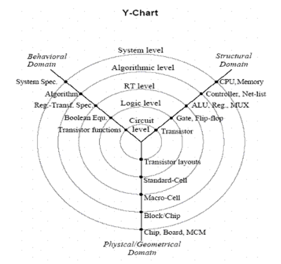
Y-Chart 表示法
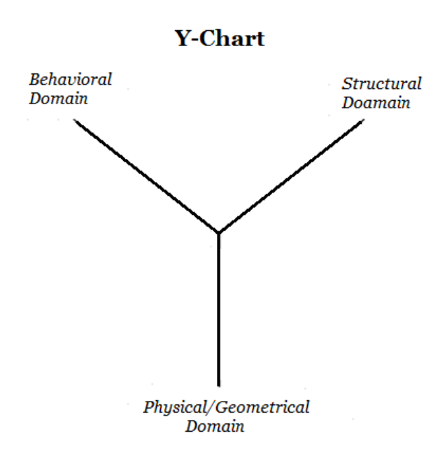
Y 型图表示是指在功能、结构和几何领域(function, structure and geometry)描述芯片的一种方式。
1. Behavioral (Functional) Representation (BR)
简单理解,把行为域描述看成一个布尔表达式。扩展点说,行为域描述可以看成一个黑盒,就是一个文本,数学形式或算法形式的描述
- Behavior represents a design as a black box and describes its outputs in terms of its inputs and time.
- The black-box behavior indicates no geometrical information or structural information. For example, an exclusive OR gate can be expressed in Boolean expression as XOR: X = A’B + AB’, where no geometrical or physical information is assumed, but, to some extent, structural information might be implied.
- Behavior takes the form of textual, mathematic or algorithmic description.
2. Structural Representation (SR)
简单理解,结构域描述可以看成一个逻辑门电路。扩展点说,结构域展示了有哪些元件和连线,是行为域和几何域的桥梁,但是它不包含物理信息。
- A black box is represented as a set of components and connections.
- It acts as a bridge between functional representation and geometrical representation.
- It may be generated by mapping functional representations onto a set of components and interconnections under a number of constraints in design space (typical axes in design space: area, speed, cost).
- No physical information is contained – parameters, such as size and position.
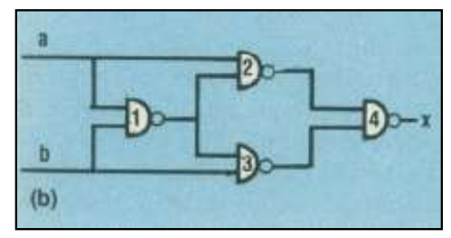
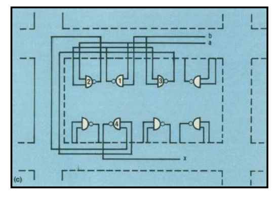
Structural representation of a Boolean expression
3. Geometrical Representation (GR)
简单理解,几何域可以看成物理版图。扩展点说,几何域包含了器件的尺寸,位置,端口和连线,扩散区,金属层,掩模版信息,是设计抽象的最底层。
- It specifies size (height and width), the position of each component, each port and connection on the silicon substrate or board.
- Geometrical shapes represent regions of diffusion, polysilicon, and metal on the silicon surface, etc…
- It includes mask information in layout file. This file is used to make masks of ICs.
- It is the lowest level of design abstraction.
Geometrical representation of a Boolean expression
行为描述的子类型(Sub-Types of Behavioral Descriptions)
- 算法描述Algorithmic description:It is a behavioral description in which the procedure defining the I/O response is not meant to imply any particular physical implementation. The description is often conducted through the algorithmic path of the component.比如算法框图,算法流程图等等
- 数据流描述Dataflow description:It is also a behavioral description in which the data dependencies in the description match those in the real implementation.比如verilog中的赋值语句就是一种数据流描述。
硬件描述语言
各种硬件描述语言就不赘述,就提一下它的优点。
硬件描述语言的优点
- 建模Modeling the design (formal representation),
- 综合和仿真验证Synthesis and verification (simulation), and
- 设计文档化Documenting a design.
一个可用的HDL至少应该得到综合器和仿真器的支持。 任何 HDL 的关键点都是对硬件模块的延迟和并发性进行建模的机制。
Y-Chart-Based Structured Design Concept
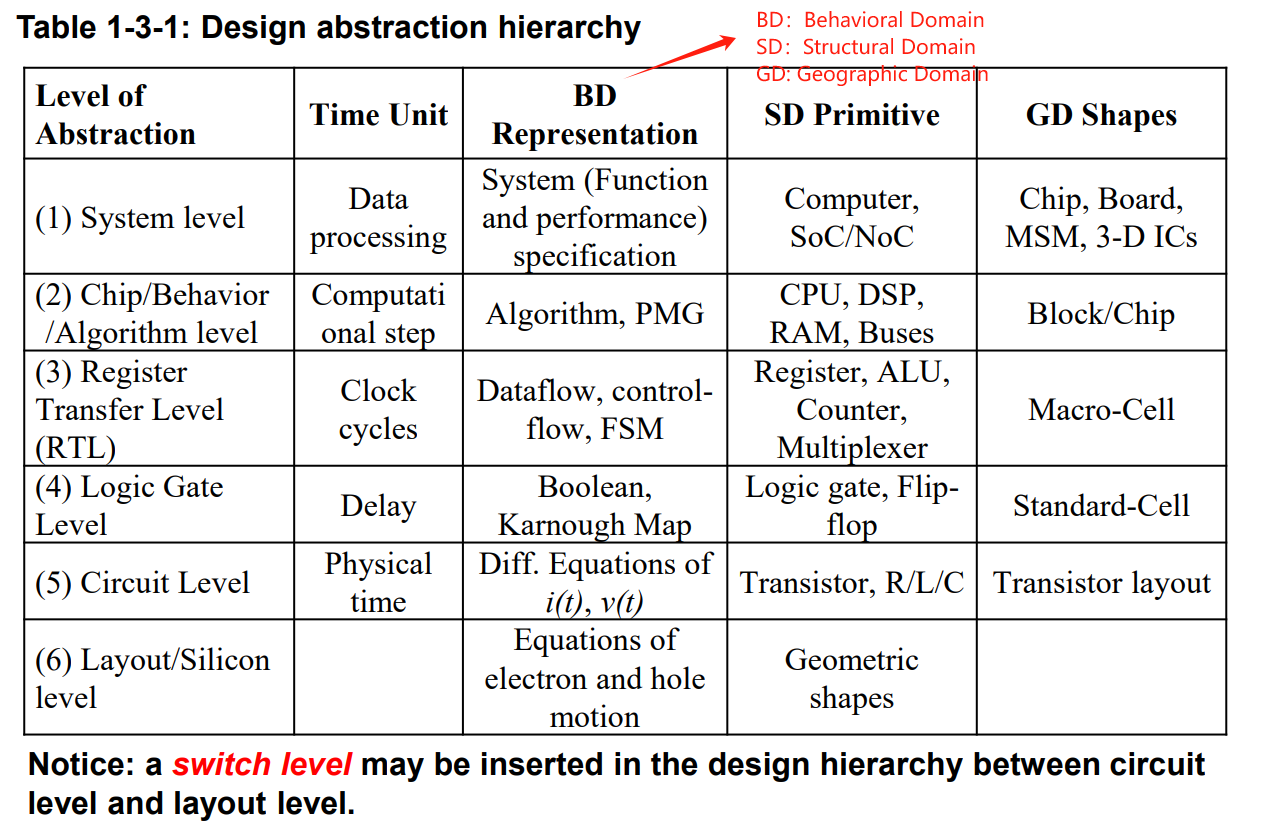
抽象层次
1. 基本定义
◆ Behavioral domain: A domain in which a component is described by defining its input / output response.
◆ Structural domain: A domain in which a component is described in terms of an interconnection of more primitive components.
◆ Physical domain: A domain in which a component is described by geometric shapes.
◆ 抽象层次结构Abstraction hierarchy: A set of interrelated representation levels that allow a system to be represented in varying amounts of detail.是指将硬件系统分为不同的层次,每个层次都有自己的功能和接口,而不用关心其他层次的细节。这样可以简化硬件设计的复杂度,提高硬件的可移植性和可维护性。
◆ 计算步骤Computational step: Data processing time (one or more clock cycles) between two successive input/output events, or two synchronous points. 两个连续输入事件间的数据处理时间,举个例子,CPU连续发出的两条指令之间的时间间隔。
2. 设计分层(Design Hierarchy)
设计与实现(Design and Implementation)
1. 设计活动(Design Activities)
- Design: A series of transformations from one representation of a system to another until a representation that can be fabricated exists.从系统的一种表示到另一种表示的一系列转换,直到存在可以制造的表示。
- Synthesis: The process of transforming one representation in the design abstraction hierarchy into another representation. (Synthesis = Translation + Optimization).将设计抽象层次结构中的一种表示形式转换为另一种表示形式的过程。
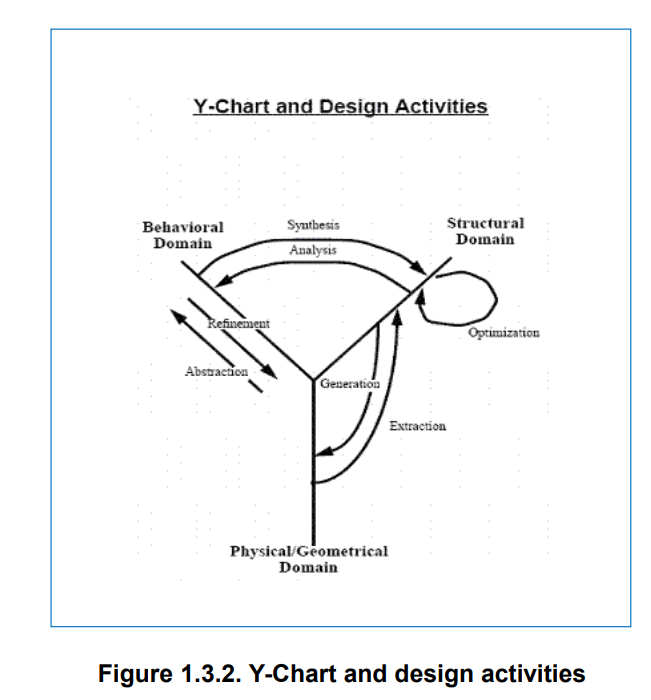
2. 设计和实现的关系(Relationship between Design and Implementation)
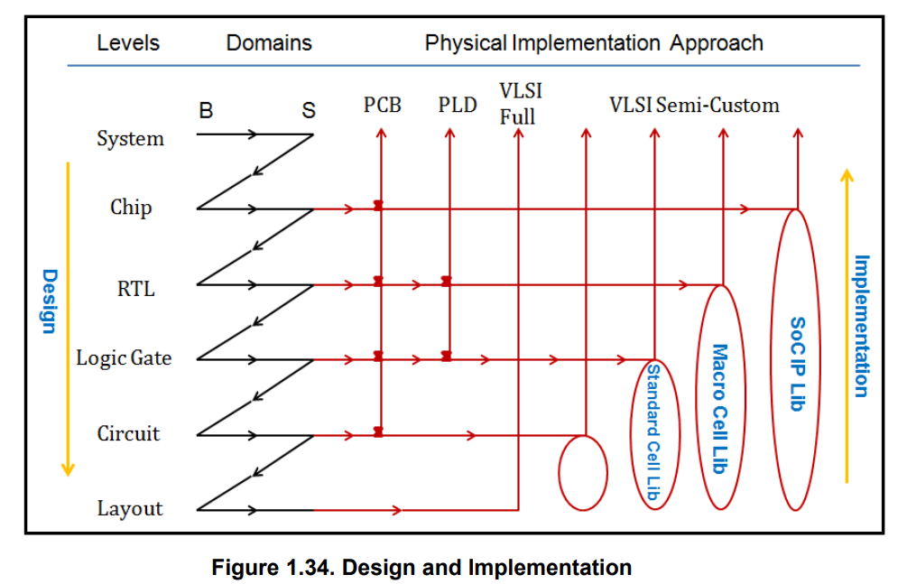
**硬件设计中的implementation指的是将综合后的门级网表转化为实际的版图的过程,也就是布局布线。**布局布线是一个优化的过程,需要在面积、速度、功耗等方面做出权衡。布局布线的结果会影响硬件的性能和可靠性。
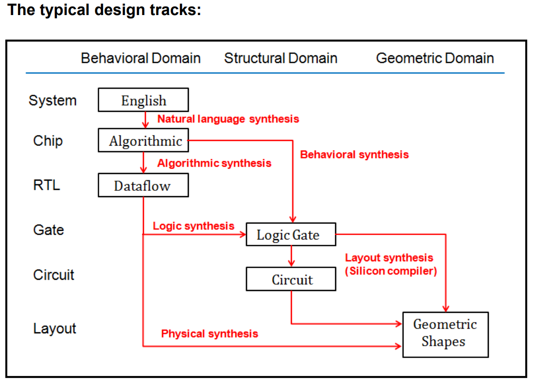
3.综合和设计周期(Synthesis and Design Cycle)
Design cycle: A series of synthesis steps.
The common synthesis steps include:
(1) Natural language synthesis: transformation from one form of design represented by one natural language (English, for example) to an algorithmic representation.从一种自然语言(例如英语)表示的一种设计形式转变为算法表示。
(2) System-level synthesis: mapping a task-level specification onto a heterogeneous hardware / software architecture.将任务级规范映射到异构硬件/软件架构上。
(3) Algorithmic synthesis (behavioral synthesis): translation from an algorithmic representation to a dataflow representation (or to a gate-level representation).从算法表示转换为数据流表示(或门级表示)。
(4) Logic synthesis: translation from a dataflow representation to a structural logic gate representation.从数据流表示到结构逻辑门表示的转换。
(5) Layout synthesis: translation from logic gate representation to layout representation.从逻辑门表示到布局表示的转换。
(6) Physical synthesis: creating a properly place-and-routed circuit from RTL code.** 从RTL代码创建正确的布局布线电路,相当于跳过了逻辑门级表示,直接从数据流到了版图**
IP 和 Y-Chart 表示
IP的概念
IP refers to the Intellectual Property (predefined module).
IP Cores
-
Each abstraction level needs a database of components on this level.
-
Each component in the database has three models representing three different axes in Y-Chart:
• Behavior or function (called Model of Computation, MoC), (Soft IP core)
• Structure of components from the low level of abstraction, (Hard IP core)
• Physical layout or implementation of the structure (Fixed IP core)
数字电路设计中,软核、硬核、固核是指不同程度的IP核(Intellectual Property Core)的交付方式。IP核是一种预先设计好的电路模块,可以用于ASIC、ASSP和PLD等芯片设计中。¹ -
软核(Soft IP Core)是由硬件描述语言(如Verilog或VHDL)设计的代码,没有经过综合和版图设计,因此具有高度的灵活性和可移植性,但也有一定的设计风险。
-
硬核(Hard IP Core)是经过验证的版图文件,已经完成了物理后端设计,可以直接用于生产,因此具有高度的可靠性和稳定性,但也有低度的灵活性和可移植性。
-
固核(Firm IP Core)是介于软核和硬核之间的一种交付方式,它是经过综合的网表文件,已经完成了部分的布局布线,但还可以通过编译器进行优化处理,因此具有一定的灵活性和可靠性。
简单理解,软核就是RTL代码,固核就是RTL综合成的网表,硬核就是根据网表画出来的版图


 302
302


 被折叠的 条评论
为什么被折叠?
被折叠的 条评论
为什么被折叠?
 到【灌水乐园】发言


