


 本文详细介绍了Xilinx UltraScale系列的SYSMON模块,包括其功能、ADC特性、采样模式、操作模式、接口以及状态和控制寄存器。通过仿真测试,展示了SYSMON在连续采样模式下的工作情况,涉及温度、片内电压和模拟输入通道的监测,并提供了温度转换计算示例。此外,还提到了与7系列XADC的区别以及相关配置参数的设定。
ultrascasle 系列片内监测模块叫SYSMON,7系列片内监测模块叫XADC。最近针对ultrascale系列的SYSMON和7系列的XADC做了相关调研、仿真、上板测试,这里先记录下SYSMON相关基础知识点和仿真结果。
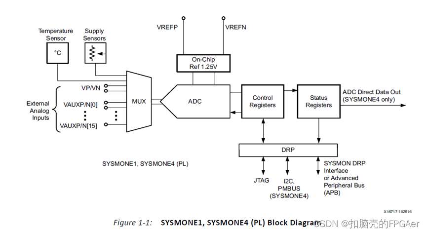
1、The SYSMON includes an analog-to-digital converter (ADC) as well as on-chip sensors that can be used to sample external voltages and monitor on-die operating conditions, such as temperature and supply voltage levels. SYSMON可以监测FPGA片内温度、片内供电电压,同时也可用于接入模拟信号,当做ADC使用。
2、The ADC supports differential sampling of unipolar and bipolar analog input signals and provides a wide range of operating modes to convert up to 17 external analog input channels.
3、Status registers store the ADC's sampled data, which can be accessed:
• Directly through the dynamic reconfiguration port (DRP) ports
• Through an external JTAG interface
• Through an I2C interface
• Through the power management bus (PMBus) for UltraScale+ devices
• Through the advanced peripheral bus (APB) for Zynq UltraScale+ MPSoC devices
4、The SYSMON interface can be simplified to drive a series of alarm ports based onuser-defined operating conditions, such as die temperature levels or power supply thresholds.
5、Block diagram:
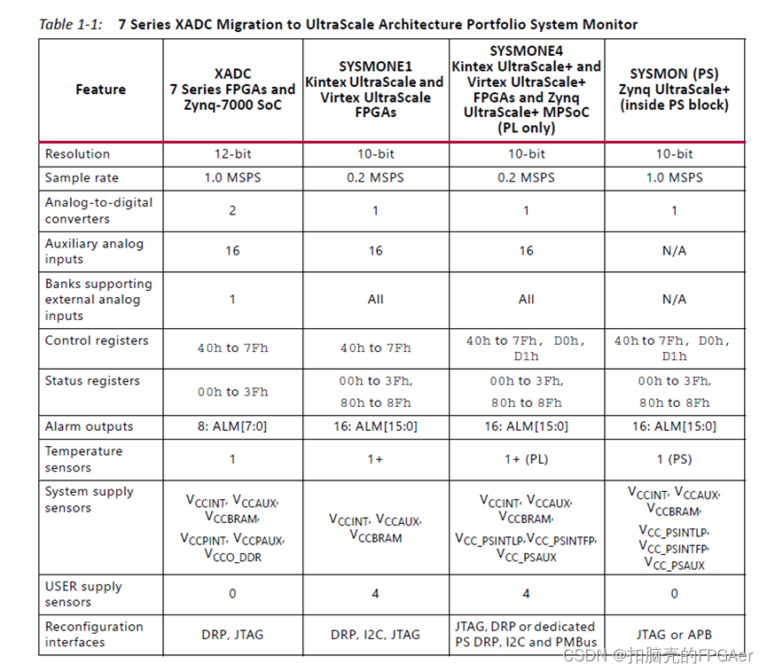
6、7 series XADC primitive and UltraScale SYSMON primitives:
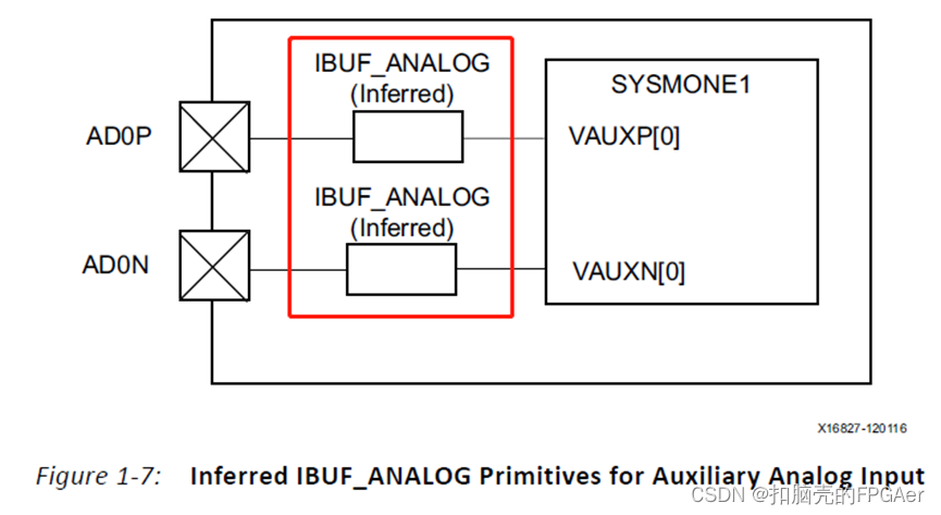
7、模拟输入至16对auxiliary analog inputs端口,vivado在编译时会自动添加原语IBUF_ANALOG,如下图所示:
8、 片上传感器的模拟数据无极性,外部模拟输入通道的模拟数据可以为有极性和无极性。
9、ADC输出的10位数据在状态寄存器(16位)的高10位,低6位用于提高精度(均值或滤波)。
10、SYSMON相关状态寄存器和控制寄存器地址范围:
SYSMON1
Status Registers (read only) 00h~3Fh 80h~FFh
Control Registers(read and write) 40h~7Fh
SYSMON4
Status Registers (read only) 00h~3Fh 80h~CFh
Control Registers(read and write) 40h~7fh
11、SYSMON重要应用点:
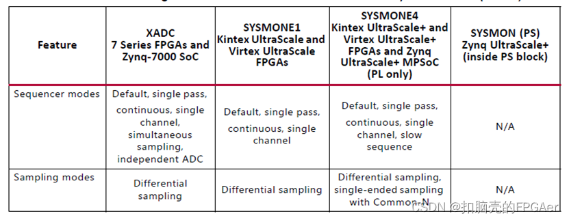
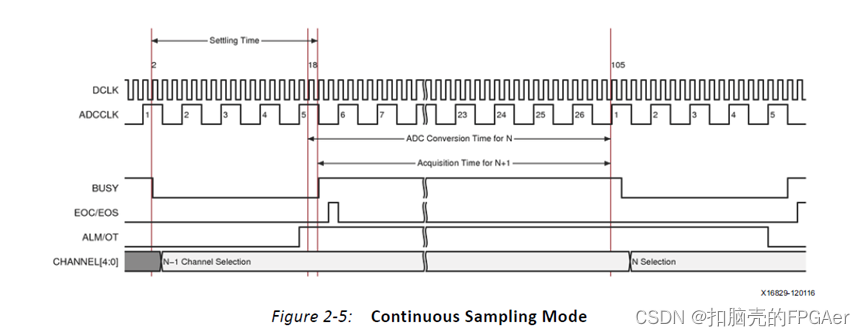
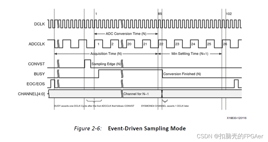
(1)Sampling Mode
Continuous sampling mode:
Event-Driven sampling mode:
(2)Operating Mode
Single Channel Mode
Automatic Channel Sequencer
Sequencer Modes :
1)Default Mode
2)Single Pass Mode
3)Continuous Sequence Mode(Slow Sequence – SYSMONE4)
4)Single Channel Mode(Sequencer off)
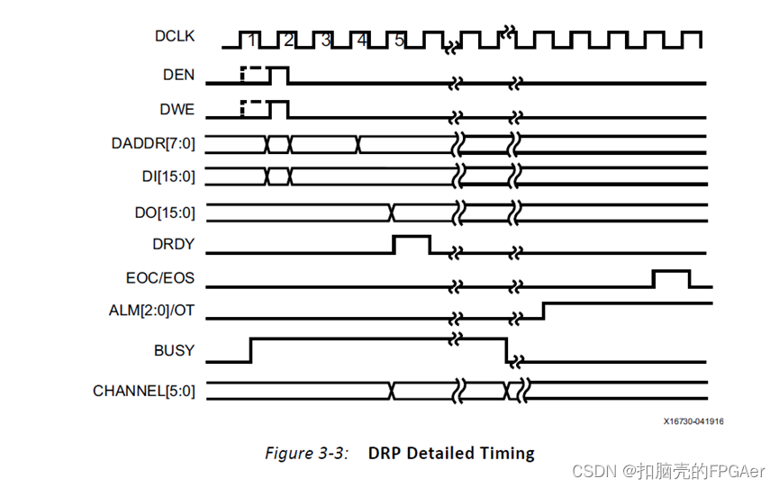
(3)Register interface
DRP Timing
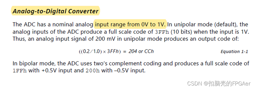
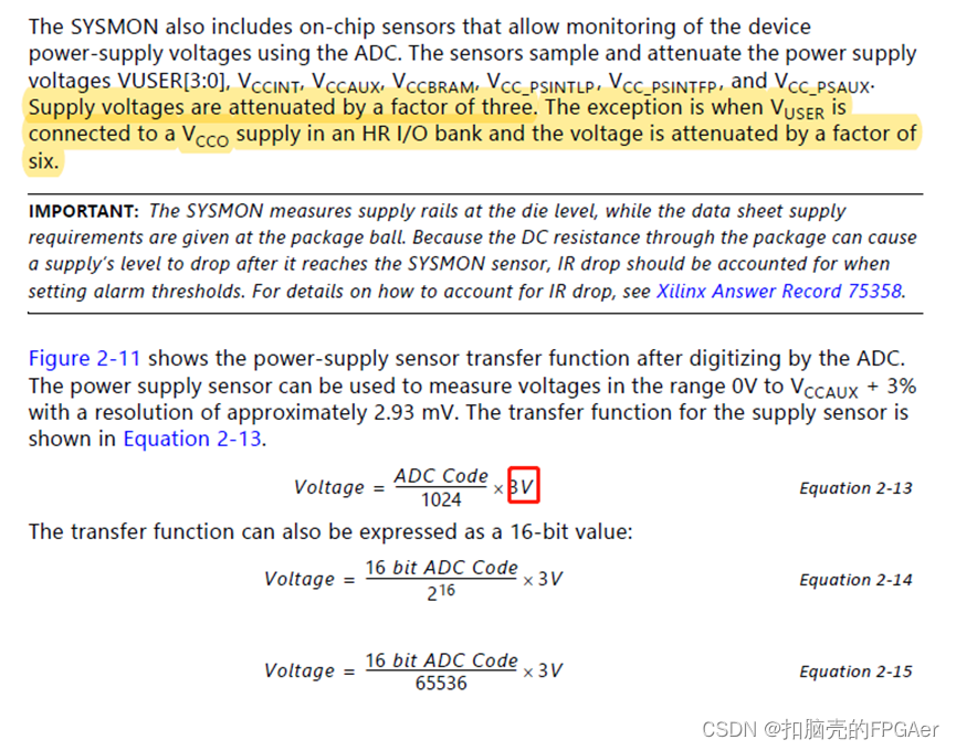
12、ADC参考电压1V
13、POWER AND USER SUPPLY sensor参考电压3V
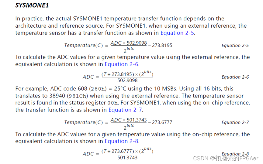
14、温度传感器
根据硬件上Vrefp和Vrefn是上拉(external reference)还是下拉(on-chip reference),去选择对应的计算公式。由于本次测试硬件上是下拉,所以选择使用了SYSMONE1的on-chip reference对应的计算公式。
仿真中给出的temp为10位(截取了16位数据的高10位),以0x262为例进行温度换算,(610 * 501.3743 / 1024) - 273.6777 = 24.99℃
15、功能仿真
针对SYSMON1进行了功能仿真, 在continuous采样模式下,ADC采样率为0.2MSPS,共计26个ADCCLK周期,可以计算出ADCCLK的频率最高位5.2MHz,ADCCLK可以通过DCLK进行比例关系设置,本次仿真设置DCLK为50MHz外部输入,ADCCLK为5MHz。
仿真测试了温度Temp、片内电压VCCINT、外部模拟输入通道aux 0~3
SYSMONE1 #(
// INIT_40 - INIT_44: SYSMON configuration registers
.INIT_40 (16'h9000 ), //Continuous Sampling Mode(26 ADCCLK cycles)
.INIT_41 (16'h2FDC ), //Continuous Sequence Mode, Enable ALM[0] / OT, Enable calibration
// .INIT_41 (16'h2FDD ), //Continuous Sequence Mode, Enable ALM[0], Enable calibration
.INIT_42 (16'h0A00 ), //ADCCLK = DCLK / 10 50MHz / 10 = 5MHz
.INIT_43 (16'h0000 ),
// .INIT_44 (16'h0000 ), //SYSMONE4 only
// .INIT_45 (16'h0000 ), //not use Analog Bus Register
// INIT_46 - INIT_4F: Sequence Registers
.INIT_46 (16'h0001 ), //SEQCHSEL0 - enable USER0 (channel select)
.INIT_47 (16'h0000 ), //SEQAVG0 disable (Averaging) , is use, 40h AVG1 and AVG2 can select the number of averaging
// .INIT_48 (16'h4701 ), //SEQCHSEL1 - enable Temp, VCCINT, VCCAUX, VCCBRAM, and calibration
.INIT_48 (16'h0301 ), //SEQCHSEL1 - enable Temp, VCCINT, calibration
.INIT_49 (16'h000F ), //SEQCHSEL2 - enable aux analog channels 0 - 3
.INIT_4A (16'h0000 ), //SEQAVG1 disable (Averaging)
.INIT_4B (16'h0000 ), //SEQAVG2 disable (Averaging)
.INIT_4C (16'h0000 ), //SEQINMODE0 - unipolar analog input for Vp and Vn
.INIT_4D (16'h0000 ), //SEQINMODE1 - unipolar analog input for AUX[15:0]
.INIT_4E (16'h0000 ), //SEQACQ0 - acquisition time (4 + 22 ADCCLK) for Vp and Vn
.INIT_4F (16'h0000 ), //SEQACQ1 - acquisition time (4 + 22 ADCCLK) for AUX[15:0]
// INIT_50 - INIT_5F: Alarm Limit Registers
.INIT_50 (16'hB723 ), //Temperature upper 85℃
.INIT_51 (16'h0000 ),
.INIT_52 (16'h0000 ),
.INIT_53 (16'hCB93 ), //OT upper 125℃
// .INIT_53 (16'h0000 ), //OT upper 125℃
.INIT_54 (16'hAA5F ), //Temperature lower 60℃
.INIT_55 (16'h0000 ),
.INIT_56 (16'h0000 ),
.INIT_57 (16'hAF7B ), //OT lower 70℃
// .INIT_57 (16'h0000 ), //OT lower 70℃
.INIT_58 (16'h0000 ),
.INIT_59 (16'h0000 ),
.INIT_5A (16'h0000 ),
.INIT_5B (16'h0000 ),
.INIT_5C (16'h0000 ),
.INIT_5D (16'h0000 ),
.INIT_5E (16'h0000 ),
.INIT_5F (16'h0000 ),
// INIT_60 - INIT_6F: User Supply Alarms
.INIT_60 (16'h0000 ),
.INIT_61 (16'h0000 ),
.INIT_62 (16'h0000 ),
.INIT_63 (16'h0000 ),
.INIT_64 (16'h0000 ),
.INIT_65 (16'h0000 ),
.INIT_66 (16'h0000 ),
.INIT_67 (16'h0000 ),
.INIT_68 (16'h0000 ),
.INIT_69 (16'h0000 ),
.INIT_6A (16'h0000 ),
.INIT_6B (16'h0000 ),
.INIT_6C (16'h0000 ),
.INIT_6D (16'h0000 ),
.INIT_6E (16'h0000 ),
.INIT_6F (16'h0000 ),
// Programmable Inversion Attributes: Specifies the use of the built-in programmable inversion on
// specific pins
.IS_CONVSTCLK_INVERTED (1'b0 ), // Optional inversion for CONVSTCLK, 0-1
.IS_DCLK_INVERTED (1'b0 ), // Optional inversion for DCLK, 0-1
// Simulation attributes: Set for proper simulation behavior
.SIM_MONITOR_FILE ("E:/project/sysmon/sysmon_test_1/sysmon_top.sim/design.txt"), // Analog simulation data file name
// User Voltage Monitor: SYSMON User voltage monitor
.SYSMON_VUSER0_BANK (66 ), // Specify IO Bank for User0
.SYSMON_VUSER0_MONITOR ("VCCO" ), // Specify Voltage for User0
.SYSMON_VUSER1_BANK (0 ), // Specify IO Bank for User1
.SYSMON_VUSER1_MONITOR ("NONE" ), // Specify Voltage for User1
.SYSMON_VUSER2_BANK (0 ), // Specify IO Bank for User2
.SYSMON_VUSER2_MONITOR ("NONE" ), // Specify Voltage for User2
.SYSMON_VUSER3_MONITOR ("NONE" ) // Specify Voltage for User3
)
SYSMONE1_inst (
// ALARMS outputs: ALM, OT
.ALM (w_alm ), // 16-bit output: Output alarm for temp, Vccint, Vccaux and Vccbram
.OT (w_ot ), // 1-bit output: Over-Temperature alarm
// Dynamic Reconfiguration Port (DRP) outputs: Dynamic Reconfiguration Ports
.DO (w_do ), // 16-bit output: DRP output data bus
.DRDY (w_drdy ), // 1-bit output: DRP data ready
// I2C Interface outputs: Ports used with the I2C DRP interface
.I2C_SCLK_TS ( ), // 1-bit output: I2C_SCLK output port
.I2C_SDA_TS ( ), // 1-bit output: I2C_SDA_TS output port
// STATUS outputs: SYSMON status ports
.BUSY (w_busy ), // 1-bit output: System Monitor busy output
.CHANNEL (w_channel ), // 6-bit output: Channel selection outputs
.EOC (w_eoc ), // 1-bit output: End of Conversion
.EOS (w_eos ), // 1-bit output: End of Sequence
.JTAGBUSY ( ), // 1-bit output: JTAG DRP transaction in progress output
.JTAGLOCKED ( ), // 1-bit output: JTAG requested DRP port lock
.JTAGMODIFIED ( ), // 1-bit output: JTAG Write to the DRP has occurred
.MUXADDR ( ), // 5-bit output: External MUX channel decode
// Auxiliary Analog-Input Pairs inputs: VAUXP[15:0], VAUXN[15:0]
.VAUXN (i_vauxn ), // 16-bit input: N-side auxiliary analog input
.VAUXP (i_vauxp ), // 16-bit input: P-side auxiliary analog input
// CONTROL and CLOCK inputs: Reset, conversion start and clock inputs
.CONVST (1'b0 ), // 1-bit input: Convert start input
.CONVSTCLK (1'b0 ), // 1-bit input: Convert start input
.RESET (w_rst ), // 1-bit input: Active-High reset
// Dedicated Analog Input Pair inputs: VP/VN
.VN (1'b0 ), // 1-bit input: N-side analog input
.VP (1'b0 ), // 1-bit input: P-side analog input
// Dynamic Reconfiguration Port (DRP) inputs: Dynamic Reconfiguration Ports
.DADDR (w_daddr ), // 8-bit input: DRP address bus
.DCLK (w_dclk ), // 1-bit input: DRP clock
.DEN (w_den ), // 1-bit input: DRP enable signal
.DI (w_di ), // 16-bit input: DRP input data bus
.DWE (w_dwe ), // 1-bit input: DRP write enable
// I2C Interface inputs: Ports used with the I2C DRP interface
.I2C_SCLK (1'b0 ), // 1-bit input: I2C_SCLK input port
.I2C_SDA (1'b0 ) // 1-bit input: I2C_SDA input port
);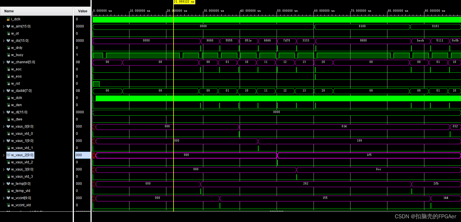
依次循环输出temp/vccint/vaux0/vaux1/vaux2/vaux3


 759
759

 被折叠的 条评论
为什么被折叠?
被折叠的 条评论
为什么被折叠?
 到【灌水乐园】发言


