


本文内容整理自西安交通大学软件学院李晨老师的课件,仅供学习使用,请勿转载
计算机组成原理系列笔记汇总:计算机组成原理笔记及思维导图汇总附复习建议_Qlz的博客-CSDN博客
文章目录
文章目录
本章思维导图
Semiconductor Memory
Organization
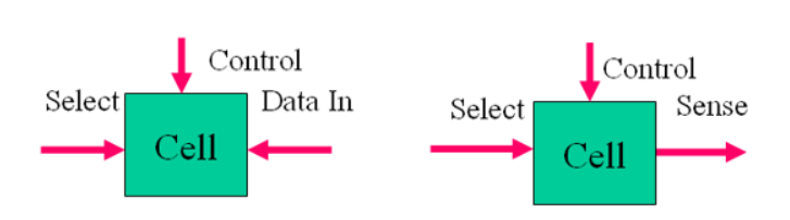
- Basic element of semi. memory is cell,which stores a digital bit;
- Cell Properties:
- Two states:1 or 0
- Can be set by write operation( at least once )
- Sensed by read operation
- Cell writing & Reading operation Fig.
RAM
RAM (random-access memory): access data by address
- Misnamed as all semiconductor memory is random access
- Read/Write: time is the same
- Volatile(易失性): DC supplies
- Temporary storage
- Static or dynamic
Dynamic RAM
- 数据存储在电容器中,充电为1,放电为0
- Charges leak:2ms duration
- Need refreshing even when powered
- Simpler construction
- Smaller per bit
- Less expensive and low power consumption
- Need refresh circuits
- Slower
- Main memory,由于其相比比较便宜,因此比较适合作为主存
- Essentially analogue
- Level of charge determines value
Dynamic RAM Structure
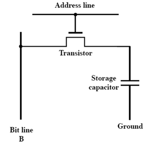
DRAM Operation
- 通过地址线选到该位时晶体管打开,使得电容与数据线直接相连
- Write
- 首先将数据放入bit line
- High for 1 low for 0
- 接着根据地址线选择合适的位
- 使电容充电或者放电
- 首先将数据放入bit line
- Read
- 选中地址线
- 晶体管打开
- 根据电容释放到位线上的电容连接到一个传感放大器上
- Compares with reference value to determine 0 or 1
- 电容器必须充电恢复
- 选中地址线
Static RAM
- 数据存储在寄存器门电路(flip-flop logic gate)中
- No refreshing needed when powered
- More complex construction
- Larger per bit: 6 MOS (Metal-oxide semiconductor)
- More expensive
- Does not need refresh circuits
- Faster
- Cache,因为速度比较快,所以比较适合做cache
- Digital
- Uses flip-flops
Stating RAM Structure
不懂
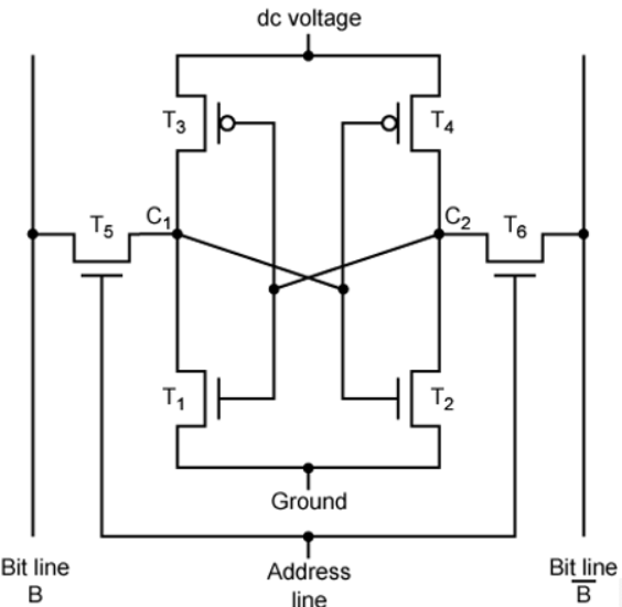
Static RAM Operation
- Transistor arrangement gives stable logic state
- State 1
- C1 high, C2 low
- T1 T4 off, T2 T3 on
- State 0
- C2 high, C1 low
- T2 T3 off, T1 T4 on
- Address line transistors T5 T6 is switch
- Write – apply value to B & compliment to B
- Read – value is on line B
SRAM v DRAM
- Both volatile 都是易失的
- Power needed to preserve data
- Dynamic cell
- Simpler to build, smaller
- More dense
- Less expensive
- Needs refresh
- Larger memory units
- Static
- Faster
- Cache
ROM
Read Only Memory
- Permanent storage 永久存储
- Read-only, can not be written
- Data wired into the chip while making
- A MOS means “1”, no MOS means “0”
- When a bit is error, the whole chip is useless
- Applications:
- Microprogramming
- Library subroutines
- Systems programs (BIOS)
- Function tables
PROM
programmable ROM
- Original chip produced, it can be written into only once by “programming”
- Special Equipment is required to program
- Writing process is performed electronically by: supplier or customer
- Fuse(保险丝) fired means 0, otherwise, means 1
- Flexibility & convenience
Read “mostly” Memory
Read is more frequent than write, nonvolatile applications
- EPROM
- EEPROM
- Flash memory
Erasable Programmable ROM (EPROM)
- Read and write electronically
- Initializing chip in ultraviolet radiation(紫外线)
- 20 minutes to write, multiple updating
- expensive
Electronically EPROM (EEPROM)
- No need erasing prior contents,acting as disk
- Write is longer than read
- More expensive than EPROM
- Less dense
Flash Memory
- A type of semiconductor memory is used both for internal memory and external memory applications
- Price, function is between EPROM~EEPROM
- Erase by blocks, no needing erasing whole chip
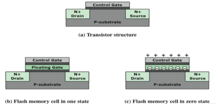
图看不太懂
Two distinctive types of flash memory
-
NOR
- The basic unit of access is a bit
- Provides high-speed random access
- Used for microcontrollers where the amount of program code is relatively small and a certain amount of application data does not vary
-
NAND
-
The basic unit is 16 or 32 bits
-
Reads and writes in small blocks
-
Does not provide a random-access external address bus so the data must be read on a block-wise basis
不提供随机访问的外部地址总线,因此必须按块读取数据
-
-
NAND memory is better suited for external memory, such as USB flash drives, memory cards, and in what are known as solid-state disks (SSDs)
Summary for Semiconductor Memory

Module Organization
Chip Logic
- Packaged chip
- Array of Cells
- Word or cell
- Key design issue:
- Word length:data bits read or written each
- Organization modes:
- Physical arrangement of the cells in the array is the same as the logical arrangement
- e.g.: 16 M b i t = 1 M × 16 b i t , o r 2 M × 8 b i t 16Mbit=1M\times 16bit, \ or \ 2M \times8bit 16Mbit=1M×16bit, or 2M×8bit
- Cell/word
- e.g.: 16 M b i t = 16 M × 1 b i t 16Mbit=16M \times1bit 16Mbit=16M×1bit
- Others
- e.g.: 16 M b i t = 4 M × 4 b i t 16Mbit=4M \times4bit 16Mbit=4M×4bit
- Physical arrangement of the cells in the array is the same as the logical arrangement
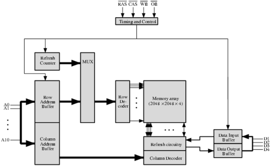
Typical 16M-bit DRAM (4M x 4)
该图注意事项:
- 由于这该芯片是DRAM,因此需要一个更新电路(refresh circunitry)
- 对于数据存放来说,将数据组织为矩阵形式,根据行号和列号来查找,对于memory array块来说,是四块芯片叠加在一起,根据行号列号同时查找四个芯片上对应位置的数据,并将其放入Data Output Buffer中
- 对于取出的数据还需要放入Data Input Buffer中,同时更新电路需要根据其中的值将对应位置的数据进行重新加载
- 信号说明
- R A S ‾ \overline{RAS} RAS:行选择信号,表示现在输入的数据(A0-A10)是行号还是列号
- C A S ‾ \overline{CAS} CAS:列选择信号,表示现在输入的数据(A0-A10)是行号还是列号
- W E ‾ \overline{WE} WE:读写信号
- O E ‾ \overline{OE} OE:输出使能信号
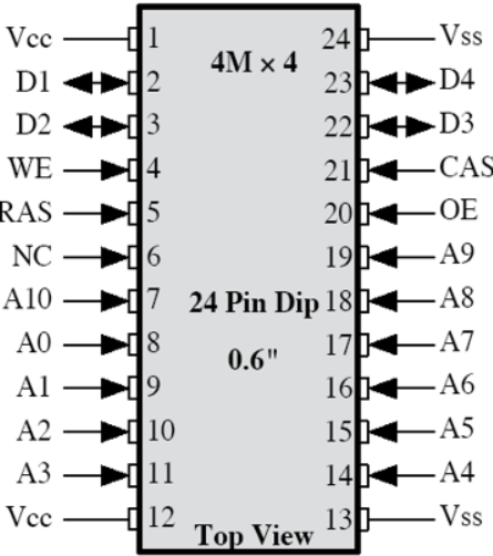
一般芯片引脚说明
- Typical structure of 16M DRAM: 4 x 2048 x 2048 array, 4bits/word
- Multiplexing 11 address lines, address bits= 22, Save on pins;
- RAS: Row address selection
- CAS: Column address selection
- WE: Write enable
- OE: Output enable
- Refreshing row by row
- No operations while refreshing
- Refresh before reading or writing
Extension
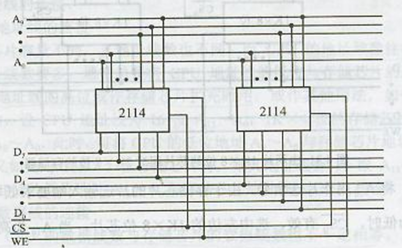
word length extension
1 K × 4 → 1 K × 8 1K\times4 \rightarrow 1K\times8 1K×4→1K×8
对于字长度的扩展,首先需要计算出需要多少个已有芯片才可以组成需求的字节大小,然后将地址线接到所有芯片上,同时将读写使能信号与片选信号也都接在一起,只需要按照特定的规定将芯片连接到数据线的不同位即可
2114含义:4表示直接长度为4,第二个1表示大小为1k
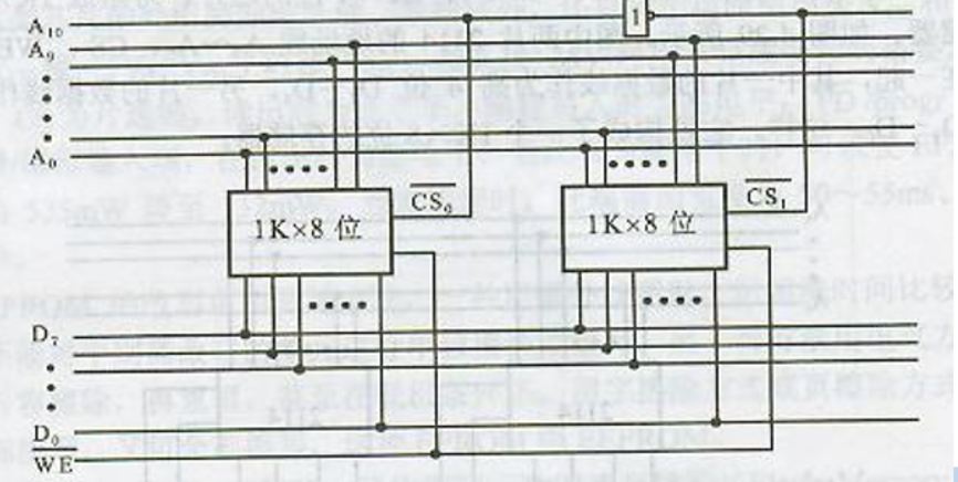
word number extension
1 K × 8 → 2 K × 8 1K\times8 \rightarrow 2K\times8 1K×8→2K×8
对于字地址的扩展需要从地址中选择几位作为片选信号(一般都是地址高位),对于扩大两倍的直接使用非门即可,对于扩大两倍以上的则需要使用译码器进行片选
word length and number extension
1 K × 4 → 2 K × 8 1K\times4 \rightarrow 2K\times8 1K×4→2K×8
两者都扩大的一般先扩大字长度,然后扩大地址长度

Connection of CPU and Memory
- Connection of address lines
- CPU的地址线一般比内存的地址线要大,因为还要连接I/O
- 一般将内存的地址线连在CPU的低位地址线上
- CPU地址线的高位一般用来做片选
- Connection of data lines
- CPU的数据线必须等于内存的数据位,必要时,放大芯片位
- Connection command line
- Read/write lines are directly connected to that of memory
- CS is connected to MREQ and high address bits of CPU
- Logic circuit may be used, such as decoder
- Correctly select types of chip and number
- ROM used for system area
- RAM used for user area
例子
Error Correction
- Hard Failure
- Permanent defect
- Soft Error
- Random, non-destructive
- No permanent damage to memory
- Detected using Hamming error correcting code
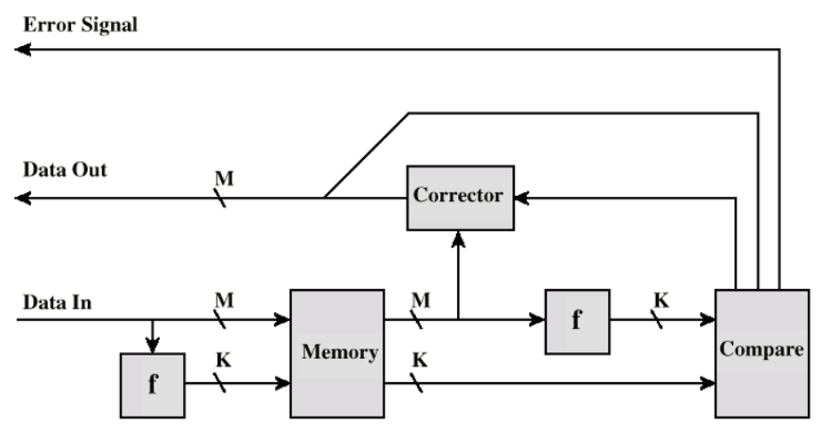
Error Correcting Code Function
海明码,缺二查一,较一般的字缺少两位用来存储标志位,可以检查出来并且改正一位的错误
Advanced DRAM Organization
- Basic DRAM keeps same since first RAM chips
- Enhanced(增强的) DRAM
- Contains small SRAM as well
- SRAM holds last line read
- Cache DRAM
- Larger SRAM component
- Used as cache or serial buffer
Synchronous DRAM (SDRAM)
比较重要
- Access is synchronized with an external clock
- 地址呈现给RAM
- RAM查找数据(对于传统的DRAM来说,CPU此时处于等待状态)
- 因为SDRAM是按照系统时钟传输数据,因此CPU知道什么时候数据被准备好了
- 因此CPU不需要等待,它可以做一些其他事,因为有锁存机制(latch)
- 突发模式(Burst mode)允许SDRAM设置数据流,并在块中发射它
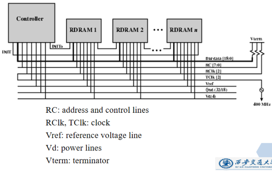
RAMBUS
- Adopted by Intel for Pentium & Itanium
- Main competitor to SDRAM
- Vertical package – all pins on one side
- Data exchange over 28 wires < 12cm long
- Bus addresses up to 320 RDRAM chips at 1.6Gbps
- Asynchronous block protocol
- 480ns access time
- Then 1.6 Gbps
DDR SDRAM
比较重要
- SDRAM can only send data once per clock
- Double-data-rate SDRAM can send data twice per clock cycle
- Rising edge and falling edge
- DDR4
- DDR V4
- Introduced in 2011
- enlarging the prefetch buffer (small cache)
Vocabulary
- MO(magneto-optical disk):磁光盘
- Data-In/Sense Terminal:数据输入/输出端
- RAS(row address select):行地址选择
- CAS(column address select):列地址选择
- Module:模块
- Flash memory: 快闪存储器
- Hard failure: 硬件故障
- Soft error: 软件故障
- Error correction :差错校验/纠错
- Hamming error-correction code:海明差错校验码
- Parity bit:校验位
- Syndrome word:错误字
- Reliability:可靠性
- Latch:锁存器
- Volatile memory: 易失性存储器
Key Points
- Differences between SRAM and DRAM?
- Comparing EPROM and Flash memory!
- What is SDRAM? what applications need it?
- Parallel DRAM techniques


 5834
5834


 被折叠的 条评论
为什么被折叠?
被折叠的 条评论
为什么被折叠?
 到【灌水乐园】发言


