


目录
一、简介
(1)
(2)
二、Spec
(1)Function descripton
(2)Interface description
| Signal Name | Width | Type Direction | Description |
|---|---|---|---|
| clk | 1 | input | System clk signal, 50Mhz |
| rst | 1 | input | System reset signal,negedge |
(3)Block Diagram
(4)Design detil
- List item
(5)Timing
三、Design and Verification
- RTL
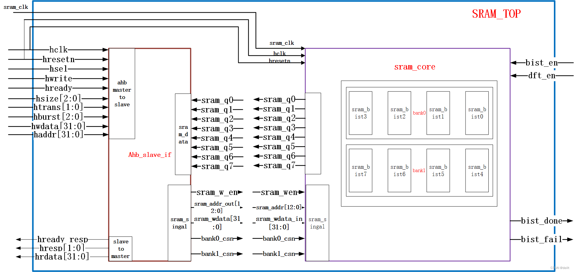
SRAM_TOP
/*----------------------------------------------------------
Filename			    :	sram_top
Author					:	deilt
Description				:	sram 可以同时提供读写功能且存取时间区别不大.
Called by				:
Revision History		:	10/06/2022
                            Revison 1.0
Email					:	cjdeilt@qq.com
Company:Deilt Technology.INC
Copyright(c) 1999, Deilt Technology Inc, All right reserved
--------------------------------------------------------------*/
module sramc_top(
  //input signals
  input wire			hclk,
  input wire			sram_clk,
  input wire    		hresetn,
  input wire    		hsel,
  input wire   	 	    hwrite,
  input wire			hready,
  input wire [2:0]  	hsize ,
  input wire [2:0]  	hburst,
  input wire [1:0]  	htrans,
  input wire [31:0] 	hwdata,
  input wire [31:0] 	haddr,
  //Signals for BIST and DFT test mode
  //When signal"dft_en" or "bist_en" is high, sram controller enters into test mode.
  input wire            dft_en,
  input wire            bist_en,

  //output signals
  output wire         	hready_resp,
  output wire [1:0]   	hresp,
  output wire [31:0] 	hrdata,
  //When "bist_done" is high, it shows BIST test is over.
  output wire        	bist_done,
  //"bist_fail" shows the results of each sram funtions.There are 8 srams in this controller.
  output wire [7:0]     bist_fail
  );

  //Select one of the two sram blocks according to the value of sram_csn
  wire [3:0] bank0_csn;
  wire [3:0] bank1_csn;

  //Sram read or write signals: When it is high, read sram; low, writesram.
  wire  sram_w_en;

  //Each of 8 srams is 8kx8, the depth is 2^13, so the sram's address width is 13 bits.
  wire [12:0] sram_addr;

  //AHB bus data write into srams
  wire [31:0] sram_wdata;

  //sram data output data which selected and read by AHB bus
  wire [7:0] sram_q0;
  wire [7:0] sram_q1;
  wire [7:0] sram_q2;
  wire [7:0] sram_q3;
  wire [7:0] sram_q4;
  wire [7:0] sram_q5;
  wire [7:0] sram_q6;
  wire [7:0] sram_q7;


  // Instance the two modules:
  // ahb_slave_if.v and sram_core.v

  ahb_slave_if  ahb_slave_if_u(
    //-----------------------------------------
    // AHB input signals into sram controller
    //-----------------------------------------
    .hclk     (hclk),
    .hresetn  (hresetn),
    .hsel     (hsel),
    .hwrite   (hwrite),
    .hready   (hready),
    .hsize    (hsize),
    .htrans   (htrans),
    .hburst   (hburst),
    .hwdata   (hwdata),
    .haddr    (haddr),

    //-----------------------------------------
    //8 sram blcoks data output into ahb slave
    //interface
    //-----------------------------------------
    .sram_q0   (sram_q0),
    .sram_q1   (sram_q1),
    .sram_q2   (sram_q2),
    .sram_q3   (sram_q3),
    .sram_q4   (sram_q4),
    .sram_q5   (sram_q5),
    .sram_q6   (sram_q6),
    .sram_q7   (sram_q7),

    //---------------------------------------------
    //AHB slave(sram controller) output signals
    //---------------------------------------------
    .hready_resp  (hready_resp),
    .hresp        (hresp),
    .hrdata       (hrdata),

    //---------------------------------------------
    //sram control signals and sram address
    //---------------------------------------------
	.sram_w_en    (sram_w_en),
	.sram_addr_out(sram_addr),
     //data write into sram
	.sram_wdata   (sram_wdata),
    //choose the corresponding sram in a bank, active low
    .bank0_csn    (bank0_csn),
    .bank1_csn    (bank1_csn)
	);


  sram_core  sram_core_u(
    //AHB bus signals
    .hclk        (hclk    ),
    .sram_clk    (sram_clk),
	.hresetn     (hresetn ),

    //-------------------------------------------
    //sram control singals from ahb_slave_if.v
    //-------------------------------------------
	.sram_addr    (sram_addr ),
	.sram_wdata_in(sram_wdata),
	.sram_wen     (sram_w_en ),
	.bank0_csn    (bank0_csn ),
	.bank1_csn    (bank1_csn ),

    //test mode enable signals
	.bist_en      (bist_en   ),
	.dft_en       (dft_en    ),

    //-------------------------------------------
    //8 srams data output into AHB bus
    //-------------------------------------------
    .sram_q0    (sram_q0),
    .sram_q1    (sram_q1),
    .sram_q2    (sram_q2),
    .sram_q3    (sram_q3),
    .sram_q4    (sram_q4),
    .sram_q5    (sram_q5),
    .sram_q6    (sram_q6),
    .sram_q7    (sram_q7),

    //test results output when in test mode
    .bist_done  (bist_done),
    .bist_fail  (bist_fail)
    );

endmodule
ahb_slave_if
/*----------------------------------------------------------
Filename			    :	ahb_slave_if
Author					:	deilt
Description				:
Called by				:
Revision History		:	10/6/2022
                            Revison 1.0
Email					:	cjdeilt@qq.com
Company:Deilt Technology.INC
Copyright(c) 1999, Deilt Technology Inc, All right reserved
--------------------------------------------------------------*/
module
#(
    parameter       HADDR_WIDTH     =   32  ,
    parameter       SRAM_ADDR_WIDTH =   13  ,
    parameter       DATA_WIDTH      =   32  ,
    parameter       SRAM_Q_WIDTH    =   8

)
(
    //-------------------------------------------------
    //AHB port
    //reset and clock
    input                           hclk            ,
    input                           hresetn         ,
    //select
    input                           hsel            ,
    //address and control
    input                           hready          ,
    input   [HADDR_WIDTH-1:0]       haddr           ,
    input                           hwrite          ,
    input   [1:0]                   htrans          ,
    input   [2:0]                   hsize           ,
    input   [2:0]                   hburst          ,
    //data
    input   [DATA_WIDTH-1:0]        hwdata          ,
    output  [DATA_WIDTH-1:0]        hrdata          ,
    //ahb_slave response
    output                          hready_resp     ,
    output  [1:0]                   hresp           ,
    //-------------------------------------------------
    //sram
    input   [SRAM_Q_WIDTH-1:0]      sram_q0         ,
    input   [SRAM_Q_WIDTH-1:0]      sram_q1         ,
    input   [SRAM_Q_WIDTH-1:0]      sram_q2         ,
    input   [SRAM_Q_WIDTH-1:0]      sram_q3         ,
    input   [SRAM_Q_WIDTH-1:0]      sram_q4         ,
    input   [SRAM_Q_WIDTH-1:0]      sram_q5         ,
    input   [SRAM_Q_WIDTH-1:0]      sram_q6         ,
    input   [SRAM_Q_WIDTH-1:0]      sram_q7         ,
    //-------------------------------------------------
    //sram control signal
    output                          sram_w_en       ,   //0:write  1:read
    output  [SRAM_ADDR_WIDTH-1:0]   sram_addr_out   ,   //13bit 8K
    output  [DATA_WIDTH-1:0]        sram_wdata      ,   //write sram data 32bit
    output  [3:0]                   bank0_csn       ,   //low is enable
    output  [3:0]                   bank1_csn
);

    //htrans[1:0] , in this project ,only in NONSEQ and SEQ can normal operation
    localparam  IDLE    =   2'b00   ,
                BUSY    =   2'b00   ,
                NONSEQ  =   2'b10   ,
                SEQ     =   2'b11   ;

    //ahb slave input signals
    reg     [HADDR_WIDTH-1:0]       haddr           ;
    reg                             hwrite          ;
    reg     [1:0]                   htrans          ;
    reg     [2:0]                   hsize           ;
    reg     [2:0]                   hburst          ;

    //buf signal
    reg     [HADDR_WIDTH-1:0]       haddr_buf       ;
    reg                             hwrite_buf      ;
    reg     [1:0]                   htrans_buf      ;
    reg     [2:0]                   hsize_buf       ;
    reg     [2:0]                   hburst_buf      ;

    //
    wire    [15:0]                  sram_addr       ;   //haddr---->sram_addr
    wire    [1:0]                   haddr_sramqx_sel;   //Used to select which SRAM to operate and reduce power consumption

    wire                            bank_sel        ;
    wire                            sram_csn_en     ;

    wire    [3:0]                   bank0_csn       ;
    wire    [3:0]                   bank1_csn       ;
    wire    [1:0]                   sram_sel        ;
    wire    [1:0]                   hsize_sel       ;
    reg     [3:0]                   sram_csn        ;

    //read or write judgment
    wire                            sram_read       ;
    wire                            sram_write      ;

    //singal cycle transport,hready_resp = 1
    //hrep = okay
    assign  hready_resp   =   1'b1  ;   //singal cycle
    assign  hresp         =   2'b00 ;   // resp is OK

    //generate sram address
    //SRAM 8k*8总寻址64K 0x0--0xffff
    assign  sram_addr           =   haddr[15:0]             ;   //the sram_addr[15] is the minimun of the next bank
    assign  sram_addr_out       =   sram_addr[14:2]         ;   //13bit

    assign  haddr_sramqx_sel    =   haddr[1:0]              ;

    //ahb input delay(buf)
    always @(posedge hclk or negedge hresetn) begin
        if(!hresetn)begin
            hwrite_buf  <=    1'b0  ;
            hsize_buf   <=    3'b0  ;
            htrans_buf  <=    2'b0  ;
            hburst_buf  <=    3'b0  ;
            haddr_buf   <=    {HADDR_WIDTH{1'b0}}   ;
        end
        else if(hsel && hready)begin        //hsel要片选,否则信号一直在翻转,可能会功能错误,并且功耗大
            hwrite_buf  <=  hwrite  ;       //写SRAM时,把控制信号寄存。因为写操作时,要把地址打一拍,和数据对齐
            hsize_buf   <=  hsize   ;
            htrans_buf  <=  htrans  ;
            hburst_buf  <=  hburst  ;       //可以不用
            haddr_buf   <=  haddr   ;
        end
        else begin
            hwrite_buf  <=    1'b0  ;
            hsize_buf   <=    3'b0  ;
            htrans_buf  <=    2'b0  ;
            hburst_buf  <=    3'b0  ;
            haddr_buf   <=    {HADDR_WIDTH{1'b0}}   ;
    end
    end

    //write enable && read enable
    assign  sram_read     =   (htrans == NONSEQ || htrans ==  SEQ) && hwrite  ;
    assign  sram_write    =   (htrans == NONSEQ || htrans ==  SEQ) && !hwrite ;
    assign  sram_w_en     =   !sram_write_en   ;

    //sram bank csn
    //低32K bank0 高32K bank1
    //sram_csn_en is mean sram is work
    //sram_csn mean 4bit ,which sram is work
    assign  sram_csn_en   =   sram_read  ||  sram_write   ;
    assign  bank_sel      =   (sram_csn_en  &&  sram_addr[15] == 1'b0) ? 1'b1 : 1'b0    ;

    //sram 0-7 csn ,determine the hsize[2:0] 8,16,32bits
    //low is valid
    //in bank0_csn  ,which sram is work
    assign bank0_csn    =   (bank_sel == 1'b1)  ? sram_csn : 4'b1111 ;
    assign bank1_csn    =   (bank_sel == 1'b0 ) ? sram_csn : 4'b1111 ;

    assign  hsize_sel   =   hsize_buf[1:0]  ;   //how many bits
    assign  sram_sel    =   sram_addr[1:0]  ;   //which sram is work 00--1 2 3 4

    always @(*)begin
        if(hsize_sel == 2'b10)    //32bit
            sram_csn    =   4'b0    ;
        else if(hsize_sel == 2'b01)begin  //16bit
            if(sram_sel[1] == 1'b1)
                sram_csn    =   4'b0011 ;
            else
                sram_csn    =   4'b1100 ;
        end
        else if(hsizi_sel == 2'b00)begin  //8bit
            case(sram_sel)
                2'b00 : sram_csn  =  4'b1110 ;
                2'b01 : sram_csn  =  4'b1101 ;
                2'b10 : sram_csn  =  4'b1011 ;
                2'b11 : sram_csn  =  4'b0111 ;
                default:sram_csn  =  4'b1111 ;
            endcase
        end
        else
            sram_csn    =   4'b1111 ;
    end

    //write operation
    assign  sram_wdata = hwdata ;
    //read opretion
    // If bank_sel = 1'b1, bank0 sleceted, or bank1 selected.
    assign hrdata   =   (bank_sel == 1) ? {sram_q3,sram_q2,sram_q1,sram_q0} : {sram_q7,sram_q6,sram_q5,sram_q4};

endmodule
sram_core
/*----------------------------------------------------------
Filename			    :	sram_core
Author					: 	deilt
Description				:	同步、单端口SRAM , 例化了8片sram
Called by				:
Revision History		:	10/06/2022
                            Revison 1.0
Email					:	cjdeilt@qq.com
Company:Deilt Technology.INC
Copyright(c) 1999, Deilt Technology Inc, All right reserved
--------------------------------------------------------------*/
module sram_core(
  //input signals
  input			    hclk,
  input			    sram_clk,
  input			    hresetn,

  input			    sram_wen,        // =1 读sram; =0,写sram.8个一起读或者一起写
  input	[12:0]	sram_addr,
  input	[31:0]	sram_wdata_in,   //data write into sram when "sram_wen_in" active low
  input	[3:0]	  bank0_csn,       //两个bank,每个bank有四个片选
  input	[3:0]	  bank1_csn,
  input			    bist_en,         //BIST test mode
  input	    	  dft_en,          //DFT test mode

  //output signals
  output [7:0]	sram_q0,
  output [7:0]	sram_q1,
  output [7:0]	sram_q2,
  output [7:0]	sram_q3,
  output [7:0]	sram_q4,
  output [7:0]	sram_q5,
  output [7:0]	sram_q6,
  output [7:0]	sram_q7,

  output			  bist_done,  //When "bist_done" is high, it shows BIST test is over.
  output [7:0]  bist_fail   //"bist_fail" shows the results of each sram funtions.
  );

  //Every sram bist's work state and results output.
  wire bist_done0;
  wire bist_fail0;
  wire bist_done1;
  wire bist_fail1;
  wire bist_done2;
  wire bist_fail2;
  wire bist_done3;
  wire bist_fail3;
  wire bist_done4;
  wire bist_fail4;
  wire bist_done5;
  wire bist_fail5;
  wire bist_done6;
  wire bist_fail6;
  wire bist_done7;
  wire bist_fail7;

  wire bank0_bistdone;
  wire bank1_bistdone;

  wire [3:0] bank0_bistfail;
  wire [3:0] bank1_bistfail;

  //bist finishing state of bank0
  assign bank0_bistdone = (bist_done3 && bist_done2) && (bist_done1 && bist_done0);

  //bist results of bank0
  assign bank0_bistfail = {bist_fail3,bist_fail2,bist_fail1,bist_fail0};

  //bist finishing state of bank1
  assign bank1_bistdone = (bist_done7 && bist_done6) && (bist_done5 && bist_done4);

  //bist results of bank1
  assign bank1_bistfail = {bist_fail7,bist_fail6,bist_fail5,bist_fail4};

  //--------------------------------------------------------------------------
  //the 8 srams results of BIST test and the finishing state
  //--------------------------------------------------------------------------
  assign bist_done = bank0_bistdone && bank1_bistdone;
  assign bist_fail = {bank1_bistfail,bank0_bistfail} ;

  //-------------------------------------------------------------------------
  //Instance 8 srams and each provides with BIST and DFT functions.
  //Bank0 comprises of sram0~sram3, and bank1 comprises of sram4~sram7.
  //In each bank, the sram control signals broadcast to each sram, and data
  //written per byte into each sram in little-endian style.
  //-------------------------------------------------------------------------
  //bank0 bank1读写使能以及地址都完全相同,写入的数据也相同

  sram_bist u_sram_bist0(
                        .hclk             (hclk),
                        .sram_clk         (sram_clk),
                        .sram_rst_n       (hresetn),
                        .sram_csn_in      (bank0_csn[0]),
                        .sram_wen_in      (sram_wen),
                        .sram_addr_in     (sram_addr),
                        .sram_wdata_in    (sram_wdata_in[7:0]),
                        .bist_en          (bist_en),
		                .dft_en           (dft_en),

                        .sram_data_out    (sram_q0),
                        .bist_done        (bist_done0),
                        .bist_fail        (bist_fail0)
                       );

  sram_bist u_sram_bist1(
                        .hclk             (hclk),
                        .sram_clk         (sram_clk),
                        .sram_rst_n       (hresetn),
                        .sram_csn_in      (bank0_csn[1]),
                        .sram_wen_in      (sram_wen),
                        .sram_addr_in     (sram_addr),
                        .sram_wdata_in    (sram_wdata_in[15:8]),
                        .bist_en          (bist_en),
		                .dft_en           (dft_en),

                        .sram_data_out    (sram_q1),
                        .bist_done        (bist_done1),
                        .bist_fail        (bist_fail1)
                       );

  sram_bist u_sram_bist2(
                        .hclk             (hclk),
                        .sram_clk         (sram_clk),
                        .sram_rst_n       (hresetn),
                        .sram_csn_in      (bank0_csn[2]),
                        .sram_wen_in      (sram_wen),
                        .sram_addr_in     (sram_addr),
                        .sram_wdata_in    (sram_wdata_in[23:16]),
                        .bist_en          (bist_en),
		                .dft_en           (dft_en),

                        .sram_data_out    (sram_q2),
                        .bist_done        (bist_done2),
                        .bist_fail        (bist_fail2)
                       );

  sram_bist u_sram_bist3(
                        .hclk             (hclk),
                        .sram_clk         (sram_clk),
                        .sram_rst_n       (hresetn),
                        .sram_csn_in      (bank0_csn[3]),
                        .sram_wen_in      (sram_wen),
                        .sram_addr_in     (sram_addr),
                        .sram_wdata_in    (sram_wdata_in[31:24]),
                        .bist_en          (bist_en),
		                .dft_en           (dft_en),

                        .sram_data_out    (sram_q3),
                        .bist_done        (bist_done3),
                        .bist_fail        (bist_fail3)
                       );

  sram_bist u_sram_bist4(
                        .hclk             (hclk),
                        .sram_clk         (sram_clk),
                        .sram_rst_n       (hresetn),
                        .sram_csn_in      (bank1_csn[0]),
                        .sram_wen_in      (sram_wen),
                        .sram_addr_in     (sram_addr),
                        .sram_wdata_in    (sram_wdata_in[7:0]),
                        .bist_en          (bist_en),
		                .dft_en           (dft_en),

                        .sram_data_out    (sram_q4),
                        .bist_done        (bist_done4),
                        .bist_fail        (bist_fail4)
                       );

  sram_bist u_sram_bist5(
                        .hclk             (hclk),
                        .sram_clk         (sram_clk),
                        .sram_rst_n       (hresetn),
                        .sram_csn_in      (bank1_csn[1]),
                        .sram_wen_in      (sram_wen),
                        .sram_addr_in     (sram_addr),
                        .sram_wdata_in    (sram_wdata_in[15:8]),
                        .bist_en          (bist_en),
		                .dft_en           (dft_en),

                        .sram_data_out    (sram_q5),
                        .bist_done        (bist_done5),
                        .bist_fail        (bist_fail5)
                       );

  sram_bist u_sram_bist6(
                        .hclk             (hclk),
                        .sram_clk         (sram_clk),
                        .sram_rst_n       (hresetn),
                        .sram_csn_in      (bank1_csn[2]),
                        .sram_wen_in      (sram_wen),
                        .sram_addr_in     (sram_addr),
                        .sram_wdata_in    (sram_wdata_in[23:16]),
                        .bist_en          (bist_en),
		                .dft_en           (dft_en),

                        .sram_data_out    (sram_q6),
                        .bist_done        (bist_done6),
                        .bist_fail        (bist_fail6)
                       );

  sram_bist u_sram_bist7(
                        .hclk             (hclk),
                        .sram_clk         (sram_clk),
                        .sram_rst_n       (hresetn),
                        .sram_csn_in      (bank1_csn[3]),
                        .sram_wen_in      (sram_wen),
                        .sram_addr_in     (sram_addr),
                        .sram_wdata_in    (sram_wdata_in[31:24]),
                        .bist_en          (bist_en),
		                .dft_en           (dft_en),

                        .sram_data_out    (sram_q7),
                        .bist_done        (bist_done7),
                        .bist_fail        (bist_fail7)
                       );

endmodule
sram_bist
/*----------------------------------------------------------
Filename			      :	mbist_8kx8
Author					    :	deilt
Description				  :
Called by				    :
Revision History		:	10/10/2022
                      Revison 1.0
Email					      :	cjdeilt@qq.com
Company:Deilt Technology.INC
Copyright(c) 1999, Deilt Technology Inc, All right reserved
--------------------------------------------------------------*/
module sram_bist(
  //input signals
  input         hclk,
  input         sram_clk,
  input         sram_rst_n,
  input         sram_csn_in,   //chip select enable
  input         sram_wen_in,   //sram write or read enable; 0:write; 1:read
  input[12:0]   sram_addr_in,
  input[7:0 ]   sram_wdata_in,
  input         bist_en,       // MBIST mode
  input         dft_en,        // DFT mode

  //output signals
  output[7:0 ]  sram_data_out,
  output        bist_done,     // 1: test over
  output        bist_fail      // high: MBIST Fail
  );

  //----------------------------------------------------
  //Internal signals connected the sram with bist module
  //when "bist_en" active high.
  //----------------------------------------------------
  wire sram_csn;
  wire sram_wen;
  wire sram_oen;
  wire [12:0] sram_a;
  wire [7:0]  sram_d;
  wire [7:0]  data_out;

  //Sram output data when "dft_en" active high.
  wire [7:0] dft_data;
  reg [7:0]  dft_data_r;

  wire [12:0] sram_addr;
  wire [7:0]  sram_wdata;

  //clock for bist logic, when bist is not work, clock should be 0.
  wire bist_clk;

  genvar K;

  //block sram input when cs is diable for low power design
  assign sram_addr = sram_csn_in ? 0 : sram_addr_in;
  assign sram_wdata = sram_csn_in ? 0 : sram_wdata_in;

  //dft test result
  assign dft_data = (sram_d ^ sram_a[7:0]) ^ {sram_csn, sram_wen, sram_oen, sram_a[12:8]};

  always @(posedge hclk or negedge sram_rst_n) begin
    if(!sram_rst_n)
      dft_data_r <= 0;
    else if(dft_en)
      dft_data_r <= dft_data;
  end

  //sram data output
  assign sram_data_out = dft_en ? dft_data_r : data_out;
  // Note: Need to take place the mux using the special library cell
/*
  generate for(K = 0; K < 8; K = K+1 )
    begin :hold
    //BHDBWP7T holdQ (.Z(data_out[K]));
    end
  endgenerate
*/

  //clock for bist logic, when bist is not work, clock should be 0.
  // Note: Need to take place the mux using the special library cell
  // CKMUX2D2BWP7T U_bist_clk_mux (.I0(1'b0), .I1(hclk), .S(bist_en), .Z(bist_clk));
  assign bist_clk = bist_en ? hclk : 1'b0;

  // One sram with BIST and DFT function
  RA1SH u_RA1SH(
        .Q      (data_out),
        .CLK    (sram_clk),
        .CEN    (sram_csn),
        .WEN    (sram_wen),
        .A      (sram_a),
        .D      (sram_d),
        .OEN    (sram_oen)
       );

  mbist_8kx8 u_mbist_8kx8(
        .b_clk   (bist_clk),
        .b_rst_n (sram_rst_n),
        .b_te    (bist_en),
		     //--------------------------------------------------------
		     //All the input signals will be derectly connected to
		     //the sram input when in normal operation; and when in
		     //BIST TEST mode, there are some mux in BIST module
		     //selcting all sram input signals which generated by itself:
		     //sram controll signals, sram write data, etc.
		     //--------------------------------------------------------
         .addr_fun     (sram_addr),
         .wen_fun      (sram_wen_in),
         .cen_fun      (sram_csn_in),
         .oen_fun      (1'b0),
         .data_fun     (sram_wdata),

         .ram_read_out (sram_data_out),
         .data_test    (sram_d),
         .addr_test    (sram_a),
         .wen_test     (sram_wen),
         .cen_test     (sram_csn),
         .oen_test     (sram_oen),

         .b_done       (bist_done),
         .b_fail       (bist_fail)
       );

endmodule
mbist_8kx8
/*----------------------------------------------------------
Filename			      :	mbist_8kx8
Author					    :	deilt
Description				  :
Called by				    :
Revision History		:	10/10/2022
                            Revison 1.0
Email					:	cjdeilt@qq.com
Company:Deilt Technology.INC
Copyright(c) 1999, Deilt Technology Inc, All right reserved
--------------------------------------------------------------*/
module mbist_8kx8
#(parameter WE_WIDTH = 1,
  parameter ADDR_WIDTH = 13,
  parameter DATA_WIDTH = 8
 )
 (
  //input signals
  input                      b_clk,    // bist clock
  input                      b_rst_n,  // bist resetn
  input                      b_te,     // bist enable
  input [(ADDR_WIDTH-1):0]   addr_fun,
  input [(WE_WIDTH-1):0]     wen_fun,
	input                      cen_fun,
	input                      oen_fun,
	input [(DATA_WIDTH-1):0]   data_fun,
	input [(DATA_WIDTH-1):0]   ram_read_out,
  //output signals
	output [(ADDR_WIDTH-1):0]  addr_test, // address of test
	output [(WE_WIDTH-1):0]    wen_test,  // writing control of bist test mode
	output                     cen_test,  // chip enable control of bist test mode
	output                     oen_test,  // output enable control of bist test mode
  output [(DATA_WIDTH-1):0]  data_test, // data input of bist test mode
	output				             b_done,    // output state of bist test mode
                                        // When "bist_done" is high, it shows BIST test is over.

	output reg                 b_fail     // output result of sram function
                                        // When "bist_fail" is high, the sram function is wrong;
                                        // else, the sram function is right.
  );

  //----------------------------------------------------
  //Define 27 work states of BIST block for bist test
  //----------------------------------------------------
  `define IDEL1         5'b00000
  `define P1_WRITE0     5'b00001
  `define IDEL2         5'b00010
  `define P2_READ0      5'b00011
  `define P2_COMPARE0   5'b00100
  `define P2_WRITE1     5'b00101
  `define IDEL3         5'b00110
  `define P3_READ1      5'b00111
  `define P3_COMPARE1   5'b01000
  `define P3_WRITE0     5'b01001
  `define P3_READ0      5'b01010
  `define P3_COMPARE0   5'b01011
  `define P3_WRITE1     5'b01100
  `define IDEL4         5'b01101
  `define P4_READ1      5'b01110
  `define P4_COMPARE1   5'b01111
  `define P4_WRITE0     5'b10000
  `define IDEL5         5'b10001
  `define P5_READ0      5'b10010
  `define P5_COMPARE0   5'b10011
  `define P5_WRITE1     5'b10100
  `define P5_READ1      5'b10101
  `define P5_COMPARE1   5'b10110
  `define P5_WRITE0     5'b10111
  `define IDEL6         5'b11000
  `define P6_READ0      5'b11001
  `define P6_COMPARE0   5'b11010

  // sram address when in bist test mode
  reg [(ADDR_WIDTH-1):0] test_addr;

  // bist test end signal
  reg r_end;
  reg r_end_en;

  // sram address reset when in bist test mode.
  reg test_addr_rst;

  // sram read or write enable signal when in bist test mode
  reg [(WE_WIDTH-1):0] wen_test_inner;

  // bist start to work in IDLE
  reg rf_start;

  // compare the data read from sram with the data written into sram
  // enable signal
  reg check_en;

  // bist test data source select signal
  // "pattern_sel == 1'b0"-----> test_pattern =  32'b0;
  // "pattern_sel == 1'b1"-----> test_pattern =  32'b1;
  reg pattern_sel;
  wire [(DATA_WIDTH-1):0] test_pattern;
  reg [4:0] cstate, nstate;
  // 1 -- address is goign upward; 0 -- address is going downward
  reg up1_down0;
  // 1 -- address is stepping; 0 -- address remains
  reg count_en;

  //-----------------------------------------------------------------
  //     Combinatorial portion
  //-----------------------------------------------------------------
  assign b_done = r_end;
  assign test_pattern = (pattern_sel == 1'b0) ? {DATA_WIDTH{1'b0}} : {DATA_WIDTH{1'b1}};

  //--------------------------------------------------------------------
  // The output values of all the mux below will be changed based on the
  // sram whether in normal operation or in bist test mode.
  //---------------------------------------------------------------------
  assign data_test = (b_te == 1'b1) ? test_pattern   : data_fun;
  assign addr_test = (b_te == 1'b1) ? test_addr      : addr_fun;
  assign wen_test  = (b_te == 1'b1) ? wen_test_inner : wen_fun;
  assign cen_test  = (b_te == 1'b1) ? 1'b0           : cen_fun;
  assign oen_test  = (b_te == 1'b1) ? 1'b0           : oen_fun;

  //--------------------------------------------------------------------
  //    Sequential portion
  //--------------------------------------------------------------------

  //--------------------------------
  // Generate bist work end signal.
  //--------------------------------
  always @(posedge b_clk , negedge b_rst_n) begin
    if (b_rst_n == 1'b0)
       r_end<=1'b0;
    else if (r_end_en == 1'b1)
       r_end<= 1'b1;
       else
         r_end <= 1'b0;
  end
  //----------------------------------------------------
  //          Generate the sram test address.
  // "test_addr_rst " and "up1_down0" decide the mode of
  // variable the address(increment/decrement).
  //-----------------------------------------------------
  always @(posedge b_clk , negedge b_rst_n) begin
    if (b_rst_n == 1'b0)
       test_addr <= {ADDR_WIDTH{1'b0}};
    else if (b_te == 1'b1)
  	  if (test_addr_rst == 1'b1)
           if (up1_down0 == 1'b1)
          	  test_addr<=  {ADDR_WIDTH{1'b0}};
           else
              test_addr<=  {ADDR_WIDTH{1'b1}};
     	else
           if (count_en == 1'b1)
               if (up1_down0 == 1'b1)
          	      test_addr<=  test_addr + 1'b1;
               else
                  test_addr<=  test_addr - 1'b1;
  end

  always @(posedge b_clk , negedge b_rst_n)
    if (b_rst_n == 1'b0)
       b_fail<=1'b1;
    else begin
      //---------------------------------------------------------
      //  When in bist idle1 state, "b_fail" defualt value is "0".
      // --------------------------------------------------------
      if ((b_te == 1'b1) && (rf_start == 1'b1))
          b_fail<=  1'b0;

      //------------------------------------------------------------
      //  "b_fail" value is "1", when data read from sram is different
      // from the expected data wirtten into sram.
      //--------------------------------------------------------------
      if ((b_te == 1'b1) && (check_en == 1'b1) && !(test_pattern == ram_read_out))
          b_fail<=  1'b1;
     end

  //------------------------------------------------------------------------------
  //                    Bist test state machine
  //   write "0"(initial sram)                         test_address 0-->1fff
  //   read  "0"------> compare -------->write "1"     test_address 1fff-->0
  //   read  "1"------> compare -------->write "0"     test_address 0-->1fff
  //   write "1"------> read "1"-------->compare       test_address 1fff-->0
  //   write "0"------> read "0"-------->compare       test_address 0-->1fff
  //   write "1"------> read "1"-------->compare       test_address 1fff-->0
  //   write "0"------> read "0"-------->compare       test_address 0-->1fff
  //------------------------------------------------------------------------------
  always @(posedge b_clk , negedge b_rst_n) begin
    if (b_rst_n == 1'b0)
          cstate<=`IDEL1;
    else
          cstate<= nstate;
  end

  always @(cstate or b_te or r_end or test_addr) begin
    up1_down0     = 1'b1;
    count_en      = 1'b0;
    r_end_en      = 1'b0;
    pattern_sel   = 1'b0;
    test_addr_rst = 1'b0;
    rf_start      = 1'b0;
    check_en      = 1'b0;
    wen_test_inner = {WE_WIDTH{1'b1}};
    nstate        = cstate;
    case (cstate)
      `IDEL1 :
          begin
             test_addr_rst = 1'b1;
             if (b_te == 1'b1 && r_end == 1'b0) begin
                   nstate   = `P1_WRITE0;
                   rf_start = 1'b1;
             end
          end
      `P1_WRITE0 :   //initial sram from addr 0~1fff
          begin
    	    count_en       = 1'b1;
    	    wen_test_inner = {WE_WIDTH{1'b0}};
    	    pattern_sel    = 1'b0;
             if (test_addr == {ADDR_WIDTH{1'b1}} ) begin
                  nstate        = `IDEL2;
                  test_addr_rst = 1'b1;
    	            up1_down0     = 1'b0;
             end
          end
      `IDEL2 :
          begin
    	      pattern_sel   = 1'b0;
    	      up1_down0     = 1'b0;
            test_addr_rst = 1'b1;
            nstate        = `P2_READ0;
          end
      `P2_READ0 :
          begin
            nstate = `P2_COMPARE0;
          end
      `P2_COMPARE0 :  //compare all "0" data after read from addr 0~1fff
          begin
             pattern_sel = 1'b0;
    	       check_en    = 1'b1;
             nstate      = `P2_WRITE1;
          end
      `P2_WRITE1 :  //all "1" write test from addr 1fff~0
          begin
    	      up1_down0      = 1'b0;
    	      count_en       = 1'b1;
    	      wen_test_inner = {WE_WIDTH{1'b0}};
    	      pattern_sel    = 1'b1;
             if (test_addr == {ADDR_WIDTH{1'b0}}) begin
                  nstate        = `IDEL3;
                  test_addr_rst = 1'b1;
    	          up1_down0     = 1'b1;
             end
             else
                nstate        = `P2_READ0;
          end
      `IDEL3 :
          begin
             pattern_sel   = 1'b1;
             test_addr_rst = 1'b1;
             nstate        = `P3_READ1;
          end
      `P3_READ1 :
          begin
             nstate = `P3_COMPARE1;
          end
      `P3_COMPARE1 :  //compare all "1" data after read from addr 1fff~0
          begin
            pattern_sel = 1'b1;
            check_en    = 1'b1;
            nstate      = `P3_WRITE0;
          end
      `P3_WRITE0 :
          begin
             wen_test_inner = {WE_WIDTH{1'b0}};
             pattern_sel    = 1'b0;
             nstate         = `P3_READ0;
          end
      `P3_READ0 :
          begin
            nstate = `P3_COMPARE0;
          end
      `P3_COMPARE0 :
          begin
            pattern_sel = 1'b0;
            check_en    = 1'b1;
            nstate      = `P3_WRITE1;
          end
      `P3_WRITE1 :
          begin
             wen_test_inner = {WE_WIDTH{1'b0}};
             pattern_sel    = 1'b1;
             count_en       = 1'b1;
             if (test_addr == {ADDR_WIDTH{1'b1}}) begin
                  nstate        = `IDEL4;
                  test_addr_rst = 1'b1;
             end
             else
                nstate        = `P3_READ1;
          end
      `IDEL4 :   // read all data from addr 1fff~0 and compare with write data "1" every time
          begin
            pattern_sel   = 1'b1;
            test_addr_rst = 1'b1;
            nstate        = `P4_READ1;
          end
      `P4_READ1 :
          begin
            nstate = `P4_COMPARE1;
          end
      `P4_COMPARE1 :
          begin
            pattern_sel = 1'b1;
            check_en    = 1'b1;
            nstate      = `P4_WRITE0;
          end
      `P4_WRITE0 :
          begin
            wen_test_inner = {WE_WIDTH{1'b0}};
            pattern_sel    = 1'b0;
            count_en       = 1'b1;
             if (test_addr == {ADDR_WIDTH{1'b1}}) begin
                   nstate        = `IDEL5;
                   test_addr_rst = 1'b1;
             end
             else
                nstate        = `P4_READ1;
          end
      `IDEL5 :  // read all data from addr 1fff~0 and compare with write data "0" every time
          begin
             pattern_sel   = 1'b1;
             test_addr_rst = 1'b1;
             nstate        = `P5_READ0;
          end
      `P5_READ0 :
          begin
             nstate = `P5_COMPARE0;
          end
      `P5_COMPARE0 :
          begin
             pattern_sel=1'b0;
             check_en=1'b1;
             nstate = `P5_WRITE1;
          end
      `P5_WRITE1 :
          begin
             wen_test_inner = {WE_WIDTH{1'b0}};
             pattern_sel   = 1'b1;
             nstate = `P5_READ1;
          end
      `P5_READ1 :
          begin
             nstate = `P5_COMPARE1;
          end
      `P5_COMPARE1 :
          begin
             pattern_sel=1'b1;
             check_en=1'b1;
             nstate = `P5_WRITE0;
          end
      `P5_WRITE0 :
          begin
             wen_test_inner = {WE_WIDTH{1'b0}};
             pattern_sel    = 1'b0;
             count_en       = 1'b1;
             if (test_addr == {ADDR_WIDTH{1'b1}}) begin
                   nstate        = `IDEL6;
                   test_addr_rst = 1'b1;
             end
             else
                nstate        = `P5_READ0;
          end
      `IDEL6 :
          begin
             pattern_sel   = 1'b0;
             test_addr_rst = 1'b1;
             nstate        = `P6_READ0;
          end
      `P6_READ0 :
          begin
             nstate        = `P6_COMPARE0;
          end
      `P6_COMPARE0 :
          begin
             pattern_sel = 1'b0;
             check_en    = 1'b1;
             count_en    = 1'b1;
             if (test_addr == {ADDR_WIDTH{1'b1}}) begin
                   nstate        = `IDEL1;
                   test_addr_rst = 1'b1;
                   r_end_en      = 1'b1;
             end
             else
                nstate = `P6_READ0;
          end
      default :
          begin
             nstate        = `IDEL1;
             test_addr_rst = 1'b1;
          end
    endcase
  end

endmodule
ra1sh
/*----------------------------------------------------------
Filename			      :	ra1sh
Author					:	deilt
Description				:
Called by				:
Revision History		:	10/10/2022
                        Revison 1.0
Email					   :	cjdeilt@qq.com
Company:Deilt Technology.INC
Copyright(c) 1999, Deilt Technology Inc, All right reserved
--------------------------------------------------------------*/
module RA1SH ( //8K
   Q,
   CLK,
   CEN,
   WEN,
   A,
   D,
   OEN
);
   parameter		   BITS = 8;
   parameter		   word_depth = 8192;
   parameter		   addr_width = 13;
   parameter		   wordx = {BITS{1'bx}};
   parameter		   addrx = {addr_width{1'bx}};

   output [BITS-1:0] Q;
   input CLK;
   input CEN;
   input WEN;
   input [addr_width-1:0] A;
   input [BITS-1:0] D;
   input OEN;

   reg [BITS-1:0]	   mem [word_depth-1:0];

   reg			   NOT_CEN;
   reg			   NOT_WEN;

   reg			   NOT_A0;
   reg			   NOT_A1;
   reg			   NOT_A2;
   reg			   NOT_A3;
   reg			   NOT_A4;
   reg			   NOT_A5;
   reg			   NOT_A6;
   reg			   NOT_A7;
   reg			   NOT_A8;
   reg			   NOT_A9;
   reg			   NOT_A10;
   reg			   NOT_A11;
   reg			   NOT_A12;
   reg [addr_width-1:0]	   NOT_A;
   reg			   NOT_D0;
   reg			   NOT_D1;
   reg			   NOT_D2;
   reg			   NOT_D3;
   reg			   NOT_D4;
   reg			   NOT_D5;
   reg			   NOT_D6;
   reg			   NOT_D7;
   reg [BITS-1:0]	   NOT_D;
   reg			   NOT_CLK_PER;
   reg			   NOT_CLK_MINH;
   reg			   NOT_CLK_MINL;

   reg			   LAST_NOT_CEN;
   reg			   LAST_NOT_WEN;
   reg [addr_width-1:0]	   LAST_NOT_A;
   reg [BITS-1:0]	   LAST_NOT_D;
   reg			   LAST_NOT_CLK_PER;
   reg			   LAST_NOT_CLK_MINH;
   reg			   LAST_NOT_CLK_MINL;


   wire [BITS-1:0]   _Q;
   wire			   _OENi;
   wire [addr_width-1:0]   _A;
   wire			   _CLK;
   wire			   _CEN;
   wire			   _OEN;
   wire                    _WEN;

   wire [BITS-1:0]   _D;
   wire                    re_flag;
   wire                    re_data_flag;


   reg			   LATCHED_CEN;
   reg	                   LATCHED_WEN;
   reg [addr_width-1:0]	   LATCHED_A;
   reg [BITS-1:0]	   LATCHED_D;

   reg			   CENi;
   reg           	   WENi;
   reg [addr_width-1:0]	   Ai;
   reg [BITS-1:0]	   Di;
   reg [BITS-1:0]	   Qi;
   reg [BITS-1:0]	   LAST_Qi;


   reg			   LAST_CLK;


   task update_notifier_buses;
   begin
      NOT_A = {
               NOT_A12,
	       NOT_A11,
               NOT_A10,
               NOT_A9,
               NOT_A8,
               NOT_A7,
               NOT_A6,
               NOT_A5,
               NOT_A4,
               NOT_A3,
               NOT_A2,
               NOT_A1,
               NOT_A0};
      NOT_D = {
               NOT_D7,
               NOT_D6,
               NOT_D5,
               NOT_D4,
               NOT_D3,
               NOT_D2,
               NOT_D1,
               NOT_D0};
   end
   endtask

   task mem_cycle;
   begin
      casez({WENi,CENi})

	2'b10: begin
	   read_mem(1,0);
	end
	2'b00: begin
	   write_mem(Ai,Di);
	   read_mem(0,0);
	end
	2'b?1: ;
	2'b1x: begin
	   read_mem(0,1);
	end
	2'bx0: begin
	   write_mem_x(Ai);
	   read_mem(0,1);
	end
	2'b0x,
	2'bxx: begin
	   write_mem_x(Ai);
	   read_mem(0,1);
	end
      endcase
   end
   endtask


   task update_last_notifiers;
   begin
      LAST_NOT_A = NOT_A;
      LAST_NOT_D = NOT_D;
      LAST_NOT_WEN = NOT_WEN;
      LAST_NOT_CEN = NOT_CEN;
      LAST_NOT_CLK_PER = NOT_CLK_PER;
      LAST_NOT_CLK_MINH = NOT_CLK_MINH;
      LAST_NOT_CLK_MINL = NOT_CLK_MINL;
   end
   endtask

   task latch_inputs;
   begin
      LATCHED_A = _A ;
      LATCHED_D = _D ;
      LATCHED_WEN = _WEN ;
      LATCHED_CEN = _CEN ;
      LAST_Qi = Qi;
   end
   endtask


   task update_logic;
   begin
      CENi = LATCHED_CEN;
      WENi = LATCHED_WEN;
      Ai = LATCHED_A;
      Di = LATCHED_D;
   end
   endtask


   task x_inputs;
      integer n;
   begin
      for (n=0; n<addr_width; n=n+1)
	 begin
	    LATCHED_A[n] = (NOT_A[n]!==LAST_NOT_A[n]) ? 1'bx : LATCHED_A[n] ;
	 end
      for (n=0; n<BITS; n=n+1)
	 begin
	    LATCHED_D[n] = (NOT_D[n]!==LAST_NOT_D[n]) ? 1'bx : LATCHED_D[n] ;
	 end
      LATCHED_WEN = (NOT_WEN!==LAST_NOT_WEN) ? 1'bx : LATCHED_WEN ;

      LATCHED_CEN = (NOT_CEN!==LAST_NOT_CEN) ? 1'bx : LATCHED_CEN ;
   end
   endtask

   task read_mem;
      input r_wb;
      input xflag;
   begin
      if (r_wb)
	 begin
	    if (valid_address(Ai))
	       begin
                     Qi=mem[Ai];
	       end
	    else
	       begin
		  Qi=wordx;
	       end
	 end
      else
	 begin
	    if (xflag)
	       begin
		  Qi=wordx;
	       end
	    else
	       begin
	          Qi=Di;
	       end
	 end
   end
   endtask

   task write_mem;
      input [addr_width-1:0] a;
      input [BITS-1:0] d;

   begin
      casez({valid_address(a)})
	1'b0:
		x_mem;
	1'b1: mem[a]=d;
      endcase
   end
   endtask

   task write_mem_x;
      input [addr_width-1:0] a;
   begin
      casez({valid_address(a)})
	1'b0:
		x_mem;
	1'b1: mem[a]=wordx;
      endcase
   end
   endtask

   task x_mem;
      integer n;
   begin
      for (n=0; n<word_depth; n=n+1)
	 mem[n]=wordx;
   end
   endtask

   task process_violations;
   begin
      if ((NOT_CLK_PER!==LAST_NOT_CLK_PER) ||
	  (NOT_CLK_MINH!==LAST_NOT_CLK_MINH) ||
	  (NOT_CLK_MINL!==LAST_NOT_CLK_MINL))
	 begin
	    if (CENi !== 1'b1)
               begin
		  x_mem;
		  read_mem(0,1);
	       end
	 end
      else
	 begin
	    update_notifier_buses;
	    x_inputs;
	    update_logic;
	    mem_cycle;
	 end
      update_last_notifiers;
   end
   endtask

   function valid_address;
      input [addr_width-1:0] a;
   begin
      valid_address = (^(a) !== 1'bx);
   end
   endfunction


   bufif0 (Q[0], _Q[0], _OENi);
   bufif0 (Q[1], _Q[1], _OENi);
   bufif0 (Q[2], _Q[2], _OENi);
   bufif0 (Q[3], _Q[3], _OENi);
   bufif0 (Q[4], _Q[4], _OENi);
   bufif0 (Q[5], _Q[5], _OENi);
   bufif0 (Q[6], _Q[6], _OENi);
   bufif0 (Q[7], _Q[7], _OENi);
   buf (_D[0], D[0]);
   buf (_D[1], D[1]);
   buf (_D[2], D[2]);
   buf (_D[3], D[3]);
   buf (_D[4], D[4]);
   buf (_D[5], D[5]);
   buf (_D[6], D[6]);
   buf (_D[7], D[7]);
   buf (_A[0], A[0]);
   buf (_A[1], A[1]);
   buf (_A[2], A[2]);
   buf (_A[3], A[3]);
   buf (_A[4], A[4]);
   buf (_A[5], A[5]);
   buf (_A[6], A[6]);
   buf (_A[7], A[7]);
   buf (_A[8], A[8]);
   buf (_A[9], A[9]);
   buf (_A[10], A[10]);
   buf (_A[11], A[11]);
   buf (_A[12], A[12]);
   buf (_CLK, CLK);
   buf (_WEN, WEN);
   buf (_OEN, OEN);
   buf (_CEN, CEN);


   assign _OENi = _OEN;
   assign _Q = Qi;
   assign re_flag = !(_CEN);
   assign re_data_flag = !(_CEN || _WEN);


   always @(
	    NOT_A0 or
	    NOT_A1 or
	    NOT_A2 or
	    NOT_A3 or
	    NOT_A4 or
	    NOT_A5 or
	    NOT_A6 or
	    NOT_A7 or
	    NOT_A8 or
	    NOT_A9 or
	    NOT_A10 or
	    NOT_A11 or
	    NOT_A12 or
	    NOT_D0 or
	    NOT_D1 or
	    NOT_D2 or
	    NOT_D3 or
	    NOT_D4 or
	    NOT_D5 or
	    NOT_D6 or
	    NOT_D7 or
	    NOT_WEN or
	    NOT_CEN or
	    NOT_CLK_PER or
	    NOT_CLK_MINH or
	    NOT_CLK_MINL
	    )
      begin
         process_violations;
      end

   always @( _CLK )
      begin
         casez({LAST_CLK,_CLK})
	   2'b01: begin
	      latch_inputs;
	      update_logic;
	      mem_cycle;
	   end

	   2'b10,
	   2'bx?,
	   2'b00,
	   2'b11: ;

	   2'b?x: begin
	      x_mem;
              read_mem(0,1);
	   end

	 endcase
	 LAST_CLK = _CLK;
      end

   specify
      $setuphold(posedge CLK, CEN, 1.000, 0.500, NOT_CEN);
      $setuphold(posedge CLK &&& re_flag, WEN, 1.000, 0.500, NOT_WEN);
      $setuphold(posedge CLK &&& re_flag, A[0], 1.000, 0.500, NOT_A0);
      $setuphold(posedge CLK &&& re_flag, A[1], 1.000, 0.500, NOT_A1);
      $setuphold(posedge CLK &&& re_flag, A[2], 1.000, 0.500, NOT_A2);
      $setuphold(posedge CLK &&& re_flag, A[3], 1.000, 0.500, NOT_A3);
      $setuphold(posedge CLK &&& re_flag, A[4], 1.000, 0.500, NOT_A4);
      $setuphold(posedge CLK &&& re_flag, A[5], 1.000, 0.500, NOT_A5);
      $setuphold(posedge CLK &&& re_flag, A[6], 1.000, 0.500, NOT_A6);
      $setuphold(posedge CLK &&& re_flag, A[7], 1.000, 0.500, NOT_A7);
      $setuphold(posedge CLK &&& re_flag, A[8], 1.000, 0.500, NOT_A8);
      $setuphold(posedge CLK &&& re_flag, A[9], 1.000, 0.500, NOT_A9);
      $setuphold(posedge CLK &&& re_flag, A[10], 1.000, 0.500, NOT_A10);
      $setuphold(posedge CLK &&& re_flag, A[11], 1.000, 0.500, NOT_A11);
      $setuphold(posedge CLK &&& re_data_flag, D[0], 1.000, 0.500, NOT_D0);
      $setuphold(posedge CLK &&& re_data_flag, D[1], 1.000, 0.500, NOT_D1);
      $setuphold(posedge CLK &&& re_data_flag, D[2], 1.000, 0.500, NOT_D2);
      $setuphold(posedge CLK &&& re_data_flag, D[3], 1.000, 0.500, NOT_D3);
      $setuphold(posedge CLK &&& re_data_flag, D[4], 1.000, 0.500, NOT_D4);
      $setuphold(posedge CLK &&& re_data_flag, D[5], 1.000, 0.500, NOT_D5);
      $setuphold(posedge CLK &&& re_data_flag, D[6], 1.000, 0.500, NOT_D6);
      $setuphold(posedge CLK &&& re_data_flag, D[7], 1.000, 0.500, NOT_D7);

      $period(posedge CLK, 3.000, NOT_CLK_PER);
      $width(posedge CLK, 1.000, 0, NOT_CLK_MINH);
      $width(negedge CLK, 1.000, 0, NOT_CLK_MINL);

      (CLK => Q[0])=(1.000, 1.000, 0.500, 1.000, 0.500, 1.000);
      (CLK => Q[1])=(1.000, 1.000, 0.500, 1.000, 0.500, 1.000);
      (CLK => Q[2])=(1.000, 1.000, 0.500, 1.000, 0.500, 1.000);
      (CLK => Q[3])=(1.000, 1.000, 0.500, 1.000, 0.500, 1.000);
      (CLK => Q[4])=(1.000, 1.000, 0.500, 1.000, 0.500, 1.000);
      (CLK => Q[5])=(1.000, 1.000, 0.500, 1.000, 0.500, 1.000);
      (CLK => Q[6])=(1.000, 1.000, 0.500, 1.000, 0.500, 1.000);
      (CLK => Q[7])=(1.000, 1.000, 0.500, 1.000, 0.500, 1.000);
      (OEN => Q[0])=(1.000, 1.000, 1.000, 1.000, 1.000, 1.000);
      (OEN => Q[1])=(1.000, 1.000, 1.000, 1.000, 1.000, 1.000);
      (OEN => Q[2])=(1.000, 1.000, 1.000, 1.000, 1.000, 1.000);
      (OEN => Q[3])=(1.000, 1.000, 1.000, 1.000, 1.000, 1.000);
      (OEN => Q[4])=(1.000, 1.000, 1.000, 1.000, 1.000, 1.000);
      (OEN => Q[5])=(1.000, 1.000, 1.000, 1.000, 1.000, 1.000);
      (OEN => Q[6])=(1.000, 1.000, 1.000, 1.000, 1.000, 1.000);
      (OEN => Q[7])=(1.000, 1.000, 1.000, 1.000, 1.000, 1.000);
   endspecify

endmodule
- Test bench
在这里插入代码片


 1万+
1万+


 被折叠的 条评论
为什么被折叠?
被折叠的 条评论
为什么被折叠?
 到【灌水乐园】发言


