


一、Quartus、ModelSim下载及其破解
在b站上能找到教程,这里分享两个博主
【ModelSim安装及破解[零基础学FPGA设计-理解硬件编程思想]-哔哩哔哩】 https://b23.tv/Lt5tYru
【Quartus II 软件安装与入门教程-哔哩哔哩】 https://b23.tv/aTCHlGR
二、3-8译码器的解释以及仿真实验
(一)3-8译码器的定义及其运算法则
1,定义:
3-8译码器是一种数字电路,它接受3个输入信号并将其转换成8个输出信号。这种译码器通常用于将一个3位的二进制输入映射到8个可能的输出线中的一个。其基本原理是通过对输入信号的各种组合进行编码,使得每个可能的输入组合都对应一个唯一的输出。
2.,逻辑运算法则:
对于3位二进制输入 ABC,对应的输出线为 Y0 到 Y7。具体的编码规则如下:
当 ABC = 000 时,Y0 = 1,其余输出线为0。
当 ABC = 001 时,Y1 = 1,其余输出线为0。
当 ABC = 010 时,Y2 = 1,其余输出线为0。
当 ABC = 011 时,Y3 = 1,其余输出线为0。
当 ABC = 100 时,Y4 = 1,其余输出线为0。
当 ABC = 101 时,Y5 = 1,其余输出线为0。
当 ABC = 110 时,Y6 = 1,其余输出线为0。
当 ABC = 111 时,Y7 = 1,其余输出线为0。
(二)3-8译码器Logsim电路仿真以及Quartus模拟
1,Logsim绘制一个3-8译码器的电路图:
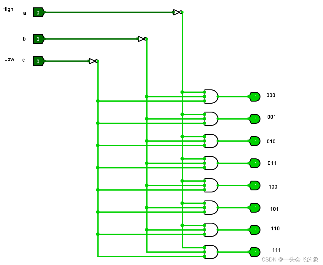
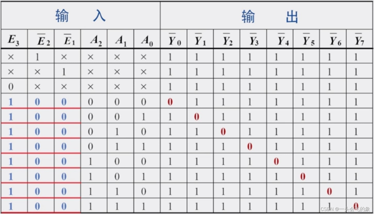
2,3-8译码器真值表:
3,生成RTL电路图:
代码如下
module Decoder_3to8 (
  input [2:0] input_bits,
  output [7:0] output_bits
);

  assign output_bits[0] = (input_bits == 3'b000) ? 1'b1 : 1'b0;
  assign output_bits[1] = (input_bits == 3'b001) ? 1'b1 : 1'b0;
  assign output_bits[2] = (input_bits == 3'b010) ? 1'b1 : 1'b0;
  assign output_bits[3] = (input_bits == 3'b011) ? 1'b1 : 1'b0;
  assign output_bits[4] = (input_bits == 3'b100) ? 1'b1 : 1'b0;
  assign output_bits[5] = (input_bits == 3'b101) ? 1'b1 : 1'b0;
  assign output_bits[6] = (input_bits == 3'b110) ? 1'b1 : 1'b0;
  assign output_bits[7] = (input_bits == 3'b111) ? 1'b1 : 1'b0;

endmodule
如图

4,测试代码:
// Copyright (C) 1991-2013 Altera Corporation
// Your use of Altera Corporation's design tools, logic functions
// and other software and tools, and its AMPP partner logic
// functions, and any output files from any of the foregoing
// (including device programming or simulation files), and any
// associated documentation or information are expressly subject
// to the terms and conditions of the Altera Program License
// Subscription Agreement, Altera MegaCore Function License
// Agreement, or other applicable license agreement, including,
// without limitation, that your use is for the sole purpose of
// programming logic devices manufactured by Altera and sold by
// Altera or its authorized distributors.  Please refer to the
// applicable agreement for further details.
// *****************************************************************************
// This file contains a Verilog test bench template that is freely editable to
// suit user's needs .Comments are provided in each section to help the user
// fill out necessary details.
// *****************************************************************************
// Generated on "12/15/2023 16:30:15"

// Verilog Test Bench template for design : Decoder_3to8
//
// Simulation tool : ModelSim (Verilog)
//

`timescale 1 ps/ 1 ps
module Decoder_3to8_vlg_tst();
// constants
// general purpose registers
reg eachvec;
// test vector input registers
reg [2:0] input_bits;
// wires
wire [7:0]  output_bits;

// assign statements (if any)
Decoder_3to8 i1 (
// port map - connection between master ports and signals/registers
	.input_bits(input_bits),
	.output_bits(output_bits)
);
initial
begin
$display("Running testbench");

	 // Test case 1
    input_bits = 3'b000;
    #10;
    if (output_bits !== 8'b00000001) $fatal("Test case 1 failed");
    // Test case 2
    input_bits = 3'b001;
    #10;
    if (output_bits !== 8'b00000010) $fatal("Test case 2 failed");
	 // Test case 3
    input_bits = 3'b010;
    #10;
    if (output_bits !== 8'b00000100) $fatal("Test case 3 failed");
	 // Test case 4
    input_bits = 3'b011;
    #10;
    if (output_bits !== 8'b00001000) $fatal("Test case 4 failed");
	 // Test case 5
    input_bits = 3'b100;
    #10;
    if (output_bits !== 8'b00010000) $fatal("Test case 5 failed");
	 // Test case 6
    input_bits = 3'b101;
    #10;
    if (output_bits !== 8'b00100000) $fatal("Test case 6 failed");
	 // Test case 7
    input_bits = 3'b110;
    #10;
    if (output_bits !== 8'b01000000) $fatal("Test case 7 failed");
	 // Test case 8
	 input_bits = 3'b111;
    #10;
    if (output_bits !== 8'b10000000) $fatal("Test case 8 failed");

end
always

begin
@eachvec;
end
endmodule
5,Modelsim仿真生成波形图: 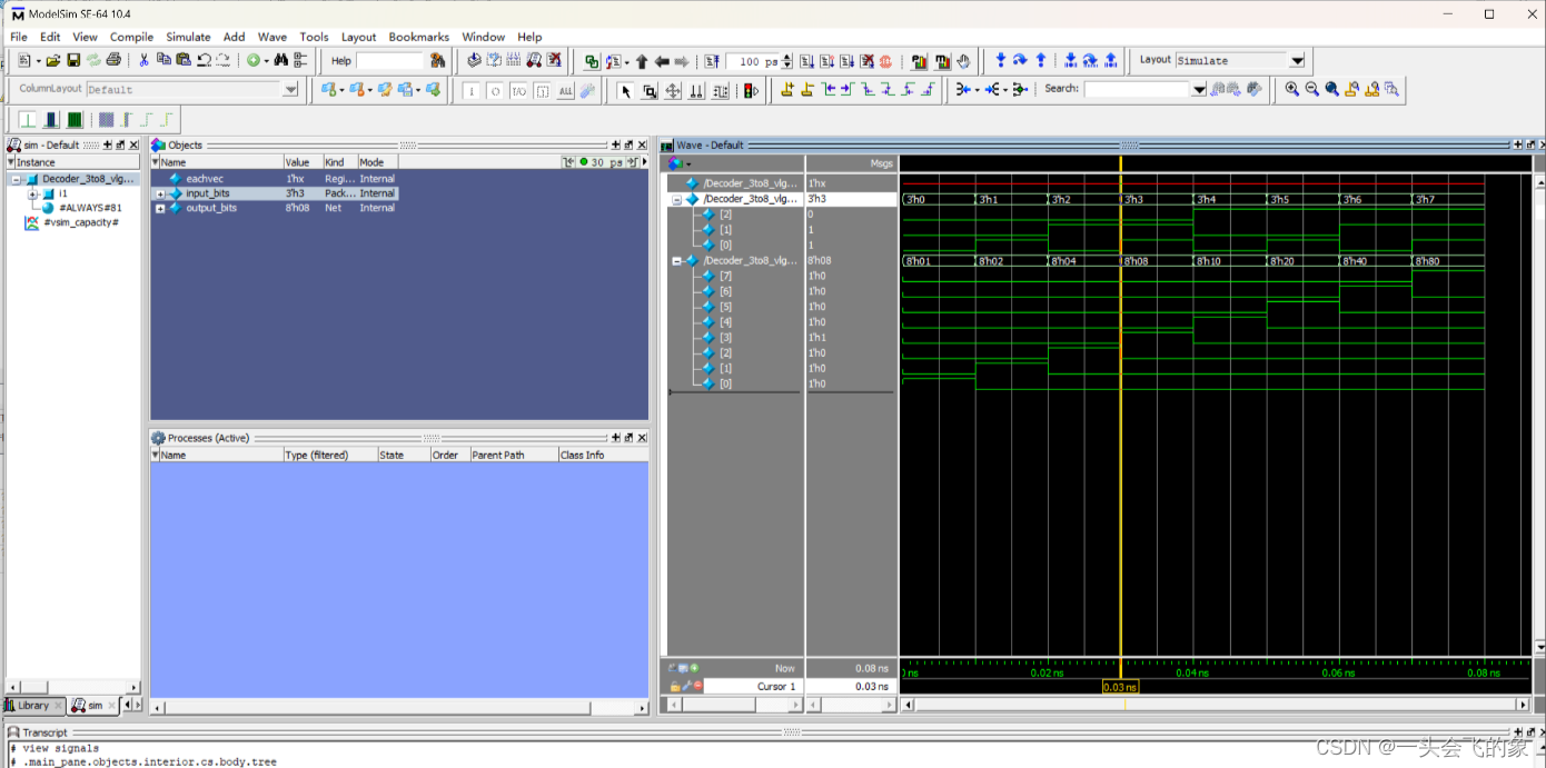
6,解决问题:
Verilog 综合生成的3-8译码器电路原理图与原始设计电路存在什么差异? 仿真测试生成的结果是否与真值表一致?
存在的差异为输入端与输出端,其余无差异。
仿真测试的结果经过一一检验也呈现出以下规则:
当 ABC = 000 时,Y0 = 1,其余输出线为0。
当 ABC = 001 时,Y1 = 1,其余输出线为0。
当 ABC = 010 时,Y2 = 1,其余输出线为0。
当 ABC = 011 时,Y3 = 1,其余输出线为0。
当 ABC = 100 时,Y4 = 1,其余输出线为0。
当 ABC = 101 时,Y5 = 1,其余输出线为0。
当 ABC = 110 时,Y6 = 1,其余输出线为0。
当 ABC = 111 时,Y7 = 1,其余输出线为0。
Verilog代码设计的3-8译码器模块的输出信号 为何要定义为 reg类型而不用默认wire(导线)类型?改成wire型是否可以? (即是否可以把 output reg [7:0] out 改为 output [7:0] out) 修改后会出现什么错误?为什么会出错?
两种类型差异:
reg 用于表示寄存器类型的变量,用于always模块内被赋值的信号,通常用于存储状态或时序逻辑。另一方面,wire 用于表示连续赋值的变量,用于always模块内未被赋值的信号,通常用于组合逻辑。因为3-8译码器模块的输出信号out是在always块中被赋值的,因此必须定义为reg类型。
可以改为wire类型,如果将out定义为wire类型,会出现多个驱动器的情况,从而导致错误。
三、全加器
(一)全加器的定义及其运算法则
1.定义:
全加器是一种数字电路组件,用于将两个二进制数的每一位和一个进位位相加。全加器与半加器不同,它可以处理三个输入:两个待加的二进制位和来自前一位的进位。全加器的输出包括一个和位(Sum)和一个进位位(Cout)。
2.运算法则:
一个1位全加器的运算法则如下:
1.输入:
A(加数的一位)
B(被加数的一位)
Cin(前一位的进位)
2.输出:
Sum(和位):A、B和Cin的异或结果,表示该位的二进制和。
Cout(进位输出):A、B和Cin的任意两个或三个的与运算结果,表示该位的进位。
(二)一、四全加器Logsim电路仿真以及Quartus模拟
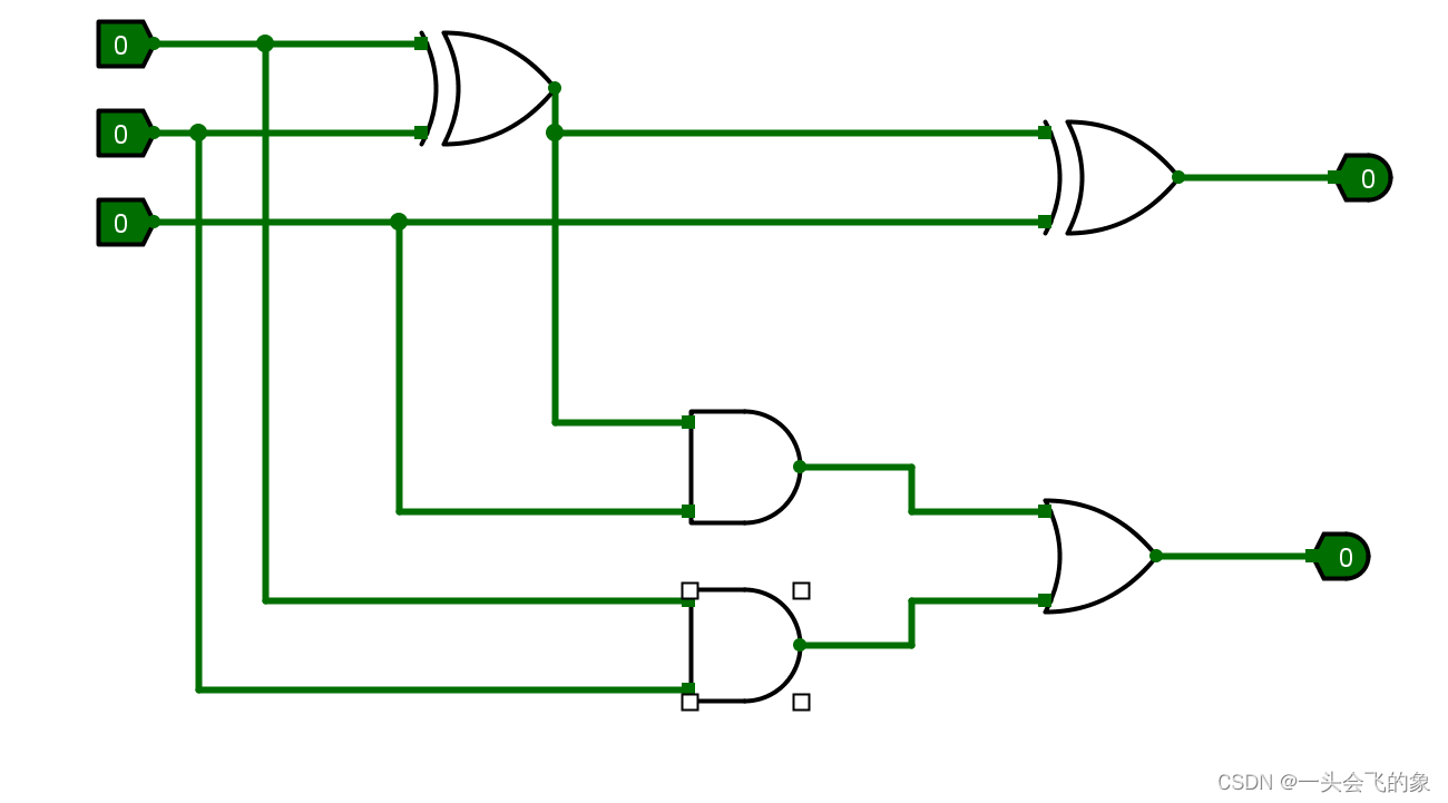
1,一位全加器
一位全加器logsim电路图:
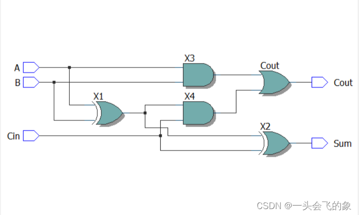
利用Verilog代码生成RTL电路图:
module FullAdder1Bit (

  input A, B, Cin,

  output Sum, Cout

);


  wire X1, X2, X3, X4;

  // 异或门

  assign X1 = A ^ B;

  assign X2 = X1 ^ Cin;

  // 与门

  assign X3 = A & B;

  assign X4 = X1 & Cin;

  // 或门

  assign Cout = X3 | X4;

  assign Sum = X2;


endmodule
2.四位全加器
电路图
利用Verilog代码生成RTL电路图:
module FourBitAdder(
  input [3:0] A,
  input [3:0] B,
  input Cin,
  output [3:0] Sum,
  output Cout
);

  wire [3:0] carry_out_intermediate;
  wire [3:0] sum_intermediate;

  FullAdder1Bit fa0 (.A(A[0]), .B(B[0]), .Cin(Cin), .Sum(sum_intermediate[0]), .Cout(carry_out_intermediate[0]));
  FullAdder1Bit fa1 (.A(A[1]), .B(B[1]), .Cin(carry_out_intermediate[0]), .Sum(sum_intermediate[1]), .Cout(carry_out_intermediate[1]));
  FullAdder1Bit fa2 (.A(A[2]), .B(B[2]), .Cin(carry_out_intermediate[1]), .Sum(sum_intermediate[2]), .Cout(carry_out_intermediate[2]));
  FullAdder1Bit fa3 (.A(A[3]), .B(B[3]), .Cin(carry_out_intermediate[2]), .Sum(sum_intermediate[3]), .Cout(carry_out_intermediate[3]));

  assign Sum = sum_intermediate;
  assign Cout = carry_out_intermediate[3];

endmodule

module FullAdder1Bit(
  input A,
  input B,
  input Cin,
  output Sum,
  output Cout
);

  assign Sum = A ^ B ^ Cin;
  assign Cout = (A & B) | (B & Cin) | (A & Cin);

endmodule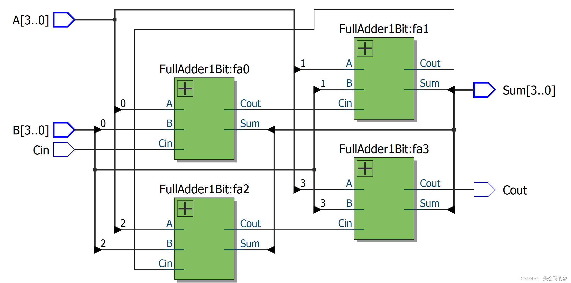
四、拓展实验
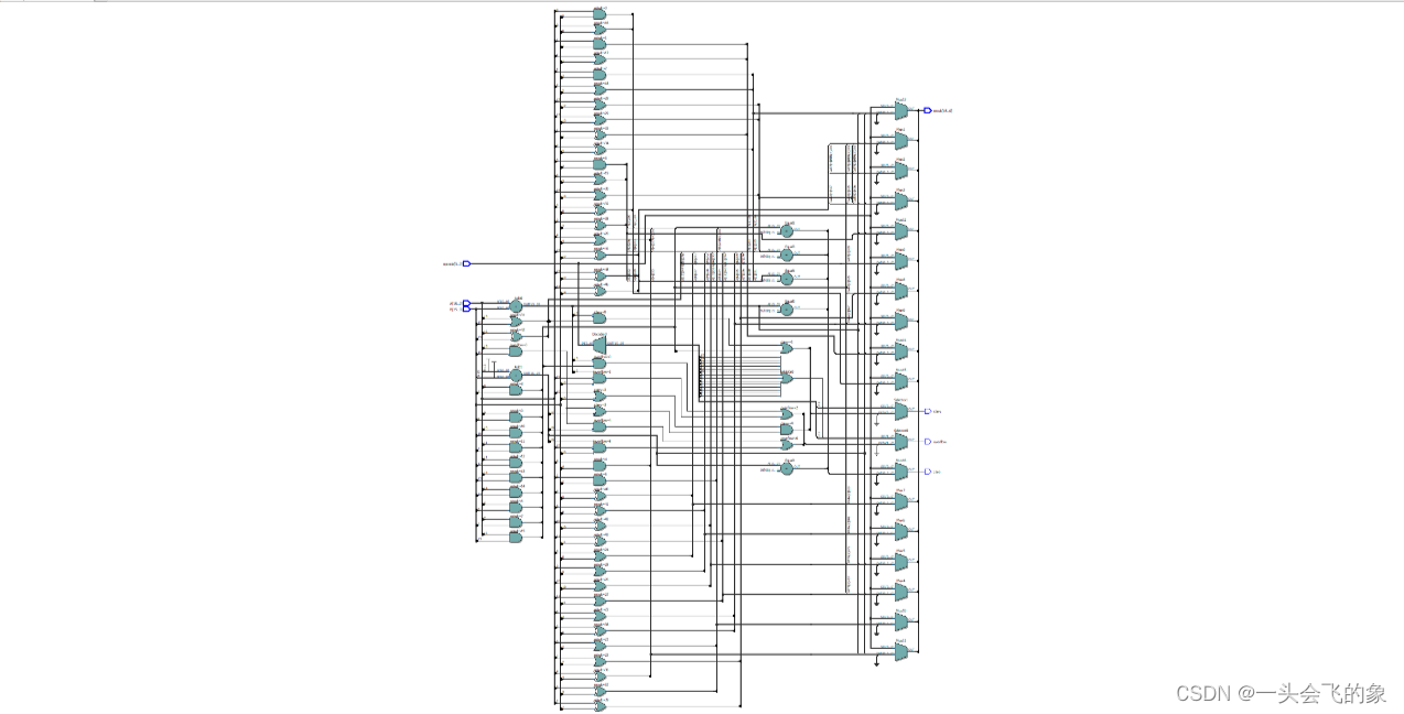
完成一个16位ALU(算术逻辑单元)的电路设计,采用Verilog设计模式,生成RTL电路。
代码如下
module SimpleALU_16bit (
    input wire [15:0] A,
    input wire [15:0] B,
    input wire [3:0]  opcode,
    output reg [15:0] result,
    output reg zero,
    output reg overflow,
    output reg carry
);

always @(A or B or opcode) begin
    case(opcode)
        4'b0000: // Addition
            begin
                result = A + B;
                zero = (result == 16'b0);
                overflow = (A[15] & B[15] & ~result[15]) | (~A[15] & ~B[15] & result[15]);
                carry = (A[15] & B[15]) | (~result[15] & (A[15] | B[15]));
            end
        4'b0001: // Subtraction
            begin
                result = A - B;
                zero = (result == 16'b0);
                overflow = (A[15] & ~B[15] & ~result[15]) | (~A[15] & B[15] & result[15]);
                carry = (A[15] | ~B[15]) & (~result[15] | (A[15] & ~B[15]));
            end
        4'b0010: // AND
            begin
                result = A & B;
                zero = (result == 16'b0);
                overflow = 1'b0;
                carry = 1'b0;
            end
        4'b0011: // OR
            begin
                result = A | B;
                zero = (result == 16'b0);
                overflow = 1'b0;
                carry = 1'b0;
            end
        4'b0100: // XOR
            begin
                result = A ^ B;
                zero = (result == 16'b0);
                overflow = 1'b0;
                carry = 1'b0;
            end
        // Add more operations as needed
        // ...

        default:
            begin
                result = 16'b0;
                zero = 1'b0;
                overflow = 1'b0;
                carry = 1'b0;
            end
    endcase
end

endmodule
电路图
测试代码
// Copyright (C) 1991-2013 Altera Corporation
// Your use of Altera Corporation's design tools, logic functions
// and other software and tools, and its AMPP partner logic
// functions, and any output files from any of the foregoing
// (including device programming or simulation files), and any
// associated documentation or information are expressly subject
// to the terms and conditions of the Altera Program License
// Subscription Agreement, Altera MegaCore Function License
// Agreement, or other applicable license agreement, including,
// without limitation, that your use is for the sole purpose of
// programming logic devices manufactured by Altera and sold by
// Altera or its authorized distributors.  Please refer to the
// applicable agreement for further details.
// *****************************************************************************
// This file contains a Verilog test bench template that is freely editable to
// suit user's needs .Comments are provided in each section to help the user
// fill out necessary details.
// *****************************************************************************
// Generated on "12/16/2023 22:05:26"

// Verilog Test Bench template for design : SimpleALU_16bit
//
// Simulation tool : ModelSim (Verilog)
//

`timescale 1 ps/ 1 ps
module SimpleALU_16bit_vlg_tst();
// constants
// general purpose registers
reg eachvec;
// test vector input registers
reg [15:0] A;
reg [15:0] B;
reg [3:0] opcode;
// wires
wire carry;
wire overflow;
wire [15:0]  result;
wire zero;

// assign statements (if any)
SimpleALU_16bit i1 (
// port map - connection between master ports and signals/registers
	.A(A),
	.B(B),
	.carry(carry),
	.opcode(opcode),
	.overflow(overflow),
	.result(result),
	.zero(zero)
);
initial begin
    $display("Starting 16-bit ALU Testbench");

    // Test Case 1: Addition
    A = 16'h1234;
    B = 16'h5678;
    opcode = 4'b0000; // Addition
    #10; // Wait for some time
    $display("Test Case 1 - Addition: Result = %h, Zero = %b, Carry = %b, Overflow = %b", result, zero, carry, overflow);
    // Test Case 2: Subtraction
    A = 16'hABCD;
    B = 16'h5432;
    opcode = 4'b0001; // Subtraction
    #10; // Wait for some time
    $display("Test Case 2 - Subtraction: Result = %h, Zero = %b, Carry = %b, Overflow = %b", result, zero, carry, overflow);

    // Add more test cases for other operations


  end

endmodule
结果
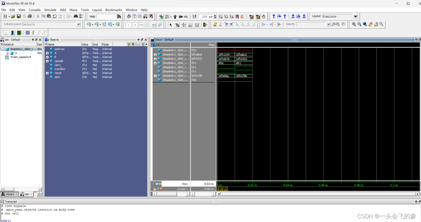


 1714
1714

 被折叠的 条评论
为什么被折叠?
被折叠的 条评论
为什么被折叠?
 到【灌水乐园】发言


