


- The differences between simulation and real hardware
1) The clk in sumulation is 50Mhz , in fact it is 24Mhz.
2) The pin assigned was according to the circuit schematic diagram.
Clk_sys –> pin B8 , rst_n –> pin F10 , RxD_in –> pin AB20 ,
TxD_out –> pin AA20 ,frame_err–> pin G17,parity_err –> pin G18.
3) In simulation process ,i had assumed that the system was reset when the rst_n port is in high level but in fact it was reseted when rst_n is in low level. This was puzzled me for a long time when i was using Chipscope observe the signal of top_module.
4) The sample paulse was 16 times of Baud rate while in fact it is 8 times. - Pre-and post Program framework
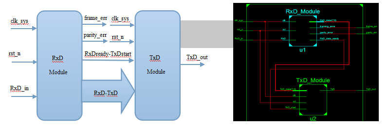
1) In order to generate TxD_start signal, RxD_data_ready is connected to TxD_start,The transmition is start when the receive process was done.
2) The frame and parity check result were transmite to the port frame_err and parity_err, both of them was used high level to respent the wrong state.
3) In order to observe the signal ,i had symplified some unnecessary port.
- Problems and Solutions in the Debugging process
1) Q:Lack of hardware test environment and PC has no USB to Serial driver
A: Borrow circuit board and rs232 cable from Mo,copy serial port unitity from Mo.
2) Q:Have no ideal about software’s problem
A:Connect DB9 pin 2 (TxD) and pin3 (RxD) directly and use the serial port unitity transmit macro to itself. The result indicated the software and driver was correct.
3) Q:How to find the problem after the debugging was failed
A:Lean xilinx tool of Chioscope to observe the value of inter register,using one day to learn how to use the Chipscope since i had never used it before.
4) Q:The problem of using Chipscope to compute the signal’ hold time
A:In Chipscope there is a clock signal for the whole running process,also X cursor and O cursor were also in there ,from the scale and clock we can compute the signal hold time and period of data. The period is clock frequency*(O cursor scale -O cursor scale). - The differences between simulation program and real program
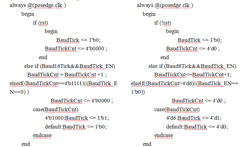
1) In simulation when the baudtickcnt was 4’b1000,it ok to transmite and receive ,while in in hardware it not received correctly. So i had to try another value ,after several attempt i found the 4’d6 was the correct number.
2) In simulation all registers and port was initialed when defining.but in real program those operation all placed in if(!rst) sentence.
3) change the style of program ,using symplfied name and changed the place of “begin” “ and” .making the program looks more concise and more understandable. - Notes of The Chipscope
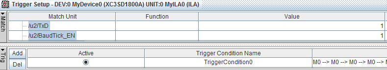
1) The Trigger Width in Trigger Parameter must keep the same with Net Connections chanel number.
2) In order to maintain the buffer of sample ,it better to chose the appropriate data depth .if there is not mamy signal to observer ,we can chose the large one,cantrary chose the small one.
3) After the *.cdc was added into project ,the implemtation becomes very slow especialy in translate process,so we must make if perfectly in channel number and signal which we want to observe.
4) If we had more than one devices in jtag chain ,there will be show in Anylze process, so we must chose the right one.
5) In anylsze process the trriger requirement was able to set more than one ,also the consequence of trigger also can be made.
Result of Debug
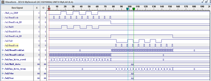
1) From Chipscope to observe signal value
From the picture above ,we can find that input signal RxD is the same with TxD,and the RxD_data is correspond with the tsr ,so we can conclude that this process is running correctly.
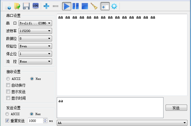
2) From Serial port unitity obseve result
From the picture above we can find that the transmition and receive is correct,and there also have the parity check ,Baud rate is 115200bps.Conclusion
From the Chipscope and Serial port unitity ,we can conclued that this program is running correctly.
UART 通信逻辑协议设计(3)
最新推荐文章于 2023-09-19 23:54:10 发布


 678
678

 被折叠的 条评论
为什么被折叠?
被折叠的 条评论
为什么被折叠?
 到【灌水乐园】发言


