


- Basic knowledge of RAM
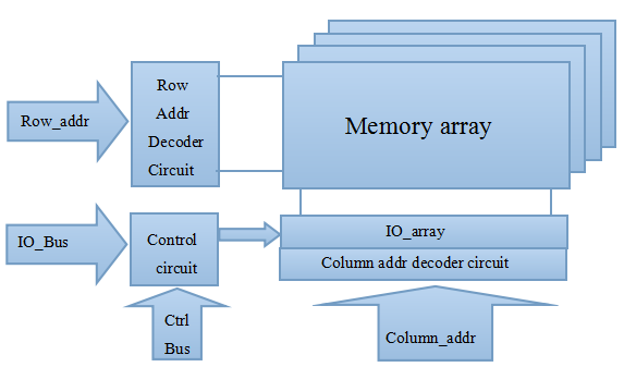
1) The fundamental structure of RAM include that address bus,data bus,control bus and decoding circuit of each bus.There is two type of decoding circuit connect at the address bus,the one is column address decoder,and the other is row address bus.The construction of Basic Ram shows in Figure 1.
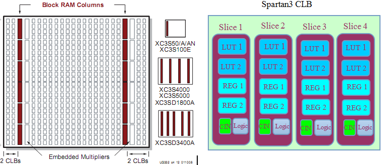
2) There are 4 important part in FPGA.CLB,IOB,PIR and Block RAM,among these resources CLB is the most import one.it has contains 4 Slice in Spartan 3a. Every slice contains 2 LUT,2 Reg,and cin or arithmetic logic. Also the Slice was defined into two type of is,the first one is SliceM which was used to distributed RAM or Block RAM,the other one is SliceL which was only used in LUT. There are two type of RAM in Xilinx FPGA,The distributed RAM and Block RAM. There are 4 column RAM and each column has 20-22 RAM blocks,total 1512Kbits RAM in Extended Spartan-3a FPGAs. Each block RAM read and write speed up to 240Mhz.The Figure 2 shows the Block RAM’ location and number in Spartan3a,Figure 3 shows the basic architecture of CLB.
- IP Core Block RAM Configuration
1) There have 3 type of RAM in xilinx IP Core,they are single port RAM,simple dual port RAM,true dual port RAM.The single port RAM can be operated in write or read model but it’s will be not valid at the same time.The dual port RAM can write at the port A,read at port at port B.whatmore,it can be read or write at the same time.
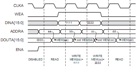
2) The port can be set in 4 model when we use it. When in the write first model,the data will be simultaneously written into memory and driven on the data output,while in read first model the data will be stored and will not be driven on the data output.The timing operation is shown in Figure 4.
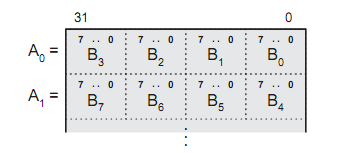
3) There are lots of Block RAM in Spartan 3a.if the Block was not enough to use,the distributed RAM can as a supplement.so we can configure our RAM flexibly the internal Block RAM amount 1512Kbits .if we need put 256 data and each data was in hex into RAM,then we need 256*8*8=16384 bits.if we use 8bits port ,then we assumed that 16384 = 8*4096 ,the address bus must be 12bits.the data stored in the RAM as shown in Figure 5.
Using XILINX IP Core Block RAM (1)
最新推荐文章于 2021-12-17 10:13:02 发布


 1万+
1万+


 被折叠的 条评论
为什么被折叠?
被折叠的 条评论
为什么被折叠?
 到【灌水乐园】发言


