


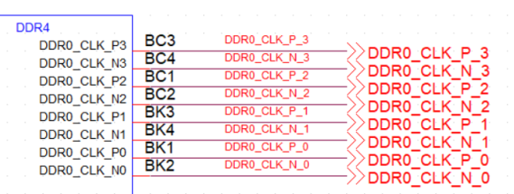
SDRAM Differential Clock :Differential clocks signal pairs , pair perrank . The crossing of the positive edgeand the negative edge of theircomplement are used to sample thecommand and control signals on theSDRAM
SDRAM差分时钟:差分时钟信号对,每列对。补码的正边缘和负边缘的交叉用于对SRAM上的命令和控制信号进行采样。
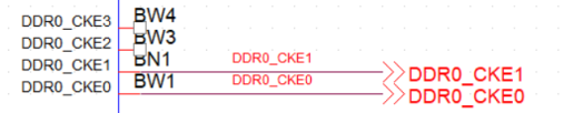
Clock Enable : ( 1 per rank ) . Thesesignals are used to :Initialize the SDRAMS duringpower-up .Power-down SDRAM ranksPlace all SDRAM ranks into and outof self-refresh during STR( Suspend to RAM ) .
时钟启用:(每列1个)。这些符号用于:在加电期间初始化SDRAM。关闭SDRAM列。在STR(挂起到RAM)期间,将所有SDRAM列放入或移出自刷新。
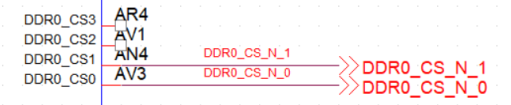
Chip Select : ( 1 per rank ) . Thesesignals are used to select particularSDRAM components during the activestate . There is one Chip Select for eachSDRAM rank
芯片选择:(每个等级1个)。这些符号用于在活动状态期间选择特定的DRAM组件。每个SDRAM等级有一个芯片选择
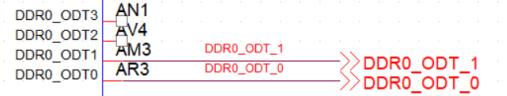
On Die Termination : ( 1 per rank ) .Active SDRAM Termination Control
片上终端:(每列1个)。主动SDRAM终端控制
Address : These signals are used toprovide the multiplexed row andcolumn address to the SDRANA [ 16 : 14 ] use also as commandsignals , see ACT _ N signaldescriptionA10 is sampled during Read / Writecommands to determine whetherAutoprecharge should beperformed to the accessed bankafter the Read / Write operationHIGH : Autoprecharge ;LOW : no Autoprecharge )A10 is sampled during a Prechargecommand to determine whetherthe Precharge applies to one bankA10 LOW ) or all banks ( A10HIGH ) . If only one bank is to beprecharged , the bank is selectedby bank addressesA12 is sampled during Read andWrite commands to determine ifchop( on-the-fly ) will be performed( HIGH , no burst chopLOW : burst chopped )DDR0 _ MA [ 16 ] uses as RAS # signaDDR0 _ MA15 ] uses as CAS # signaDDR0 _ MA [ 14 ] uses as WE # signalDDR1 _ MA [ 16 ] uses as RAS # signalDDR1 _ MA [ 15 ] uses as CAS # signalDDR1 _ MA ( 14 uses as WE # signal
地址:这些信号用于将多路复用的行和列地址提供给SDRANA[16:14],也用作命令信号,参见ACT_N信号描述A10在读/写命令期间采样,以确定在读/写入操作之后是否应对访问的存储体执行自动预充电HIGH:自动预充电;LOW:无自动预充电)A10,以确定预充电是应用于一个存储体A10 LOW)还是所有存储体(A10HIGH)。如果只有一个存储体要被预充电,银行由银行地址选择在读写命令期间对A12进行采样,以确定是否将执行chop(动态)(HIGH,no-brust chopLOW:突发斩波)DDR0 _ MA[16]用作RAS#signaDDR0 _MA15]用作CAS#signa DDR0 _MA[14]用作WE#signalDDR1 _ MA[14]作为RAS#signalDDR1 _ MA[15]用作CAS#signal DDR1 _MA(14用作WE#信号
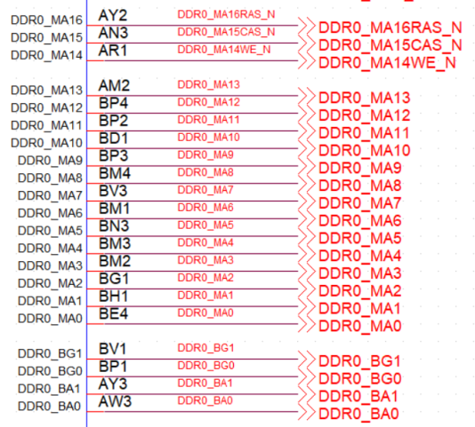
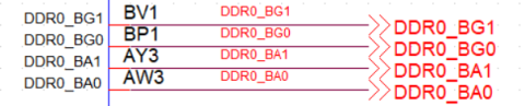
Bank Group : BG [ 1 : 0 ] define to whichbank group an Active , reading , Writeor Precharge command is beingappliedBGO also determines which moderegister is to be accessed during a MRScycle
存储体组:BG[1:0]定义将Active、read、Write或Precharge命令应用于哪个存储体。GO还确定在MRS周期中要访问哪个模式寄存器
Activation Command : ACT # HIGHalong with CS _ N determines that thesignals addresses below havecommand functionality .
激活命令:ACT#HIGH和CS_N确定以下信号地址具有命令功能。

Data Strobes : Differential data strobepairs . The data is captured at thecrossing point of DQS during readingand write transactionsExample : DDRO-DQSPO refers toDQSP Of DDR channel O , Byte 0 .数据选通:差分数据选通对。读取和写入事务期间,数据在DQS的交叉点捕获。示例:DDRO-DQSPO指DDR通道O的DQSP,字节0。

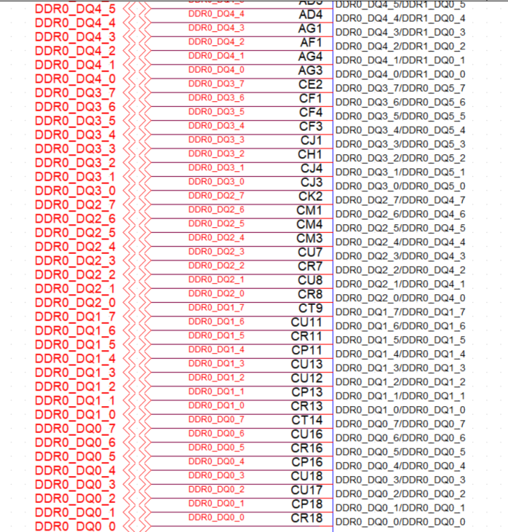
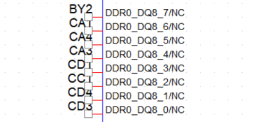
Data Buses : Data signals interface tolthe SDRAM data busesExample : DDR0 DQ2 [ 5 ] refers toDDR channel 0 , Byte 2 , Bit 5 .
数据总线:数据信号接口至SDRAM数据总线示例:DDR0 DQ2[5]指DDR通道0,字节2,位5。
ECC DATA Buses
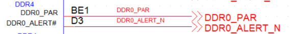
Command and Address ParityThese signals are used for paritycheck
命令和地址奇偶校验这些信号用于奇偶校验
Alert : This signal is used at commandtraining only . It is getting theCommand and Address Parity errorflag during training . CRC feature is notsupported .
警告:此信号仅用于命令训练。它在训练过程中收到命令和地址奇偶校验错误标志。不支持CRC功能。
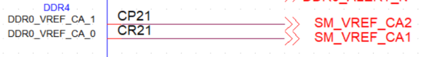
Memory Reference Voltage forCommand and Address
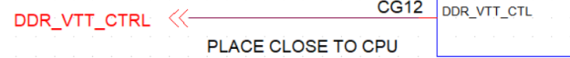
System Memory Power GateControl : When signal is highplatform memory VTT regulator isenable , output high .When signal is low-disables theplatform memory VTT regulator in C8and deeper and $ 3 ( H SKU only )
复位


 1989
1989

 被折叠的 条评论
为什么被折叠?
被折叠的 条评论
为什么被折叠?
 到【灌水乐园】发言


