


 本文讲述了使用Arduino和SSD1306OLED显示屏的初次尝试,涉及硬件连接、SPI通信、驱动时序分析、初始化设置、字符显示以及取模方法,强调了数据手册和正确接线的重要性。
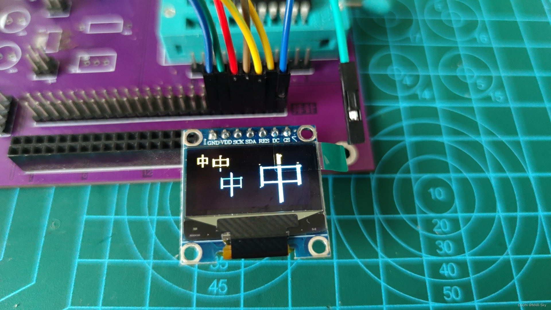
第一次尝试点亮
程序代码地址,密码:1234。
买了一个两色的oled,然后下载了资料,手里有一个8266的arduino,所以为了方便就直接用了。使用arduino主要原因,单片机keil太大,来回找文件修改引脚比较麻烦。实际在spi的通信方面的原理都是一样。
首次尝试,遇到问题,
1,资料中的引脚号需要修改
2,点阵取模得到的各种字符的**font.h文件和工程文件(.ino)**需要放在同级文件夹内。介绍中建议是放在arduino的lib文件夹中,但为了方便,也可以直接读取,所以直接移动一个文件夹就行。而且这个只是示例字符文件,没必要保存。
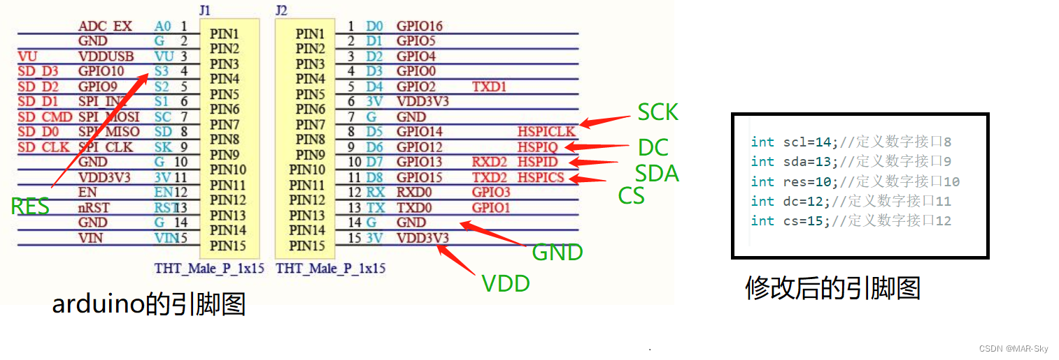
3,需要注意,如果只是给了电源电压,OLED也是不会亮的。个人本来怀疑屏坏了,后来接上信号线后,下完程序,发现能正常显示,不知道为什么手机拍的颜色有点儿失真。
驱动SSD1306读取工作时序分析
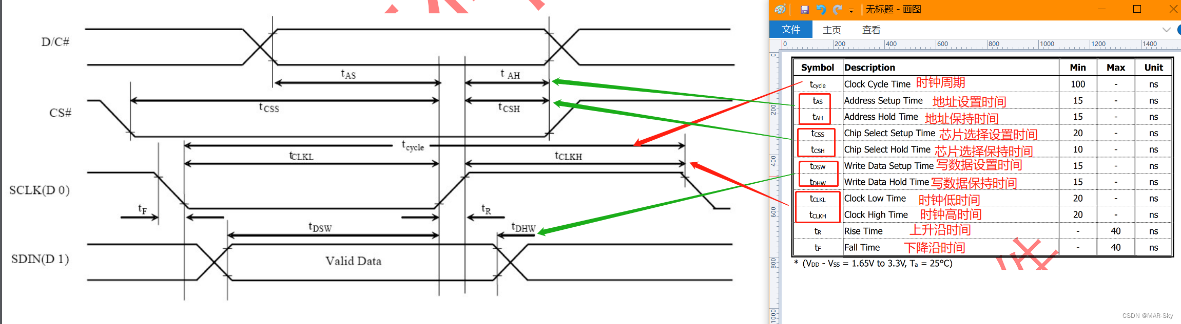
从时序图中可以看出,主要包含6种时间:时钟周期,地址设置时间,芯片选择时间,读写数据时间,时钟周期中高低时间,上升下降沿时间
时钟周期:大于100ns=10-7s,也就是时钟频率小于10MHz,
时钟周期中低电平和高电平时间:大于15ms
地址(数据/命令)设置/保持时间、写/读数据时间:设置是传送数据还是传送命令,会发现两种时间的值是一样的。从根本上来讲写入命令和写入地址都是进行信息传递。
上升沿和下降沿时间:最大是40ns,理论上,理想的波形应该是矩形波,也就是上升和下降沿是0s。
时间的整体分析:
首先,第一个时间是片选时间cs起作用,毕竟没选择好设备,发送数据或命令都无意义;由于数据或命令的传送都是在时钟的上升沿完成,所以在上升沿的那段时间,必须保证D/C(数据/命令)和数据传送的电平稳定。
常用设置分析(实际就是对驱动SSD1306的理解)
OLED基本参数
0.96寸双色显示屏,支持IIC和spi通信,128*64pixels,8page显示内存,相当于将屏幕的行按照字节数分为8份
驱动手册的命令使用和查找方式
来源:可以通过很多途径,有些只是给了部分常用内容,若想知道详细的手册可以去一些关于硬件手册的网站(例如半导小芯等)查询下载,下面是截取一部分命令表格说明使用方式
初始化使用的命令
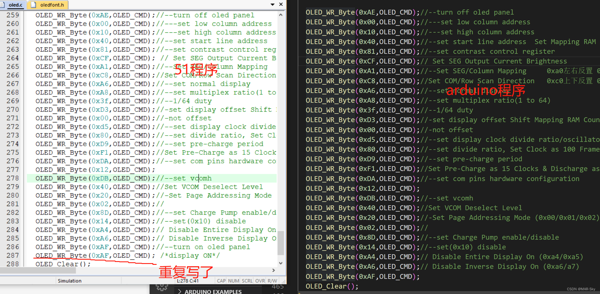
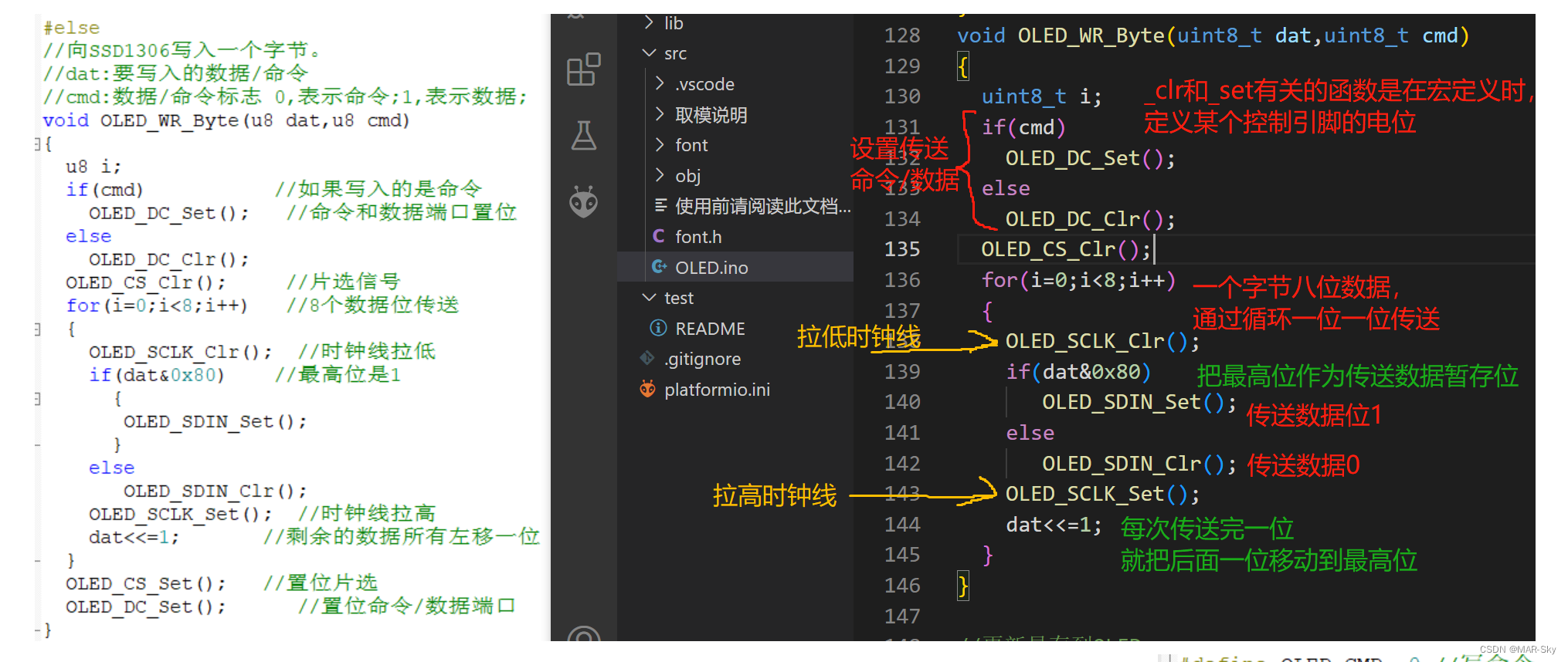
下面的OLED_WR_Byte是定义的函数,MCU把程序写入到驱动,进而控制显示屏。不同的编程软件和MCU来看,程序的表现形式可能不同,但基本命令是一样的。这些命令都可以通过手册找到。
几个比较重要和常需要变化的命令:
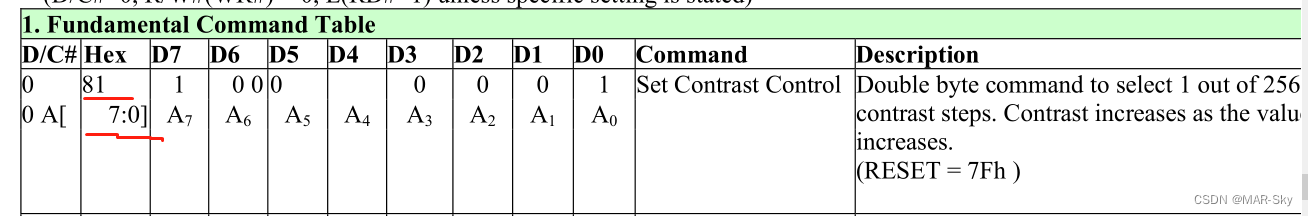
1,设置对比度:这里感觉就是亮度,命令如下图,根据上面查看手册命令的方式,可以知道需要发送两次命令,第一次的0x81只是告诉驱动下个自己的命令是对比度的值
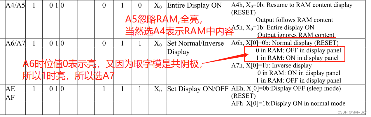
2,显示有关命令包括屏幕打开(AF)/关闭(AE),数据位0(A7)还是1(A6)亮,上下,左右(26/27)滚动,都可通过手册中查到
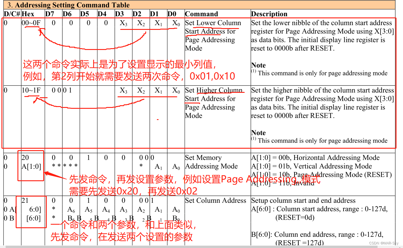
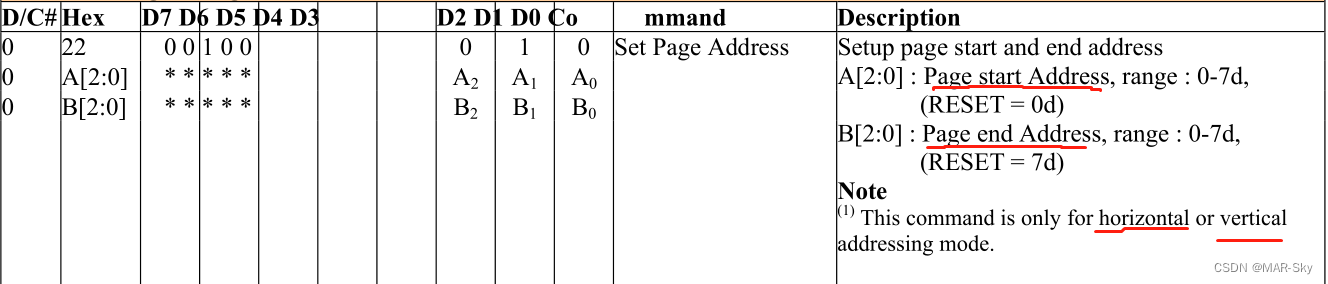
地址显示位置命令
参考手册中9 Command Table中的3 Addressing Setting Command Table
这个控制画面的显示位置,需要控制内存地址的模式,列开始,行开始和结束
首先知道,有8个page,相当于可以存储8个128*64的显示缓存
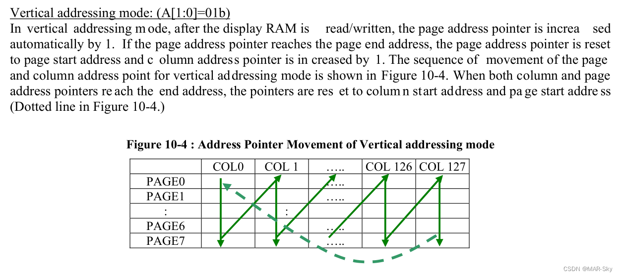
内存地址模式有三种:Page addressing mode ,Horizontal addressing mode,Vertical addressing mode
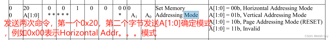
	OLED_WR_Byte(0x20,OLED_CMD);//-Set Page Addressing Mode (0x00/0x01/0x02)
	OLED_WR_Byte(0x02,OLED_CMD);//也就是A[1:0]=10b
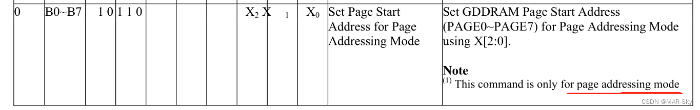
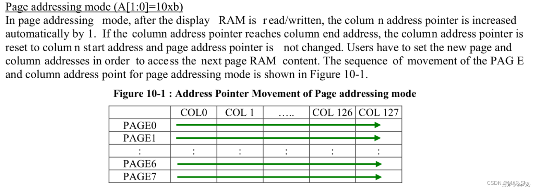
Page addressing mode模式
这种模式:到每个page结尾指针会自动到开始,但并没有到下一个page
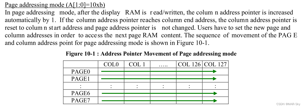
这种模式设置起始列位置需要两个命令
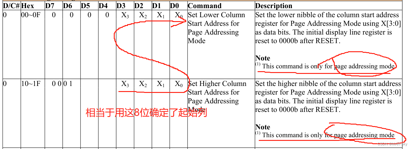
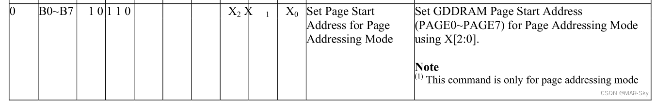
设置page起始
Horizontal addressing mode
这种地址分布是到行结尾自动跳转到开始,且page也自动到下一个,到最后page结束又会指向第一个page。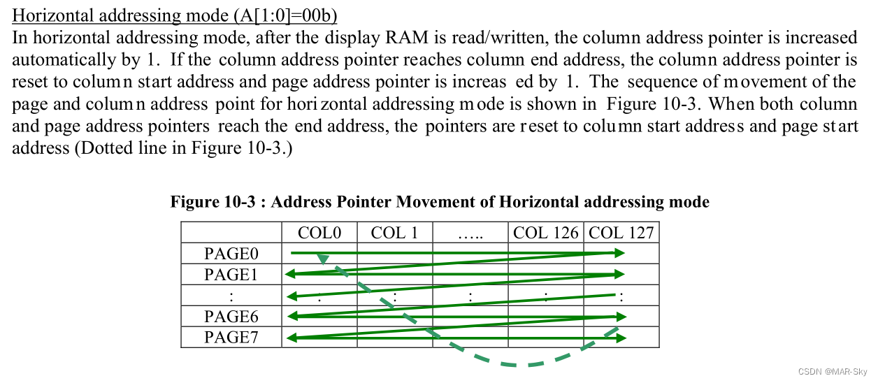
设置列的起始和结束

设置page的起始
下面模式的地址分布从上到下,从左到右
字节数据(data/command)传送
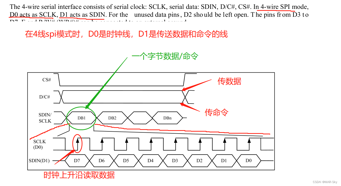
下图程序中的设置和上图的数据传送时序图刚好匹配
字符数据显示
整体方法,对字符取模,在初始化设置完成的情况下,将字模矩阵数据传入驱动
ASCII字母标
	void OLED_Set_Pos(unsigned char x, unsigned char y)
{
	/*
	x±íʾ¿ªÊ¼ÏÔʾµÄÏñËØÆðʼλÖÃ
	y±íʾÏÔʾÔÚÄÇÒ»Ò³
	*/
	OLED_WR_Byte(0xb0+y,OLED_CMD);     //ÉèÖõØÖ·Ò³£¬y¡Ê[0£¬7]
	//½«ÏÔʾµÄ¿ªÊ¼µØÖ·ÖеĸßËÄ룬ºÍµÍËÄλ·Ö¿ªºóдÈë¸øOLED
	//¶ø8λµÄ·¶Î§
	OLED_WR_Byte(((x&0xf0)>>4)|0x10,OLED_CMD);  //ÉèÖÃÏÔʾλÖᪿªÊ¼ÁеØÖ·µÄµÍËÄλ
	OLED_WR_Byte((x&0x0f)|0x01,OLED_CMD);    //ÉèÖÃÏÔʾλÖᪿªÊ¼ÁеØÖ·¸ßËÄλ
}
/*参数含义(c51程序)
x,显示位置的横坐标x
y,显示位置纵坐标y
下面程序中几个参数是宏定义过的,
size=16(字模16*8),OLED_DATA=1(传送的是数据)
*/
void OLED_ShowChar(u8 x,u8 y,u8 chr)
{
	unsigned char c=0,i=0;
		c=chr-' ';					//字符在ascii位置
		if(x>Max_Column-1)  //如果显示到最右边
			{x=0;y=y+2;}	//到最左边,向下移动两个像素
		if(SIZE ==16)
			{
			OLED_Set_Pos(x,y);	//设置字符显示的起始地址
			for(i=0;i<8;i++)    //将一个字节的8个位按位传送出去
				OLED_WR_Byte(F8X16[c*16+i],OLED_DATA);   //F8X16是取字模的数组,这个传送方式要看具体的取模方式
			OLED_Set_Pos(x,y+1);  //向下移动一个地址页page
			for(i=0;i<8;i++)
				OLED_WR_Byte(F8X16[c*16+i+8],OLED_DATA);
			}
		else {
				OLED_Set_Pos(x,y+1);
				for(i=0;i<6;i++)
				OLED_WR_Byte(F6x8[c][i],OLED_DATA);

			}
}
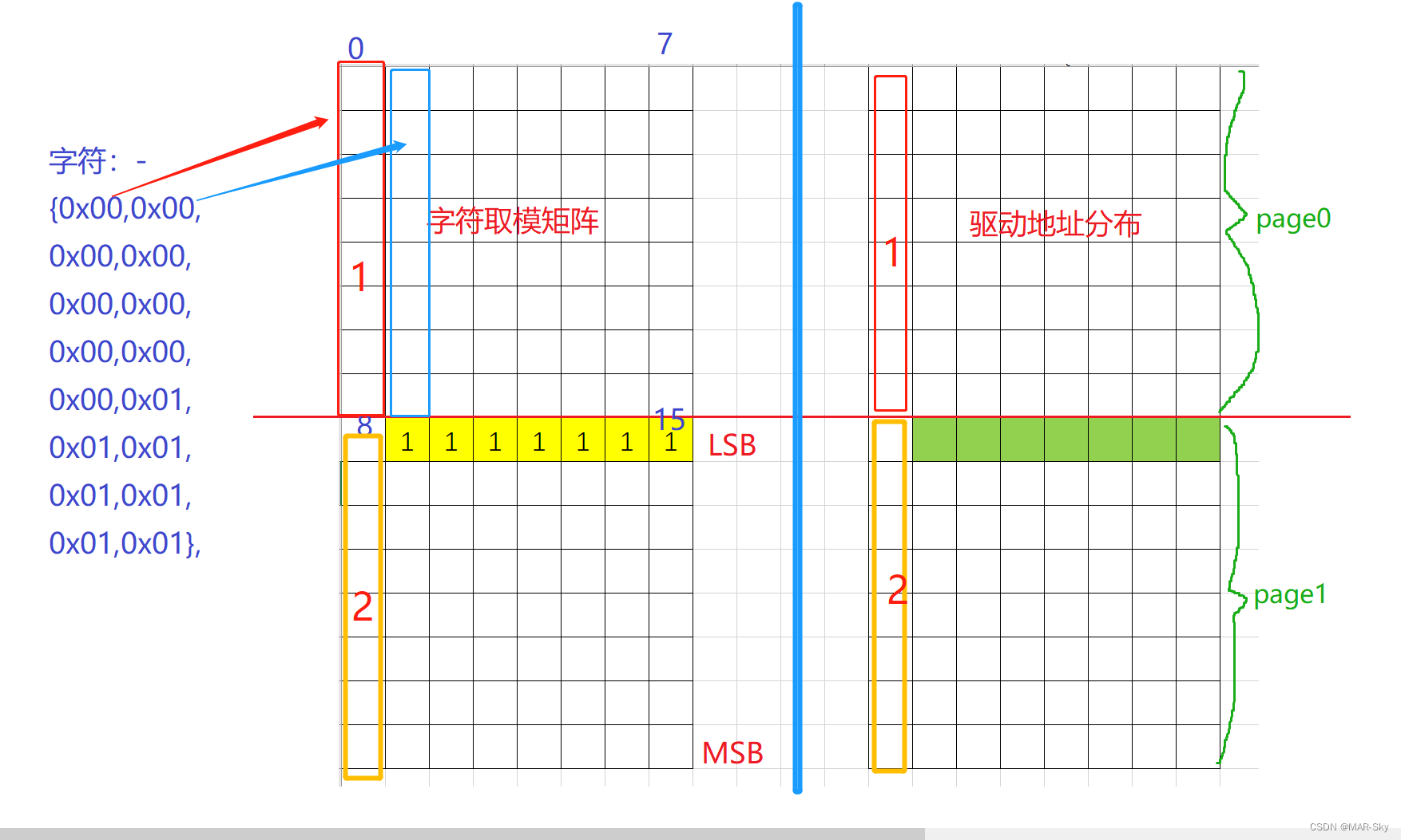
想要分析上面显示代码的位置分配原因,需要考虑取字模的方式
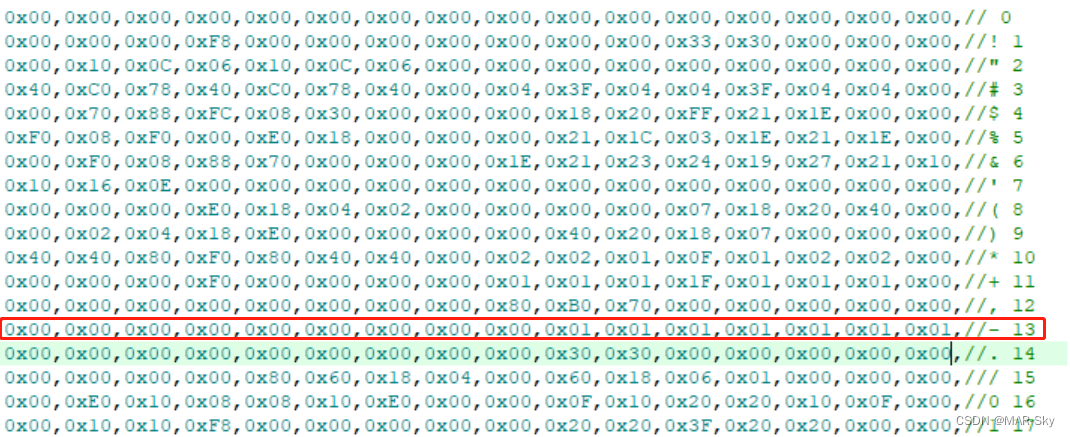
{0x00,0x00,0x00,0x00,0x00,0x00,0x00,0x00,0x00,0x01,0x01,0x01,0x01,0x01,0x01,0x01},/*"-",0*/
/* (8 X 16 , 隶书 )*/
从字模库中找到字符“-”的矩阵反推出取模方式
取模方式,低位先取到
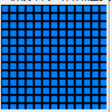
下面是驱动中的像素分配地址方式,

			/*传入显示的数据*/
			OLED_Set_Pos(x,y);	//设置字符显示的起始地址
			for(i=0;i<8;i++)    //将一个字节的8个位按位传送出去
				OLED_WR_Byte(F8X16[c*16+i],OLED_DATA);   //F8X16是取字模的数组,这个传送方式要看具体的取模方式
			OLED_Set_Pos(x,y+1);  //向下移动一个地址页page
			for(i=0;i<8;i++)
				OLED_WR_Byte(F8X16[c*16+i+8],OLED_DATA);

			/*设置地址OLED_Set_Pos中的纵轴方向设置,下面手册中命令可以看出*/
			OLED_WR_Byte(0xb0+y,OLED_CMD);
这里设置的特定的模式,第二个16进制位表示进入的page
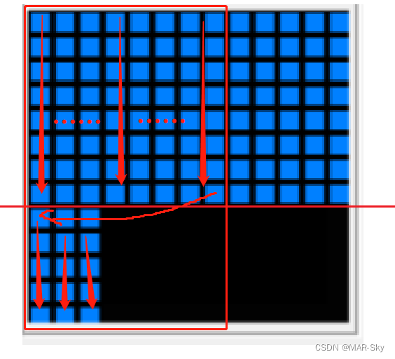
上面一段代码的写入字节过程如下图所示,F8X16[c*16+i],其中c*16是一个字符占16字节,所以得到了字符索引,一个字符中的16个字节需要按字节送入,所以才有偏置i。当前8个字节的数据传送完,需要在驱动中换page。**OLED_Set_Pos(x,y+1);**的作用不只是换一行,而是以字节为单位换行,也就是换page
字符串传送
//实际上就是将字符串看作指针,对每个字符遍历显示,直到最后一位
void OLED_ShowString(u8 x,u8 y,u8 *chr)
{
	unsigned char j=0;
	while (chr[j]!='\0')
	{		OLED_ShowChar(x,y,chr[j]);
			x+=8;   //每个字符横向占8个位
			//到屏幕最右边若不够放下一个字符,会跳转到下一行显示,y+=2是因为,一个字符高度是两个字节
		if(x>120){x=0;y+=2;}
			j++;
	}
}
个人总结
整体来看,好像有很多命令。但按照手册中的介绍初始化还是很方便的。
数据手册的查看很重要。显示屏的正常显示需要很清楚知道硬件取模和软件驱动的数据写入方式。
屏幕的显示很依赖字符或图片的取模方式和硬件的实际接线方式。
对于驱动的控制有两种方式:传入命令或数据。传入命令或数据的判断是通过给显示屏一个引脚高低电平控制的


 1823
1823

 被折叠的 条评论
为什么被折叠?
被折叠的 条评论
为什么被折叠?
 到【灌水乐园】发言


