


首先是来看看一个实际的问题:
我想知道这个的电压是多少?
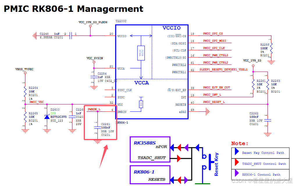
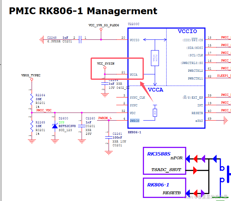
对于 rk806 的所有的 io 的电压特性都可以在 数据手册中找到。
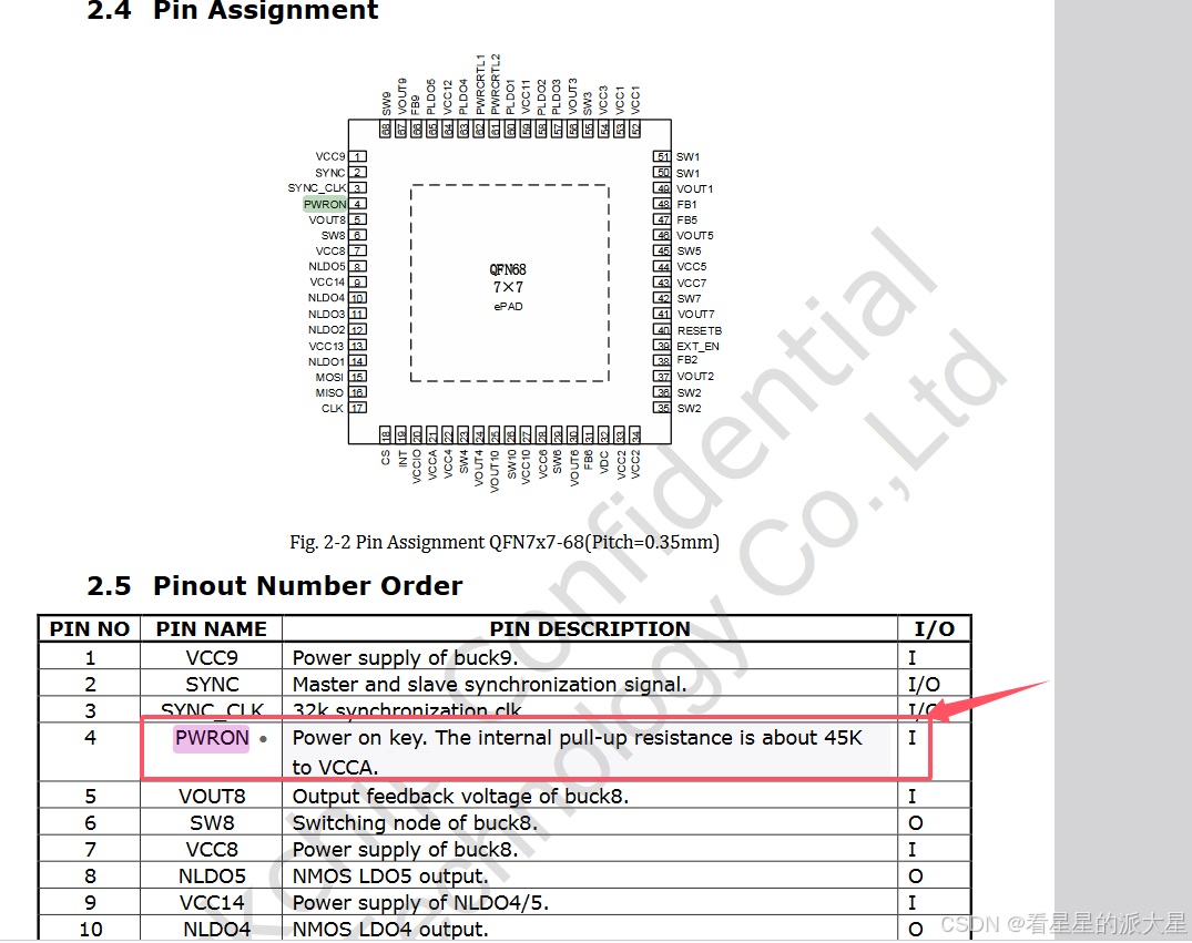
PWRON可以看到这个引脚是上拉 VCCA的。
那么 VCCA是什么呢?
就是 底板上来的 4V
-----------------------------------------
然后就是关于 电源域的内容。
网上的资料如下:
大致的逻辑是这样的,首先要看CPU的模块 ,需要什么电压,
然后 通过i2c 来设置 rk806 的 链接cpu 的引脚输出的电压。
这个设置 可以在 设备树中进行。
这就是所谓的电源域的配置。
--------------------------------------------------------------------------------------------------------------------------------
rk806 的电压 我比较明白了。
但是 cpu 的gpio 的电压是多少我一直没有搞明白。
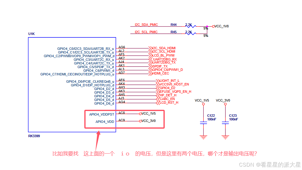
比如 rk3399
它这里 0.9, 1.8 , 3.3 都有,你说 上面的 io 口的电压是多少呢?
那么我就去看看 cpu 的数据手册,看看有没有说明。
查了, usb_AVDD_3V3
查了, TYPEC1_U2VBUSDET
但是 都没有说明。
看了看瑞芯微官方的 文档解释,有个 大致的了解。
我使用的是rk3399
来看一下 官方文档的截图吧。
也就是说,要想知道 cpu 上的某个gpio 是高电平,还是低电平,首先是要确定 这个io 的电源域。
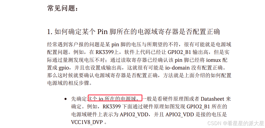
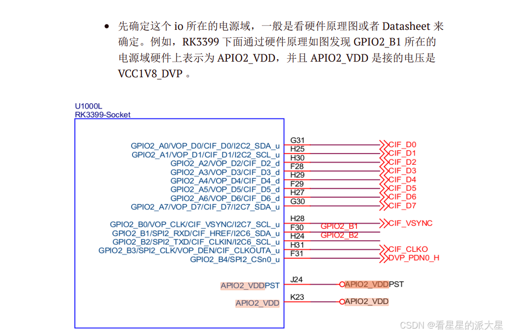
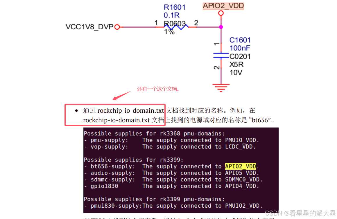
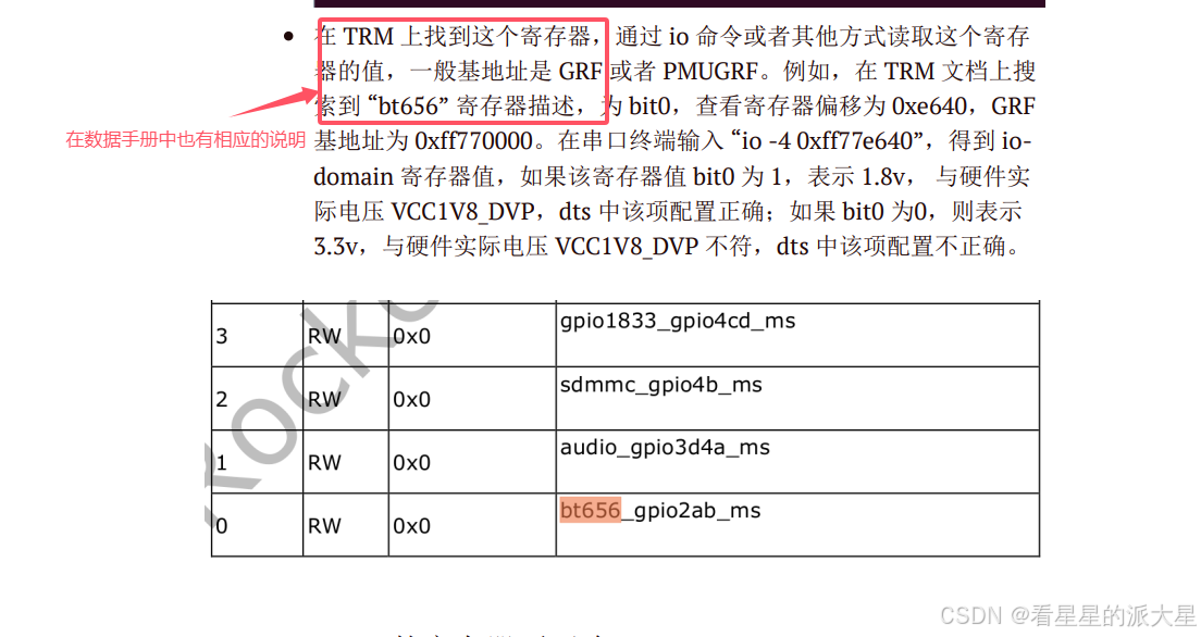
那么我来看看 这个 txt 文档吧。
rk3399_linux_sdk_v2.0/kernel/Documentation/devicetree/bindings/power/rockchip-io-domain.txt
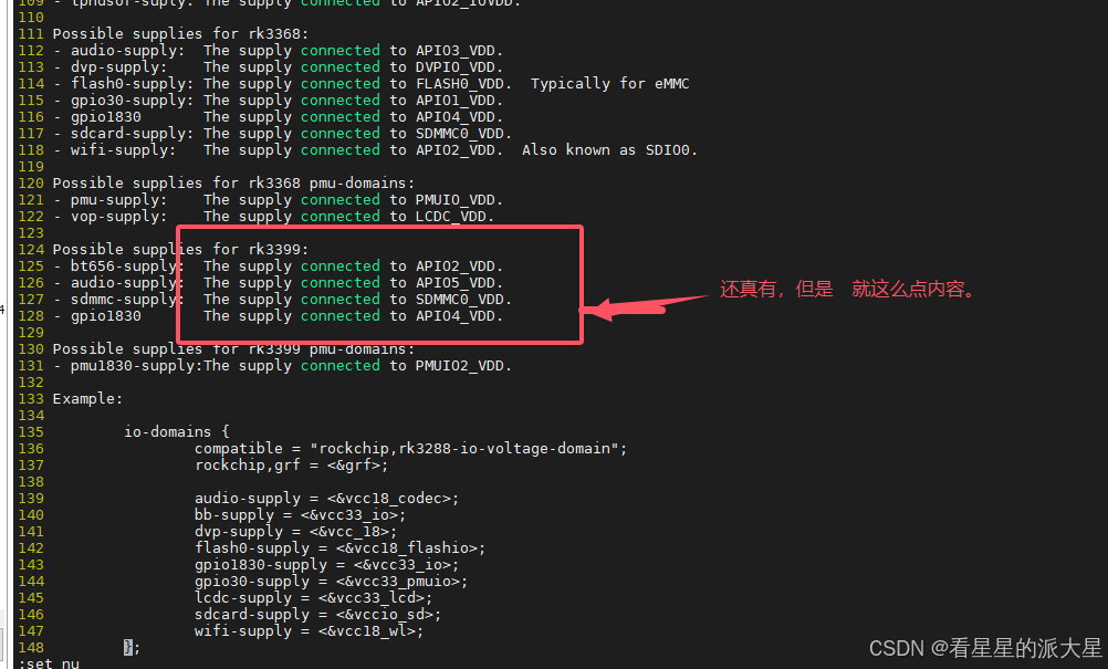
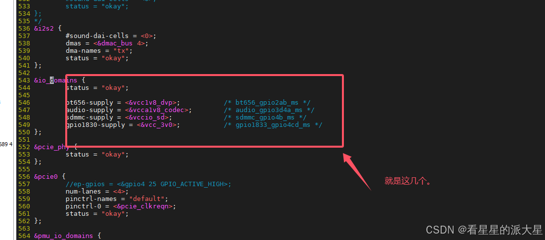
这几个 的配置 我在设备数中也是可以找到的。
kernel/arch/arm64/boot/dts/rockchip$ vim itop-3399_linux-core.dtsi
这里我不理解 , 为什么 就这么几个 电压域呢?
--------------------------------------------------------------------------------------------------------------------------
然后再来看一个我对 电压域的 理解。
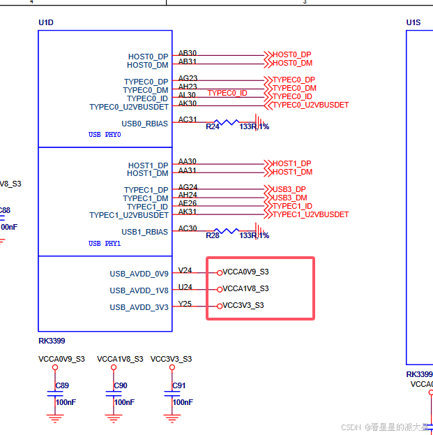
在核心板的原理图中。
这个,我还真就在数据手册中找到了。
看到了吧,这两个电压配合起来, 才能够确定 io 是 3.0V的电压。
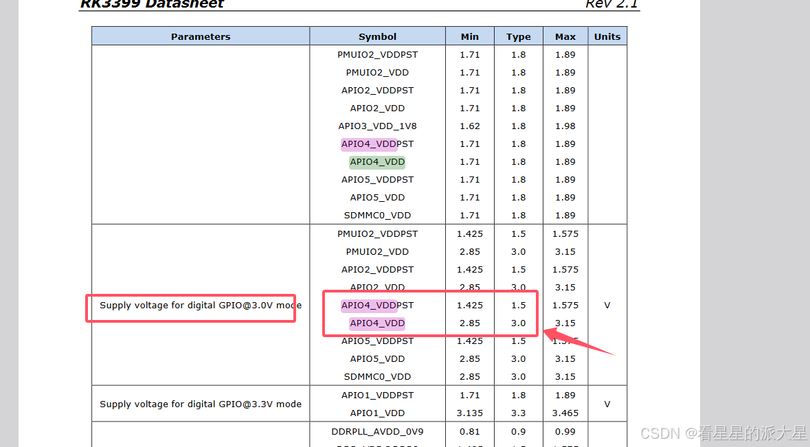
这里面涉及到一个 rk808 的配置
这里有个 点 ,很容易混淆, 就是 cpu 电压域的配置与 rk809 的配置。
感受一下 rk809 的配置, 在设备树中也有。
kernel/arch/arm64/boot/dts/rockchip$ vim itop-3399_linux-core.dtsi
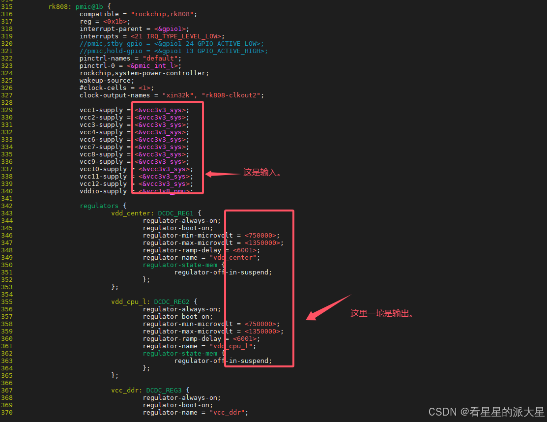
总结: rk809 跟电压域是不一样的。感觉。
-----------------------------------------------------------------------------------------------------------
然后来看一下 rk3568 的关于设备树的内容。
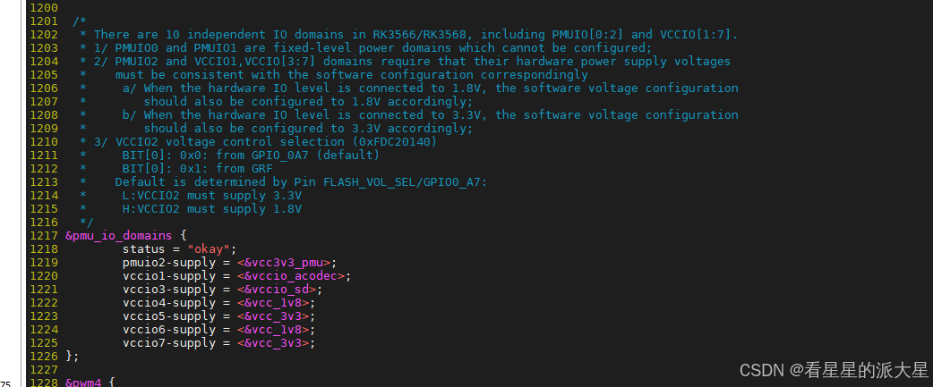
来看看这段解释:
1201 /*
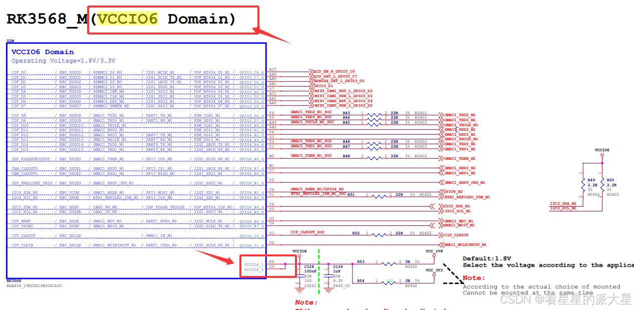
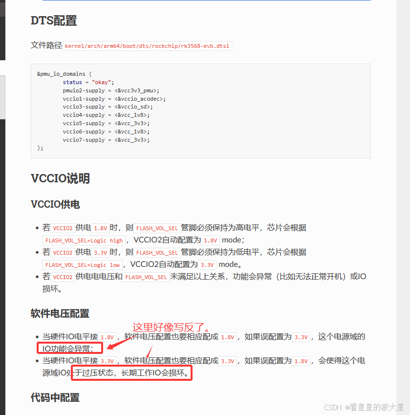
1202 * There are 10 independent IO domains in RK3566/RK3568, including PMUIO[0:2] and VCCIO[1:7].
1203 * 1/ PMUIO0 and PMUIO1 are fixed-level power domains which cannot be configured;
1204 * 2/ PMUIO2 and VCCIO1,VCCIO[3:7] domains require that their hardware power supply voltages
1205 * must be consistent with the software configuration correspondingly
1206 * a/ When the hardware IO level is connected to 1.8V, the software voltage configuration
1207 * should also be configured to 1.8V accordingly;
1208 * b/ When the hardware IO level is connected to 3.3V, the software voltage configuration
1209 * should also be configured to 3.3V accordingly;
1210 * 3/ VCCIO2 voltage control selection (0xFDC20140)
1211 * BIT[0]: 0x0: from GPIO_0A7 (default)
1212 * BIT[0]: 0x1: from GRF
1213 * Default is determined by Pin FLASH_VOL_SEL/GPIO0_A7:
1214 * L:VCCIO2 must supply 3.3V
1215 * H:VCCIO2 must supply 1.8V
1216 */
所谓的电源域是不是这个意思:
电源域只是 针对cpu 来说的,
cpu 的一组的io口 能够承受多大的电压,是需要配置寄存器的,就相当于 配置stm32的 gpio 的寄存器一样。
至于 rk806这个 电源芯片输出多大的电压,那就是 i2c 的配置的问题了,跟电源域就没有关系了。
---------------------------------------------------------------------------------------
上面 七七八八, 写了很多, 但是 都是猜的, 因为毕竟 硬件不是我设计的,驱动也不是我写的。
下载我又有了点 新的 理解。
首先是 先来一张图。
这张图是 , 关于 3568 的硬件上的 电源的连接。
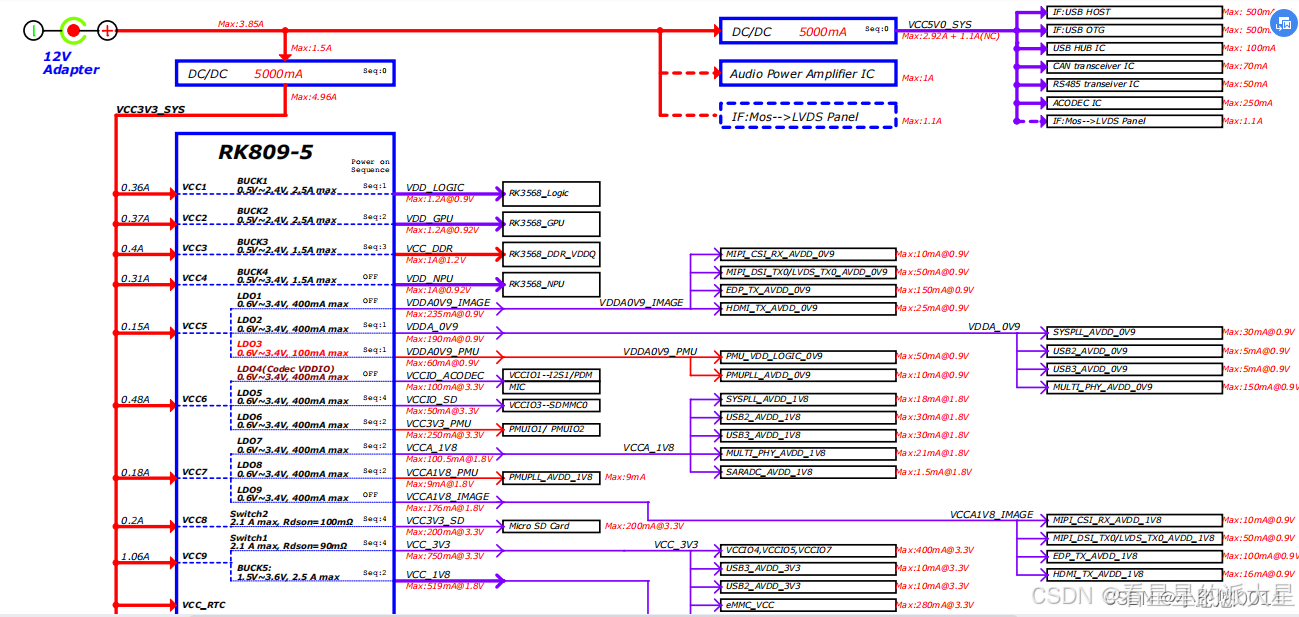
好了,硬件上 准备好了,
还需要 在 软件上 进行配置才行。
那么就在设备树中进行配置吧。
我就 拿这个 做示范吧。这是从 oopenharmony4.0 的 3568 的 hihope 的 内核中 的设备树中 拷贝出来的。
1563 /**
1 * Model: TB-RK3568X
2 * -----------------------------------------------------------
3 * There are 10 independent IO domains in RK3566/RK3568, including PMUIO[0:2] and VCCIO[1:7].
4 * 1/ PMUIO0 and PMUIO1 are fixed-level power domains which cannot be configured;
5 * 2/ PMUIO2 and VCCIO1,VCCIO[3:7] domains require that their hardware power supply voltages
6 * must be consistent with the software configuration correspondingly
7 * a/ When the hardware IO level is connected to 1.8V, the software voltage configuration
8 * should also be configured to 1.8V accordingly;
9 * b/ When the hardware IO level is connected to 3.3V, the software voltage configuration
10 * should also be configured to 3.3V accordingly;
11 * 3/ VCCIO2 voltage control selection (0xFDC20140)
12 * BIT[0]: 0x0: from GPIO_0A7 (default)
13 * BIT[0]: 0x1: from GRF
14 * Default is determined by Pin FLASH_VOL_SEL/GPIO0_A7:
15 * L:VCCIO2 must supply 3.3V
16 * H:VCCIO2 must supply 1.8V
17 * | supply | domain | net | source | voltage |
18 * -----------------------------------------------------------
19 * | pmuio1-supply | PMUIO1 | vcc3v3_pmu | LDO6 | 3.3V |
20 * | pmuio2-supply | PMUIO2 | vcc3v3_pmu | LDO6 | 3.3V |
21 * | vccio1-supply | VCCIO1 | vccio_acodec | LDO4 | 1.8V |
22 * | vccio2-supply | VCCIO2 | vccio_flash | vcc_1v8 | 1.8V |
23 * | vccio3-supply | VCCIO3 | vccio_sd | LDO5 | 3.3V |
24 * | vccio4-supply | VCCIO4 | vcc_1v8 | DCDC5 | 1.8V |
25 * | vccio5-supply | VCCIO5 | vcc_3v3 | SWITCH1 | 3.3V |
26 * | vccio6-supply | VCCIO6 | vcc_1v8 | DCDC5 | 1.8V |
27 * | vccio7-supply | VCCIO7 | vcc_3v3 | SWITCH1 | 3.3V |
28 * -----------------------------------------------------------
29 */
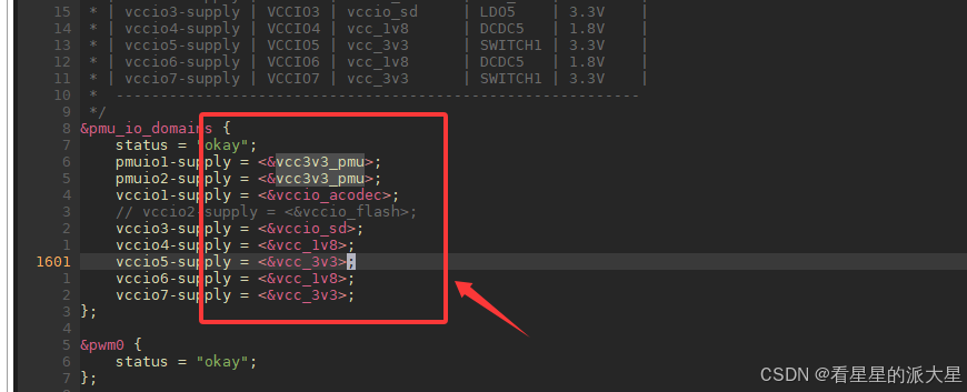
30 &pmu_io_domains {
31 status = "okay";
32 pmuio1-supply = <&vcc3v3_pmu>;
33 pmuio2-supply = <&vcc3v3_pmu>;
34 vccio1-supply = <&vccio_acodec>;
35 // vccio2-supply = <&vccio_flash>;
36 vccio3-supply = <&vccio_sd>;
37 vccio4-supply = <&vcc_1v8>;
38 vccio5-supply = <&vcc_3v3>;
39 vccio6-supply = <&vcc_1v8>;
40 vccio7-supply = <&vcc_3v3>;
41 };
注意: 首先我要搞明白, 设备树中的左边 的 字段 对应的是什么, 右边 对应的字段对应的是什么,
pmuio1
pmuio2
vccio3
....
这些对应的是 原理图中的硬件。 这些图 肯定也是 瑞芯微画的。
那么 右边呢?
举个例子,
vcc3v3_pmu
     1             vcc3v3_pmu: LDO_REG6 {
  1315                 regulator-always-on;
     1                 regulator-boot-on;
     2                 regulator-min-microvolt = <3300000>;
     3                 regulator-max-microvolt = <3300000>;
     4                 regulator-name = "vcc3v3_pmu";
     5                 regulator-state-mem {
     6                     regulator-on-in-suspend;
     7                     regulator-suspend-microvolt = <3300000>;
     8                 };
     9             };
看到了吧, 这是 一个配置的节点。
也就是说 我把 pmuio1-supply = <&vcc3v3_pmu>; 这句话写出来之后, 它肯定会去配置寄存器的。配置的应该是 cpu 的寄存器。
具体做么做的不去理解。 这是 软件上的配置。
再来看看这个 ,这就更清晰了。
    41         regulators {
    40             vdd_logic: DCDC_REG1 {
    39                 regulator-always-on;
    38                 regulator-boot-on;
    37                 regulator-min-microvolt = <500000>;
    36                 regulator-max-microvolt = <1350000>;
    35                 regulator-init-microvolt = <900000>;
    34                 regulator-ramp-delay = <6001>;
    33                 regulator-initial-mode = <0x2>;
    32                 regulator-name = "vdd_logic";
    31                 regulator-state-mem {
    30                     regulator-off-in-suspend;
    29                 };
    28             };
    27
    26             vdd_gpu: DCDC_REG2 {
    25                 regulator-always-on;
    24                 regulator-boot-on;
    23                 regulator-min-microvolt = <500000>;
    22                 regulator-max-microvolt = <1350000>;
    21                 regulator-init-microvolt = <900000>;
    20                 regulator-ramp-delay = <6001>;
    19                 regulator-initial-mode = <0x2>;
    18                 regulator-name = "vdd_gpu";
    17                 regulator-state-mem {
    16                     regulator-off-in-suspend;
    15                 };
    14             };
    13
    12             vcc_ddr: DCDC_REG3 {
    11                 regulator-always-on;
    10                 regulator-boot-on;
     9                 regulator-initial-mode = <0x2>;
     8                 regulator-name = "vcc_ddr";
     7                 regulator-state-mem {
     6                     regulator-on-in-suspend;
     5                 };
     4             };
     3
     2             vdd_npu: DCDC_REG4 {
     1                 regulator-always-on;
  1246                 regulator-boot-on;
     1                 regulator-min-microvolt = <500000>;
     2                 regulator-max-microvolt = <1350000>;
     3                 regulator-init-microvolt = <900000>;
     4                 regulator-ramp-delay = <6001>;
     5                 regulator-initial-mode = <0x2>;
     6                 regulator-name = "vdd_npu";
     7                 regulator-state-mem {
     8                     regulator-off-in-suspend;
     9                 };
    10             };

    44
    43             vdda0v9_image: LDO_REG1 {
    42                 regulator-boot-on;
    41                 regulator-always-on;
    40                 regulator-min-microvolt = <900000>;
    39                 regulator-max-microvolt = <900000>;
    38                 regulator-name = "vdda0v9_image";
    37                 regulator-state-mem {
    36                     regulator-off-in-suspend;
    35                 };
    34             };
    33
    32             vdda_0v9: LDO_REG2 {
    31                 regulator-always-on;
    30                 regulator-boot-on;
    29                 regulator-min-microvolt = <900000>;
    28                 regulator-max-microvolt = <900000>;
    27                 regulator-name = "vdda_0v9";
    26                 regulator-state-mem {
    25                     regulator-off-in-suspend;
    24                 };
    23             };
    22
    21             vdda0v9_pmu: LDO_REG3 {
    20                 regulator-always-on;
    19                 regulator-boot-on;
    18                 regulator-min-microvolt = <900000>;
    17                 regulator-max-microvolt = <900000>;
    16                 regulator-name = "vdda0v9_pmu";
    15                 regulator-state-mem {
    14                     regulator-on-in-suspend;
    13                     regulator-suspend-microvolt = <900000>;
    12                 };
    11             };
    10
     9             vccio_acodec: LDO_REG4 {
     8                 regulator-always-on;
     7                 regulator-boot-on;
     6                 regulator-min-microvolt = <1800000>;
     5                 regulator-max-microvolt = <1800000>;
     4                 regulator-name = "vccio_acodec";
     3                 regulator-state-mem {
     2                     regulator-off-in-suspend;
     1                 };
  1301             };
     1
     2             vccio_sd: LDO_REG5 {
     3                 regulator-always-on;
     4                 regulator-boot-on;
     5                 regulator-min-microvolt = <1800000>;
     6                 regulator-max-microvolt = <3300000>;
     7                 regulator-name = "vccio_sd";
     8                 regulator-state-mem {
     9                     regulator-off-in-suspend;
    10                 };

    42             vcc3v3_pmu: LDO_REG6 {
    41                 regulator-always-on;
    40                 regulator-boot-on;
    39                 regulator-min-microvolt = <3300000>;
    38                 regulator-max-microvolt = <3300000>;
    37                 regulator-name = "vcc3v3_pmu";
    36                 regulator-state-mem {
    35                     regulator-on-in-suspend;
    34                     regulator-suspend-microvolt = <3300000>;
    33                 };
    32             };
    31
    30             vcca_1v8: LDO_REG7 {
    29                 regulator-always-on;
    28                 regulator-boot-on;
    27                 regulator-min-microvolt = <1800000>;
    26                 regulator-max-microvolt = <1800000>;
    25                 regulator-name = "vcca_1v8";
    24                 regulator-state-mem {
    23                     regulator-off-in-suspend;
    22                 };
    21             };
    20
    19             vcca1v8_pmu: LDO_REG8 {
    18                 regulator-always-on;
    17                 regulator-boot-on;
    16                 regulator-min-microvolt = <1800000>;
    15                 regulator-max-microvolt = <1800000>;
    14                 regulator-name = "vcca1v8_pmu";
    13                 regulator-state-mem {
    12                     regulator-on-in-suspend;
    11                     regulator-suspend-microvolt = <1800000>;
    10                 };
     9             };
     8
     7             vcca1v8_image: LDO_REG9 {
     6                 regulator-always-on;
     5                 regulator-boot-on;
     4                 regulator-min-microvolt = <1800000>;
     3                 regulator-max-microvolt = <1800000>;
     2                 regulator-name = "vcca1v8_image";
     1                 regulator-state-mem {
  1356                     regulator-off-in-suspend;
     1                 };
     2             };
    37             vcc_1v8: DCDC_REG5 {
    36                 regulator-always-on;
    35                 regulator-boot-on;
    34                 regulator-min-microvolt = <1800000>;
    33                 regulator-max-microvolt = <1800000>;
    32                 regulator-name = "vcc_1v8";
    31                 regulator-state-mem {
    30                     regulator-off-in-suspend;
    29                 };
    28             };
    27
    26             vcc_3v3: SWITCH_REG1 {
    25                 regulator-always-on;
    24                 regulator-boot-on;
    23                 regulator-name = "vcc_3v3";
    22                 regulator-state-mem {
    21                     regulator-off-in-suspend;
    20                 };
    19             };
    18
    17             vcc3v3_sd: SWITCH_REG2 {
    16                 regulator-always-on;
    15                 regulator-boot-on;
    14                 regulator-name = "vcc3v3_sd";
    13                 regulator-state-mem {
    12                     regulator-off-in-suspend;
    11                 };
    10             };
     9         };
这里已经明确的 指出了。
dcdc1
dcdc2
.......
switch_reg2 .
这里完全是 跟硬件对应的。
总结:
1 我觉的左边的,右边的字段 都是有特定含义的, 右边的很明确了,就是在设置 PMU的寄存器。 左边的有可能是 在 配置 cpu 的寄存器。
2 我觉得 右边的 LDO_REG1, LDO_REG2 应该是 重复的,因为在寄存器上他们 应该是一样的。
3 也就是 右边是在配置 rk809 , 左边是在配置 cpu
总是听人说 , 硬件的配置 与 软件设备树的 配置要一致,否则要 烧cpu .
来看一段截图。
那么什么是硬件 配置呢?
举例:
我就拿第一个 来举例。
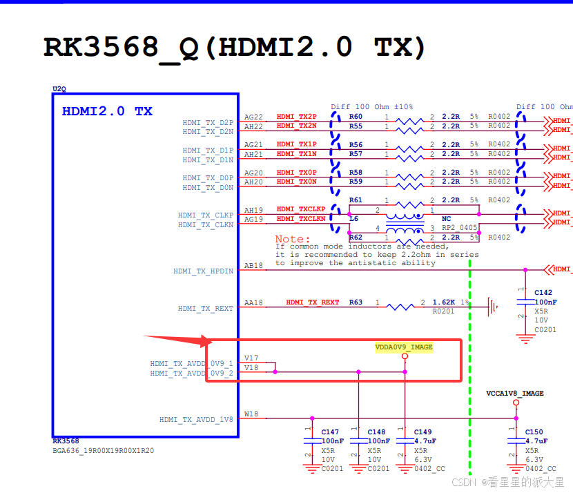
这就是 实际上的 硬件的连接了。
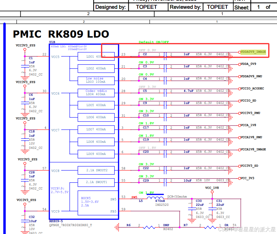
HDMI 使用的是 VDDA0V9_IMAGE 这个脚来供电。
那么在这里 我配置 一个 vcc3.3 的 节点可以吗?(虽然实际上 pmu 这里并没有 管这个脚)
实际软件设置上是可以的,
但是 这就出现了 不一致。
总结: 一般 用着用着 就出现烧 cpu 的情况的,都可以 从 这里 去考虑下。
再来看一下 其他的 点。
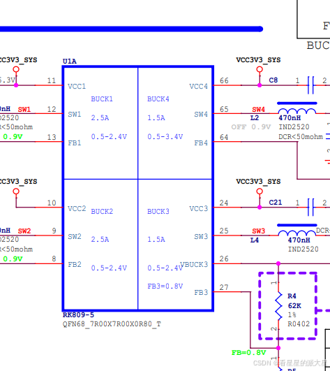
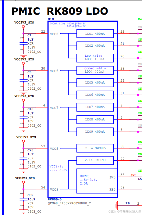
我们可以看到 ,在软件上 能够控制的 有 5组 buck ,4组 ldo .
实际上 它每设置 一组寄存器的值, 控制的 是 3个ldo , 这也符合 逻辑。
好了, 总结完毕。
-----------------------------------------------------------------------------------------


 2766
2766

 被折叠的 条评论
为什么被折叠?
被折叠的 条评论
为什么被折叠?
 到【灌水乐园】发言


