


 本文介绍了一种使用Vivado中的VIO(Virtual Input/Output)IP核来控制DDS(Direct Digital Synthesizer)IP核的方法,通过模拟按键控制频率控制字,实现不同频率正弦波的生成。
vivado VIO IP的用法
0 程序功能
通过VIO模拟按键来控制DDS的频率控制字,从而得到不同频率的正弦波。
程序结构
必须要通过ILA才能模拟VIO,testbench不能模拟VIO。
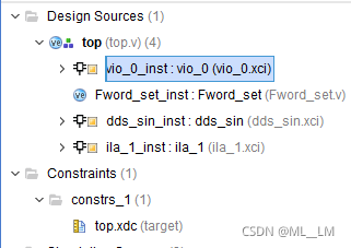
1 IP核的例化
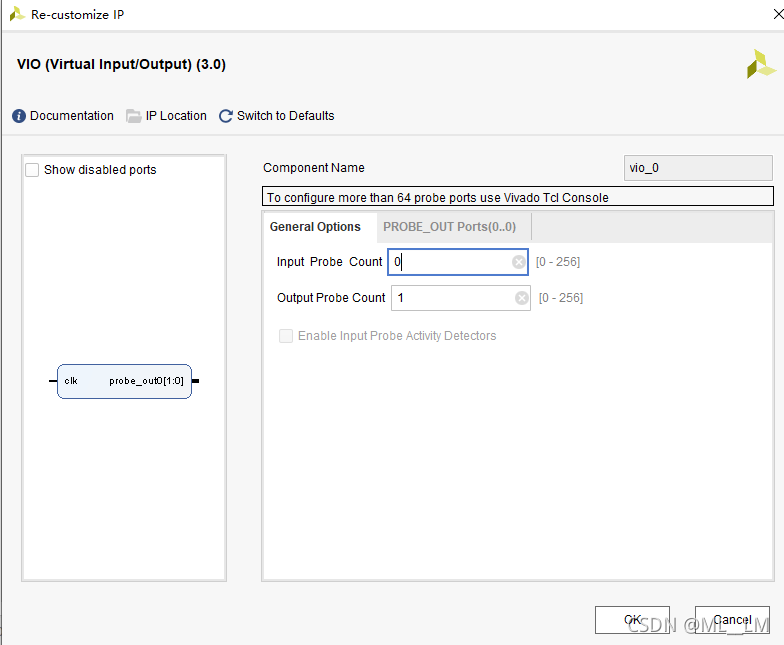
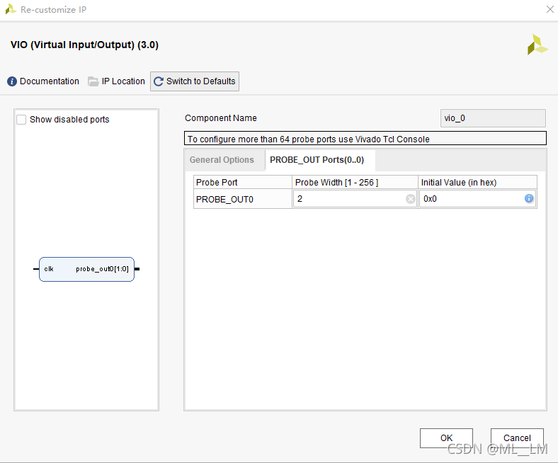
1.1 VIO IP的例化
vio_0 your_instance_name (
  .clk(clk),                // input wire clk
  .probe_out0(probe_out0)  // output wire [1 : 0] probe_out0
);
1.2 DDS IP
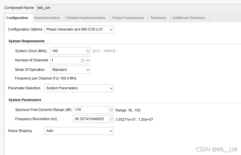
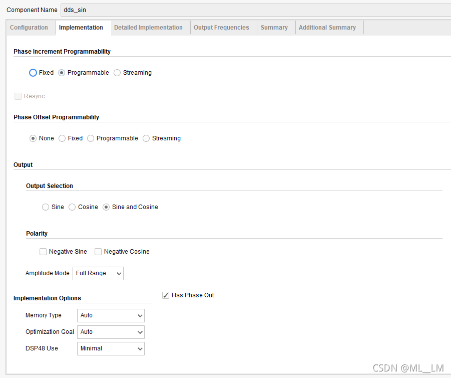
dds_sin your_instance_name (
  .aclk(aclk),                                  // input wire aclk
  .s_axis_config_tvalid(s_axis_config_tvalid),  // input wire s_axis_config_tvalid
  .s_axis_config_tdata(s_axis_config_tdata),    // input wire [23 : 0] s_axis_config_tdata
  .m_axis_data_tvalid(m_axis_data_tvalid),      // output wire m_axis_data_tvalid
  .m_axis_data_tdata(m_axis_data_tdata),        // output wire [47 : 0] m_axis_data_tdata
  .m_axis_phase_tvalid(m_axis_phase_tvalid),    // output wire m_axis_phase_tvalid
  .m_axis_phase_tdata(m_axis_phase_tdata)      // output wire [23 : 0] m_axis_phase_tdata
);
2 程序
2.1 程序结构
2.2 顶层模块
`timescale 1ns / 1ps


module top(
    input           sys_clk         ,//系统时钟  50MHz  T=20ns
    input           rst_n           //系统复位
    );


// -----------0、VIO按键控制频率控制字(key_PINC)
 wire [1:0] key_PINC;
 vio_0 vio_0_inst (
      .clk(sys_clk),                // input wire clk
      .probe_out0(key_PINC)  // output wire [1 : 0] probe_out0
    );


//---------------1、信号频率控制模块--------------//
wire  [23:0]   Fword ;  //频率字
Fword_set Fword_set_inst(
        //input
        .clk        (sys_clk            ),
        .rst_n      (rst_n              ),
        .key_PINC   (key_PINC           ),
        //output
        .Fword      (Fword              )
        );


//---------------2、DDS模块--------------//
//input
wire [0:0]   fre_ctrl_word_en  ;

//output
wire [0:0]   m_axis_data_tvalid    ;
wire [47:0]  m_axis_data_tdata     ;
wire [0:0]   m_axis_phase_tvalid   ;
wire [23:0]  m_axis_phase_tdata    ;

assign fre_ctrl_word_en=1'b1;

//例化DDS IP
dds_sin dds_sin_inst (
  .aclk                 (sys_clk                ),    // input wire aclk
  .s_axis_config_tvalid (fre_ctrl_word_en       ),    // input wire s_axis_config_tvalid
  .s_axis_config_tdata  (Fword                  ),    // input wire [23: 0] s_axis_config_tdata

  .m_axis_data_tvalid   (m_axis_data_tvalid     ),    // output wire m_axis_data_tvalid
  .m_axis_data_tdata    (m_axis_data_tdata      ),    // output wire [47 : 0] m_axis_data_tdata
  .m_axis_phase_tvalid  (m_axis_phase_tvalid    ),    // output wire m_axis_phase_tvalid
  .m_axis_phase_tdata   (m_axis_phase_tdata     )     // output wire [23 : 0] m_axis_phase_tdata
);


 ila_1 ila_1_inst (
	.clk(sys_clk), // input wire clk


	.probe0(key_PINC), // input wire [1:0]  probe0
	.probe1(Fword), // input wire [23:0]  probe1
	.probe2(m_axis_data_tdata) // input wire [47:0]  probe2
);


endmodule
2.3 Fword_set模块
`timescale 1ns / 1ps
//
// 通过按键来选择对应的频率控制字,进而选择对应的信号频率
//
module Fword_set(
input clk ,
input rst_n ,
input [1:0] key_PINC ,
output reg [23:0] Fword
);
//always@(posedge clk or negedge rst_n)
//begin
// if(!rst_n)
// key_sel <= 4'd0;
// else
// key_sel <= key_sel;
//end
// The output frequency(f_out ) , of the DDS waveform is a function of the system clock frequency(f_clk ) .
// the phase width, that is, number of bits (B ) in the phase accumulator
// and the phase increment value (deta_theta) .
// The output frequency in Hertz is defined by:f_out=f_clk*deta_theta/(2^B)
// fre_ctrl_word是如何确定的?
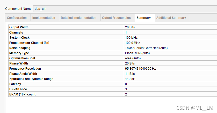
// 根据IP核的summery, phase width=20bits Frequency per channel=100MHz
// 输出频率的计算公式f_out=f_clk*deta_theta/(2^B)=100M* 104857/(2^20 )= 10M
always@(*)
begin
case(key_PINC)
0: Fword <= 'h28f5; //1Mhz 10485 每次相位增加的值 deta_theta
1: Fword <= 'h51eb; //2Mhz 20971
2: Fword <= 'ha3d7; //4Mhz 41943
3: Fword <= 'h19999; //10Mhz 104857
endcase
end
endmodule
2.4 约束文件
set_property PACKAGE_PIN U18 [get_ports sys_clk]
set_property IOSTANDARD LVCMOS33 [get_ports sys_clk]


set_property PACKAGE_PIN J16 [get_ports rst_n]
set_property IOSTANDARD LVCMOS33 [get_ports rst_n]


#时序约束
create_clock -period 20.000 -name sys_clk -waveform {0.000 10.000} [get_ports sys_clk]
3 结果
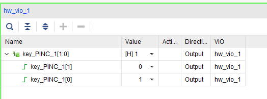
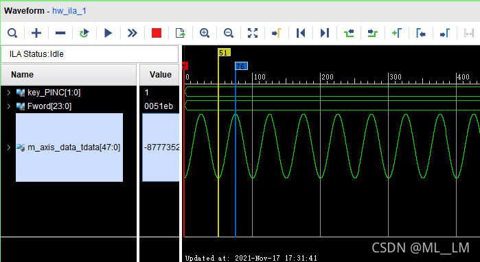
key_PINC=0(2’b01)
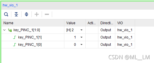
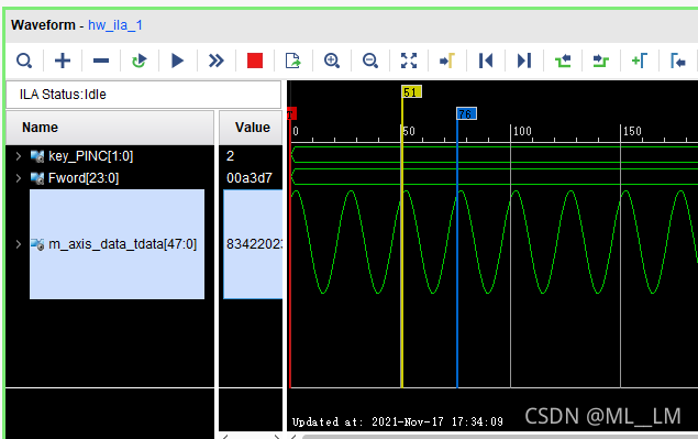
key_PINC=2(2’b10)


 2万+
2万+

 被折叠的 条评论
为什么被折叠?
被折叠的 条评论
为什么被折叠?
 到【灌水乐园】发言


