IP核之PLL

一.IP核简介

  • IP,知识产权。其可分为三种:软核,固核,硬核

1.软核

  • 它是用硬件描述语言(HDL)设计的独立功能的电路模块。它以综合源代码的形式交付给用户,其优点是源代码灵活,在功能一级可以重新配置,可以灵活选择目标制造工艺。灵活性高、可移植性强,允许用户自配置。其缺点是对电路功能模块的预测性较差,在后续设计中存在发生错误的可能性,有一定的设计风险。并且IP软核的知识产权保护难度较大。

2.固核

  • 它的设计程度介于IP软核和IP硬核之间,它除了完成IP软核所有的设计外,还完成了门级电路综合和时序仿真等设计环节。它的灵活性和成功率介于IP软核和IP硬核之间,是一种折中的类型。和IP软核相比,IP固核的设计灵活性稍差,但在可靠性上有较大提高。

3.硬核

  • 它提供了电路设计最后阶段掩模级的电路模块。它以最终完成的布局布线网表形式提供给用户。IP硬核既具有结果的可预见性,也可以针对特定工艺或特定IP提供商进行功耗和尺寸的优化。它的最大优点是确保性能,如速度、功耗等达到预期效果。然而,IP硬核与制造工艺相关,难以转移到新的工艺或者集成到新的结构中去,是不可以重新配置的。IP硬核不许修改的特点使其复用有一定的困难,因此只能用于某些特定应用,使用范围较窄。但IP硬核的知识产权保护最为方便。

二.PLL核简介

  • PLL(锁相环),其功能有:时钟分频,时钟倍频,调节相位,调节占空比。PLL核就是一种硬核。

  • PLL原理是一个反馈电路,原理如下图:
    在这里插入图片描述

  • 我们使用的EP4CEF17C8芯片有两个PLL,每个PLL可以有5路输出

  • 注意:!!!FPGA内部生成的信号不能控制PLL!!!

三.PLL IP核配置

  • 新建工程后在Quartus右侧IP Catalog中输入PLL,选择ALTPLL
    在这里插入图片描述

  • 选择路径,为文件命名,选择verilog语言
    在这里插入图片描述

  • 配置速度等级和时钟频率
    在这里插入图片描述

  • Next后配置如下
    在这里插入图片描述

  • Next后保持默认
    在这里插入图片描述

  • Next后保持默认
    在这里插入图片描述

  • Next后保持默认
    在这里插入图片描述

  • 配置需要的输出信号
    在这里插入图片描述

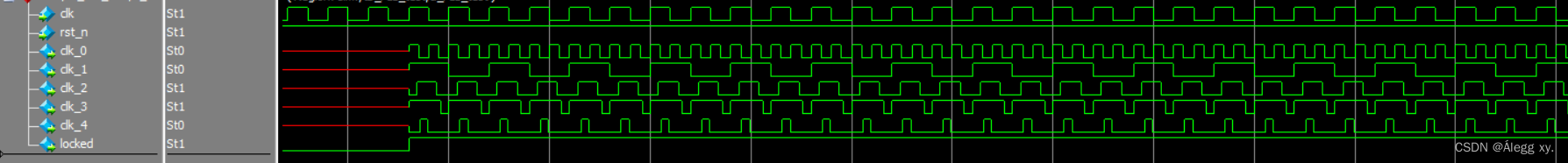
  • 按自己的需求配置,为了考察PLL的各个功能,我配置的输出信号如下

输出信号功能
c0输入时钟的二倍频
c1输入时钟的二分频
c2相位偏移71.25
c3占空比80%
c4相位偏移101.25,占空比为20%
  • EDA配置保持默认
    在这里插入图片描述

  • 选择需要得到的文件
    在这里插入图片描述

三.PLL IP核的调用

  • 刚刚选择得到的文件中选中了IP_PLL_inst.v文件,这个文件就是例化模块,在工程文件夹下的rtl子文件夹下建立一个.v文件,可以直接调用该例化模块的代码
  • PLL_test.v
/**************************************功能介绍***********************************
Date	: 
Author	: Alegg xy.
Version	: 
Description: 
*********************************************************************************/
    
//---------<模块及端口声名>------------------------------------------------------
module PLL_test( 
    input				clk		,
    input				rst_n	,
    output				clk_0	,
    output              clk_1   ,
    output              clk_2   ,
    output              clk_3   ,
    output              clk_4   ,
    output              locked  
);								 
//---------<参数定义>--------------------------------------------------------- 
    
//---------<内部信号定义>-----------------------------------------------------
    IP_PLL	IP_PLL_inst (
	.areset ( !rst_n ),
	.inclk0 ( clk ),
	.c0 ( clk_0 ),
	.c1 ( clk_1 ),
	.c2 ( clk_2 ),
	.c3 ( clk_3 ),
	.c4 ( clk_4 ),
	.locked ( locked )
	);
 
endmodule
  • 注意:PLL IP核异步复位高有效,系统复位低有效。因此例化时需要取反
    在这里插入图片描述

四.PLL IP核的仿真

  • tb_PLL_test.v(仿真)
`timescale 1ns/1ns
    
module tb_PLL_test();

//激励信号定义 
    reg				tb_clk  	;
    reg				tb_rst_n	;

//输出信号定义	 
    wire			tb_clk_0	;
    wire			tb_clk_1    ;
    wire            tb_clk_2    ;
    wire            tb_clk_3    ;
    wire            tb_clk_4    ;
    wire            tb_locked   ;

//时钟周期参数定义	
    parameter		CLOCK_CYCLE = 20;   

//模块例化
    PLL_test u_PLL_test(	
        .clk		(tb_clk),
        .rst_n	    (tb_rst_n),
        .clk_0	    (tb_clk_0),
        .clk_1      (tb_clk_1),
        .clk_2      (tb_clk_2),
        .clk_3      (tb_clk_3),
        .clk_4      (tb_clk_4),
        .locked     (tb_locked)
    );

//产生时钟
    initial 		tb_clk = 1'b0;
    always #(CLOCK_CYCLE/2) tb_clk = ~tb_clk;

//产生激励
    initial  begin 
        tb_rst_n = 1'b1;
        #(CLOCK_CYCLE*2);
        tb_rst_n = 1'b0;
        #(CLOCK_CYCLE*20);
        tb_rst_n = 1'b1;
        #(CLOCK_CYCLE*100);
        $stop;


    end

endmodule 
  • 仿真效果
    在这里插入图片描述
### Vivado IP Core PLL Configuration and Usage In the context of configuring Phase-Locked Loop (PLL) cores within Xilinx's Vivado Design Suite, users can leverage the comprehensive IP catalog available through the tool. From this catalog, one may explore various IPs including those pertinent to clock management such as the PLLs [^2]. The PLL is instrumental in generating multiple output clocks from a single input reference clock with options for frequency multiplication or division. To configure an IP core like the PLL: Navigate to the **IP Catalog** by selecting `Window` -> `IP Catalog`. Within this interface, search for "Clocking Wizard" which often serves as the means to instantiate PLL configurations. Upon opening the Clocking Wizard GUI, parameters specific to the design requirements are set up here. These include defining primary input/output characteristics alongside advanced settings that cater to jitter performance, duty cycle adjustment among others [^1]. After setting these properties according to project needs, proceed with generation and integration into the broader system design flow. Once generated, incorporating the configured PLL instance involves adding it to your block diagram via drag-and-drop functionality provided within Vivado’s environment [^3]. For detailed guidance on each configurable parameter along with best practices concerning implementation strategies, refer to documentation associated directly with the selected IP version accessible under its respective sections found inside the IP catalog . ```python # Example Python snippet demonstrating how you might interact programmatically with Vivado Tcl commands related to creating a new PLL. set clk_wiz_name "clk_wiz_0" create_ip -vendor xilinx.com -library ip -module_name $clk_wiz_name set_property -dict [list CONFIG.PRIM_IN_FREQ.VALUE_SRC USER \ CONFIG.CLKOUT1_REQUESTED_OUT_FREQ {100} \ CONFIG.MMCM_DIVCLK_DIVIDE {1}] [get_ips ${clk_wiz_name}] generate_target all [get_files ./${clk_wiz_name}.xci] ```
评论
添加红包

请填写红包祝福语或标题

红包个数最小为10个

红包金额最低5元

当前余额3.43前往充值 >
需支付:10.00
成就一亿技术人!
领取后你会自动成为博主和红包主的粉丝 规则
hope_wisdom
发出的红包
实付
使用余额支付
点击重新获取
扫码支付
钱包余额 0

抵扣说明:

1.余额是钱包充值的虚拟货币,按照1:1的比例进行支付金额的抵扣。
2.余额无法直接购买下载,可以购买VIP、付费专栏及课程。

余额充值