


一、实验目的
1. 进一步学习FPGA开发流程和使用开发工具
2. 熟悉HDL语言进行组合逻辑电路设计
二、实验设备
1、 计算机
2、 实验板
三、实验要求:
1、在PC机上完成仿真,对结果进行分析;
2、完成下载,在实验板上进行验证。
四、实验内容
(一)任务一:编码器设计
1、设计原理
八个拨码开关代表0~7,用二进制对其编码。真值表如下:

2、给出设计源文件
`timescale 1ns / 1ps
module encoder_8_3(
input[7:0]a,
output reg[2:0]b
);
always@(a)
case(a)
8'b00000001 : b<=3'b000;//输入00000001,输出000
8'b00000010 : b<=3'b001;//输入00000010,输出001
8'b00000100 : b<=3'b010;//输入00000100,输出010
8'b00001000 : b<=3'b011;//输入00001000,输出011
8'b00010000 : b<=3'b100;//输入00010000,输出100
8'b00100000 : b<=3'b101;//输入00100000,输出101
8'b01000000 : b<=3'b110;//输入01000000,输出110
8'b10000000 : b<=3'b111;//输入10000000,输出111
default : b<= 3'b000;
endcase
endmodule
3、仿真测试文件
`timescale 1ns / 1ps
module encoder8_3_sim(
input[7:0]inPut,
output[2:0]outPut
);
reg[7:0]a;//创建中间变量
initial
begin
a=8'b00000001;#100;
a=8'b00000010;#100;
a=8'b00000100;#100;
a=8'b00001000;#100;
a=8'b00010000;#100;
a=8'b00100000;#100;
a=8'b01000000;#100;
a=8'b10000000;#100;
end
assign inPut=a;
encoder_8_3 u1(inPut,outPut);//调用主函数
endmodule
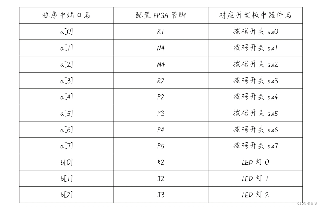
实验板为


 1664
1664


 被折叠的 条评论
为什么被折叠?
被折叠的 条评论
为什么被折叠?
 到【灌水乐园】发言


