


Why CMOS?
- Output of all CMOS cells will be very close to rail-rail (may not be in case of Pass Transistor)
- With constant input to any cell, power dissipation is only due to leakage currents. Power dissipation increase if activity factor is more (Short circuit current + charging & discharging of load)
- Analog, RF & Memory can be integrated in single chip in case of CMOS process
- High impedance inputs with voltage as a trigger. Very little current passes through the input.
- CMOS provides full swing of VDD through PMOS & GND through NMOS
- Temperature stability is more (-60 C – 130 C)
- Noise immunity is high (switching happens close to VDD/2) (Higher noise margins)
Before deep-diving into CMOS basic, let’s discuss & understand basis of RC. Thorough understating of RC is very much required in VLSI domain and it helps a lot in complex analyses. I would say, if we understand all basic concepts very well, we can analyze & solve any problem very easily.
RC (Why RC is important?)
Definitely we cannot build a complete & accurate model of CMOS using R & C. Hundreds of parameters are required to model a CMOS accurately (LEVEL 54 BSIM4.0 Model). But for a digital design/PD engineer, an abstract level understanding of MOSFET will definitely help in understanding & analyzing complex circuits & issues. So I would recommend you to understand the RC model of CMOS thoroughly.
Resistance effect (Width of MOSFET)
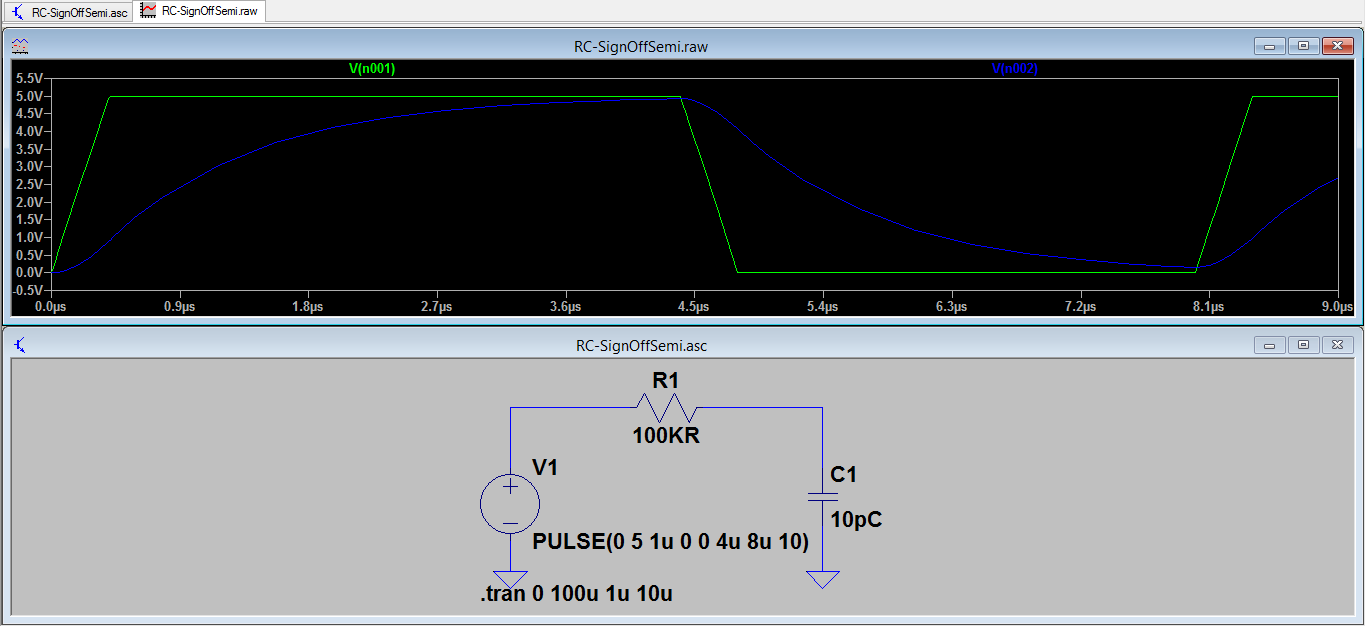
Consider RC circuit with R = 100k-Ohm & C = 10pF. Current I, is inversely proportional to Resistance R. If R is high, then current will be less & hence more time is required to charge the load capacitor. Refer below circuit, V(n001) [green] is supply & V(n002) [blue] is voltage across capacitor. Observe the voltage graph across capacitor, charging time is high because of high resistance.
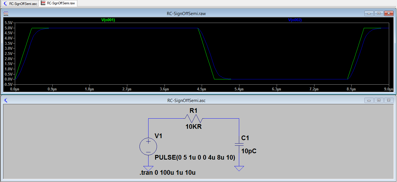
Lets reduce Resistance R to 10k Ohm. As R is reduced, I increases & hence charging / dis-charging time of Capacitor C are reduced. Refer below circuit.
Now lets extend this understanding to MOSFET. Drain current in MOSFET, Id = u*Cox*W*sq(Vgs-Vt) / 2L & On-resistance of MOSFET depends on W(width) & L(Length). Higher the value of W, lower the resistance & current carrying capability of MOSFET is more.
“Hence increasing the width of MOSFET reduce the charging & dis-charging time of the load capacitor (charging & dis-charging time are nothing but rise & fall time)” . In digital circuit implementation (Synthesis & PnR), width can varied by using different drive strength cells. (like BUF-D1 (w=1u), BUF-D2 (w=2u), BUF-D3 (w=3u)…)”
“Current through MOSFET can be increased by increasing width of the device & hence reducing the rise time / fall time (Charge / Di-charge time of load capacitor)”
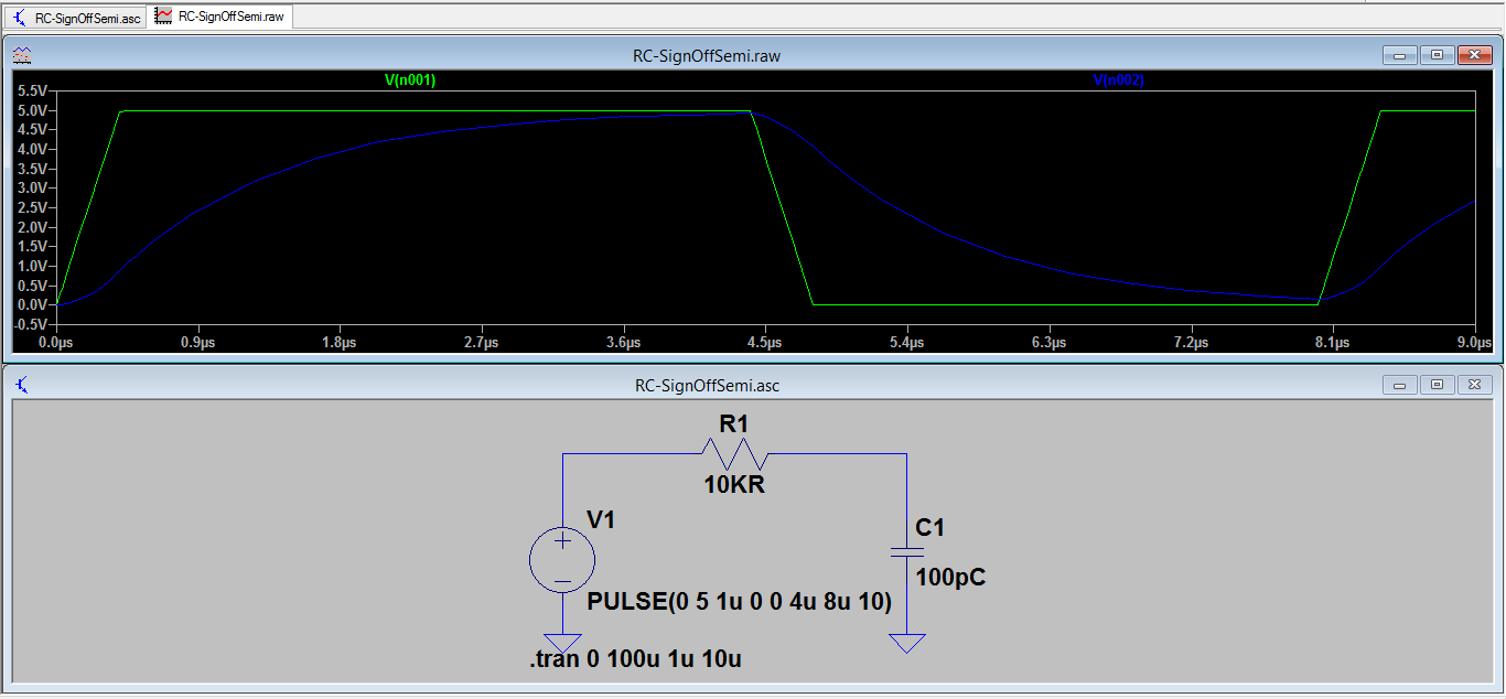
Capacitance effect (Load Cap / Fan-Out)
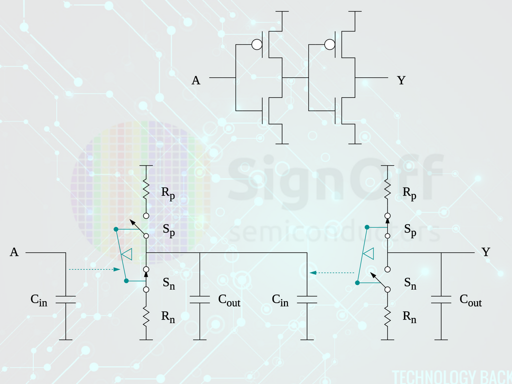
RC Model of a Buffer
CMOS Basics
Why PMOS is slower than NMOS?
Most of the answers would stop at “Mobility of hole is lesser than mobility of electrons in semiconductor”. Obviously next question would be “Why?”
To understand this concept, let’s go back to basics of energy band diagrams.
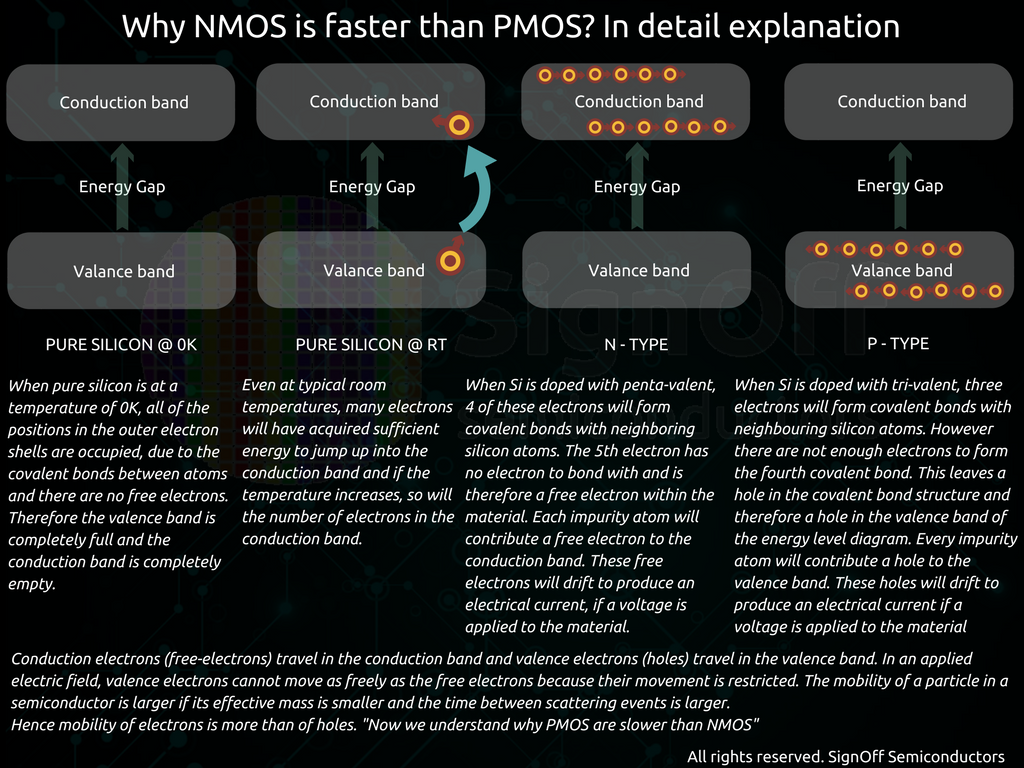
Conduction electrons (free-electrons) travel in the conduction band and valence electrons (holes) travel in the valence band. In an applied electric field, valence electrons cannot move as freely as the free electrons because their movement is restricted. The mobility of a particle in a semiconductor is larger if its effective mass is smaller and the time between scattering events is larger.
Hence mobility of electrons is more than of holes. “Now we understand why PMOS are slower than NMOS”
In short, ‘Hole’s movement in valence band requires more energy (voltage) compared to free electron in conduction band’
Because of this mobility mis-match, beta ratio comes into picture while design standard logic cells. And we also require special cells for clock network, whose rise & fall time are very well balanced. Why clock cells need this balance? We will discuss on this in CTS training session.
PROCESS OVERVIEW
Most of the semicon giants do lot of research in process technology. Increasing need of ultra low power, high performance, small form factor & low cost ICs is making Fabs/Companies to put more money on the research. Traditional planar bulk process has many issues with further scaling (like leakage & short channel effects). As of now there are two most popular solutions for this problem. One is 3D finfet technology & FD-SOI. We will briefly discuss about these three process technologies.
Different types of process technologies;
- Bulk CMOS
- FD-SOI (Fully Depleted Silicon on Insulator)
- FinFET
BULK CMOS
It is a planar process. Cross sectional view of devices in Bulk CMOS are shown below:
One of the mail limitations of bulk planar transistors is channel area underneath the gate is deep and much of the channel is far away from the gate to be well-controlled. The result is higher leakage power (static/stand-by power) and gate is never truly turned off.
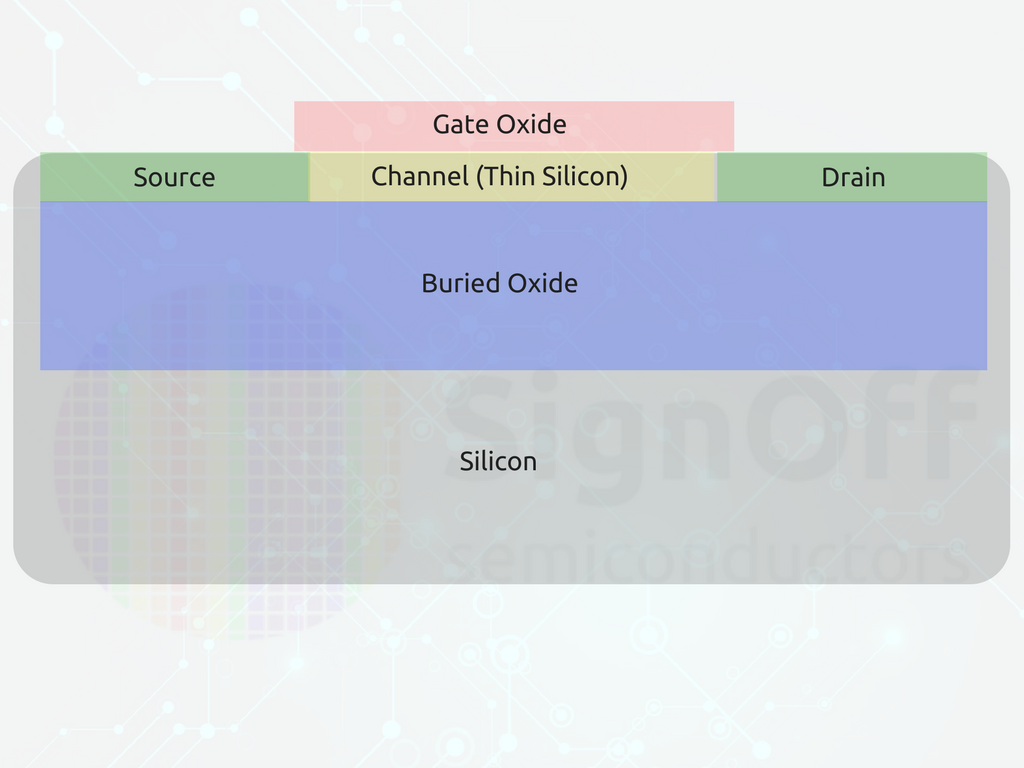
FD-SOI (UTBB-FD-SOI : Ultra thin body & buried oxide, Fully Depleted Silicon On Insulator )
Key advantages of Fully depleted SOI:
- Better electro-static control of the channel.
- No doping required
- Limited short channel effects, compared to CMOS Bulk
- Minimum junction capacitance and diode leakage
- Low leakage power
FinFET
Scaling became very difficult in planar Bulk CMOS (less than 28 nm). Below video explains the structure of FiFET deivce. This form of gate structure provides improved electrical control over the channel conduction and it helps reduce leakage current levels and overcomes some other short-channel effects.
Key advantages of FiFET:
- Low power, hence allowing high integration levels.
- FinFETs operate at a lower voltage as a result of their lower threshold voltage.
- Because of reduced short-channel effects, further device shrinking id possible.
- Very less leakage current
- Improved operating speed
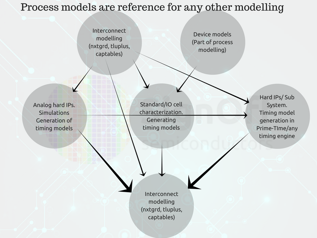
Process modelling
Process modelling is predict geometries and material properties of the wafer structures and semiconductor devices as they result from the manufacturing process. We will be discussing the use of process models (spice models) for timing of the entire IC. Spice models of the process, are the source for any further timing model of the devices/cells/Memories/IPs/Sub Systems & Interconnect models are also used during the simulations (which may generate timing models)
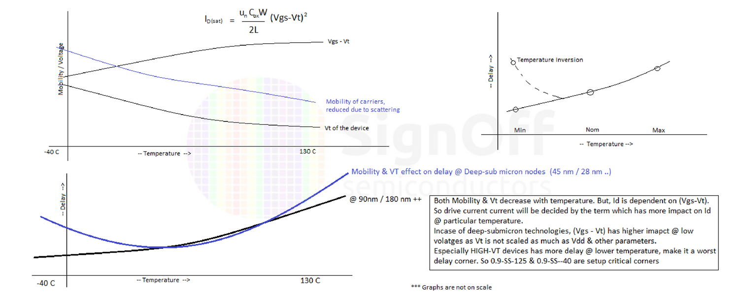
Temperature Inversion
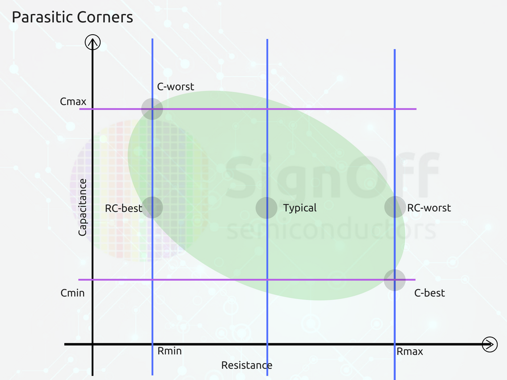
Inter Connect Variations & Parasitic Corners
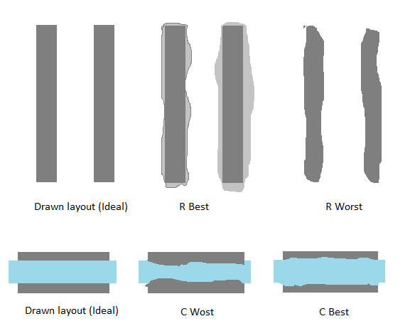
Five Parasitic corners are:
- Cbest – minimum capacitance, minimum delay (Hold analyses)
- Cworst – maximum capacitance, maximum delay (Setup analyses)
- RCbest – minimum RC product (Long interconnects)
- RCworst – maximum RC product (Long interconnects)
- Typical – nominal values of RC


 3835
3835


 被折叠的 条评论
为什么被折叠?
被折叠的 条评论
为什么被折叠?
 到【灌水乐园】发言


