Design book of spi controller with flash

  1. Overview
    1.1. Characteristics of this spi controller
    The FlashSpi module is an spi master controller that can be configured through AHB bus. It is suitable for wifi chips based on AHB bus architecture like S902, and is used to read and write off-chip
    flash chips such as S25FL116K of Spansion, W25Q20CL of Winbond or similar off-chip flash chips
    that provide spi slave interface. This module has the following features:
  1. provide a set of AHB slave interfaces, a set of DMA Single request interfaces and an interrupt request in the chip, and provide spi master interfaces outside the chip.
  2. It can provide spi clock with the fastest half of the system clock frequency.
  3. For a communication, it starts automatically after the register is configured. After the communication is completely finished, the register flag bit is displayed, and the completion interrupt can also be generated.
  4. One communication can contain up to 8 independently configurable phase, which is enough to flexibly correspond to various situations contained in one spi communication of flash chip.
  5. The whole module adopts synchronous clock design, and all signals belong to CLK clock domain.
    1.2, the concept of PHASE
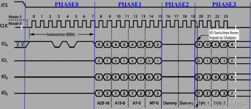
    The following figure is a typical timing diagram of reading FLASH data through SPI.
    在这里插入图片描述
    The process from CSn falling to CSn rising is called an SPI communication. In the SPI communication shown above, Instruction, A, M and Dummy should be sent in turn, and then data should be received. And Instruction only uses one line, while the subsequent processes all use four lines. Aiming at this kind of timing, this module puts forward the concept of PHASE. A communication can contain up to 8 PHASEs, and each phase can independently set parameters such as read-write
    operation, 1/2/4 line mode, communication data volume, etc. After the first SPI communication starts, this module will finish the tasks set by each PHASE in the order of PHASE0→PHASE7, and then end the SPI communication. For example, for the timing of the above figure, it can be divided into 4 PHASE.
    1.3. Module block diagram
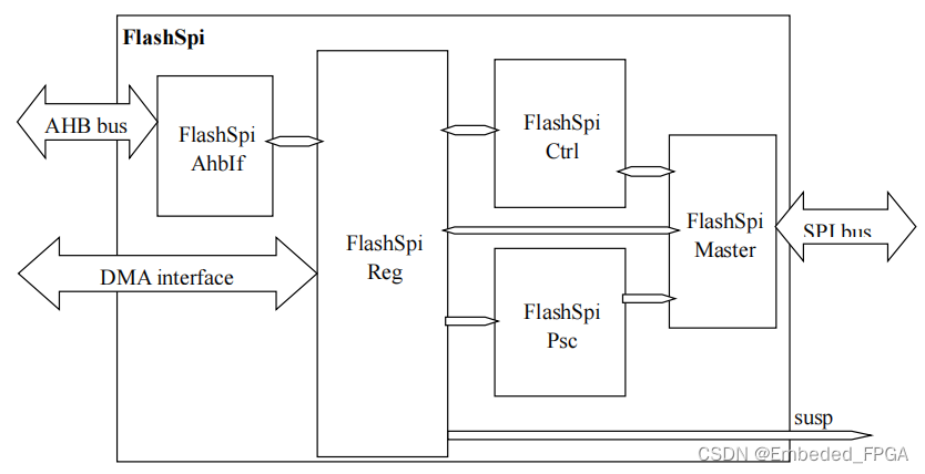
    The following figure is a block diagram of this spi controller:
    在这里插入图片描述
    FlashSpiAhbIf: an AHB Slave interface controller, which is responsible for converting the AHB bus signal into the internal read-write signal of the module and interacting with the register module FlashSpiReg to complete the read-write operation.
    Flaspireg: register module of SPI controller, in which all registers are located. At the same time, the generation and processing of DMA interface signals and the generation of interrupts are also in this module.
    Flaspictrl: the core control module of SPI controller. When it is detected that the SPI_START bit in FlashSpiReg is written as 1, the phase set in the register is analyzed to generate control and data for FlashSpiDataPump.
    FlashSpiPsc:spi sck clock controller, used to control the frequency of sck clock.
    FlashSpimaster: Spimaster interface controller, which controls the spi bus to send and receive according to the control signal sent by FlashSpiCtrl.

1.4. Top port
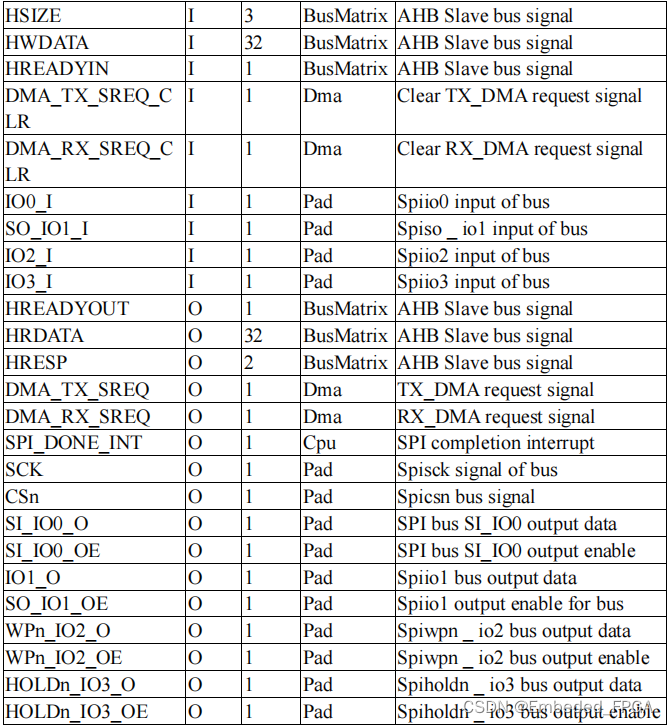
The following is a list of top-level ports and functions of this module:在这里插入图片描述
在这里插入图片描述
2. Instructions for use of the module
2.1. System integration method
The integration of AHB bus, DMA interface and interrupt interface is relatively simple, which will not be described here. The integration of SPI bus should be equivalent to the following logic:在这里插入图片描述
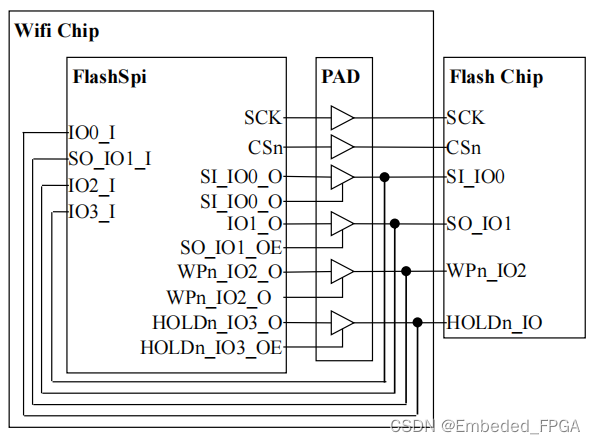
In addition, in order to prevent the input from floating, it is best to add a pull up resistor between Wifi Chip and Flash Chip.

  • 19
    点赞
  • 23
    收藏
    觉得还不错? 一键收藏
  • 0
    评论
完整版:https://download.csdn.net/download/qq_27595745/89522468 【课程大纲】 1-1 什么是java 1-2 认识java语言 1-3 java平台的体系结构 1-4 java SE环境安装和配置 2-1 java程序简介 2-2 计算机中的程序 2-3 java程序 2-4 java类库组织结构和文档 2-5 java虚拟机简介 2-6 java的垃圾回收器 2-7 java上机练习 3-1 java语言基础入门 3-2 数据的分类 3-3 标识符、关键字和常量 3-4 运算符 3-5 表达式 3-6 顺序结构和选择结构 3-7 循环语句 3-8 跳转语句 3-9 MyEclipse工具介绍 3-10 java基础知识章节练习 4-1 一维数组 4-2 数组应用 4-3 多维数组 4-4 排序算法 4-5 增强for循环 4-6 数组和排序算法章节练习 5-0 抽象和封装 5-1 面向过程的设计思想 5-2 面向对象的设计思想 5-3 抽象 5-4 封装 5-5 属性 5-6 方法的定义 5-7 this关键字 5-8 javaBean 5-9 包 package 5-10 抽象和封装章节练习 6-0 继承和多态 6-1 继承 6-2 object类 6-3 多态 6-4 访问修饰符 6-5 static修饰符 6-6 final修饰符 6-7 abstract修饰符 6-8 接口 6-9 继承和多态 章节练习 7-1 面向对象的分析与设计简介 7-2 对象模型建立 7-3 类之间的关系 7-4 软件的可维护与复用设计原则 7-5 面向对象的设计与分析 章节练习 8-1 内部类与包装器 8-2 对象包装器 8-3 装箱和拆箱 8-4 练习题 9-1 常用类介绍 9-2 StringBuffer和String Builder类 9-3 Rintime类的使用 9-4 日期类简介 9-5 java程序国际化的实现 9-6 Random类和Math类 9-7 枚举 9-8 练习题 10-1 java异常处理 10-2 认识异常 10-3 使用try和catch捕获异常 10-4 使用throw和throws引发异常 10-5 finally关键字 10-6 getMessage和printStackTrace方法 10-7 异常分类 10-8 自定义异常类 10-9 练习题 11-1 Java集合框架和泛型机制 11-2 Collection接口 11-3 Set接口实现类 11-4 List接口实现类 11-5 Map接口 11-6 Collections类 11-7 泛型概述 11-8 练习题 12-1 多线程 12-2 线程的生命周期 12-3 线程的调度和优先级 12-4 线程的同步 12-5 集合类的同步问题 12-6 用Timer类调度任务 12-7 练习题 13-1 Java IO 13-2 Java IO原理 13-3 流类的结构 13-4 文件流 13-5 缓冲流 13-6 转换流 13-7 数据流 13-8 打印流 13-9 对象流 13-10 随机存取文件流 13-11 zip文件流 13-12 练习题 14-1 图形用户界面设计 14-2 事件处理机制 14-3 AWT常用组件 14-4 swing简介 14-5 可视化开发swing组件 14-6 声音的播放和处理 14-7 2D图形的绘制 14-8 练习题 15-1 反射 15-2 使用Java反射机制 15-3 反射与动态代理 15-4 练习题 16-1 Java标注 16-2 JDK内置的基本标注类型 16-3 自定义标注类型 16-4 对标注进行标注 16-5 利用反射获取标注信息 16-6 练习题 17-1 顶目实战1-单机版五子棋游戏 17-2 总体设计 17-3 代码实现 17-4 程序的运行与发布 17-5 手动生成可执行JAR文件 17-6 练习题 18-1 Java数据库编程 18-2 JDBC类和接口 18-3 JDBC操作SQL 18-4 JDBC基本示例 18-5 JDBC应用示例 18-6 练习题 19-1 。。。
Verilog is a hardware description language used for designing digital circuits. SPI (Serial Peripheral Interface) flash is a type of non-volatile memory used in embedded systems to store program code, configuration data, and user data. To interface a Verilog design with an SPI flash, the Verilog code needs to communicate with the SPI flash using the SPI protocol. This involves sending and receiving data on the SPI bus, which consists of four signals: SCLK, MOSI, MISO, and SS. The SCLK signal is the clock signal used to synchronize the data transfer between the Verilog design and the SPI flash. The MOSI signal is the Master Out Slave In signal, used to send data from the Verilog design to the SPI flash. The MISO signal is the Master In Slave Out signal, used to send data from the SPI flash to the Verilog design. The SS signal is the Slave Select signal, used to select the SPI flash for communication. To interface with an SPI flash, the Verilog code needs to implement a SPI controller that can send and receive data on the SPI bus. The SPI controller needs to be able to send commands to the SPI flash to read, write, erase, or modify data stored in the flash memory. Once the SPI controller is implemented in Verilog, it can be integrated into a larger design, such as a microcontroller or FPGA, to create an embedded system that can communicate with an SPI flash. This enables the system to store and retrieve data from the flash memory, which can be used for various purposes, such as booting the system, storing configuration data, or logging data.

“相关推荐”对你有帮助么?

  • 非常没帮助
  • 没帮助
  • 一般
  • 有帮助
  • 非常有帮助
提交
评论
添加红包

请填写红包祝福语或标题

红包个数最小为10个

红包金额最低5元

当前余额3.43前往充值 >
需支付:10.00
成就一亿技术人!
领取后你会自动成为博主和红包主的粉丝 规则
hope_wisdom
发出的红包
实付
使用余额支付
点击重新获取
扫码支付
钱包余额 0

抵扣说明:

1.余额是钱包充值的虚拟货币,按照1:1的比例进行支付金额的抵扣。
2.余额无法直接购买下载,可以购买VIP、付费专栏及课程。

余额充值