


项目场景:
采用两片内存256M的DDR3,扩充为内存为512M的DDR3,FPGA例化一个MIG核,控制两片ddr3芯片。
FPGA型号:xc7z020clg-484-1;
DDR3型号:MT41K128M16-107;
参看链接:
问题描述
FPGA例化一个MIG核,控制两片ddr3芯片时(采用两片256M内存的DDR3扩充为512M的内存),综合错误,提示MIG核内部存在没有连接的端口,检查后发现该端口已经连接。
VIVADO报错信息:
- [Opt 31-67] Problem: A LUT2 cell in the design is missing a connection on input pin I1, which is used by the LUT equation. This pin has either been left unconnected in the design or the connection was removed due to the trimming of unused logic. The LUT cell name is: u_mig_7series_0/u_mig_7series_0_mig/u_memc_ui_top_std/u_ui_top/ui_cmd0/app_addr_r1[26]_i_1.
原因分析:
提示:具体啥原因,那位大神知道,还请告诉我一下
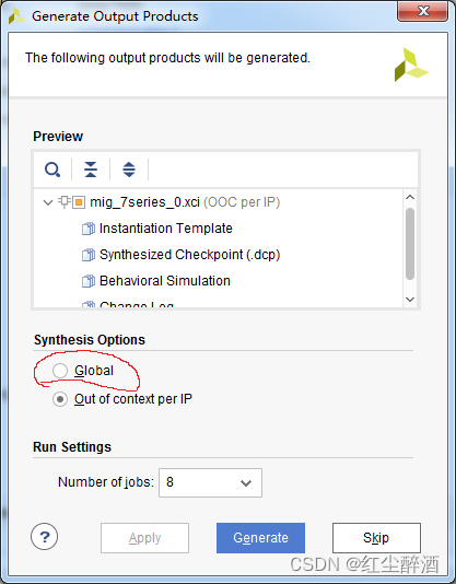
解决方案:
提示: mig例化时,最后一步,选择全局综合(Global),例化即可成功


 7201
7201


 被折叠的 条评论
为什么被折叠?
被折叠的 条评论
为什么被折叠?
 到【灌水乐园】发言


