


These objects are used to model the physical structure, define the solver region, any sources of light or doping/generation regions as well as monitors to collect data. The pages provide detailed descriptions of each simulation object. Simulation objects can be added by clicking on the corresponding icon in the GUI.
Structures
Primitives:
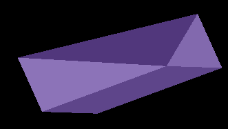
Triangle - Simulation Object
FDTD MODE DGTD CHARGE HEAT FEEM
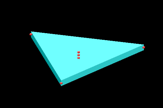
Triangular objects denote physical objects that appear triangular from above. For 2D simulations, these objects represent triangles while in 3D these objects are extruded in the z direction to a specific height. They are actually polygon objects, with the number of vertices set to 3.
Setting the vertices of the polygon object
The vertices of the polygon object can be edited by
- moving them with the mouse,
- manually editing the x,y location of each vertex in the polygon property editor,
- script command
For complex shapes, scripting in the structure group is usually best. Once the script has calculated the x,y vertex positions, they can be loaded into the polygon object with a single set("vertices",V); command. For example, use the following code to create an octagon shaped object.
# octagon properties
n_sides=8;
r=1e-6;

# x,y position of each corner
theta=linspace(0,360,n_sides+1);
theta=theta(1:n_sides);
x=r*cos(theta*pi/180);
y=r*sin(theta*pi/180);

# combine x,y into one vertices matrix
V=matrix(n_sides,2);
V(1:n_sides,1)=x(1:n_sides);
V(1:n_sides,2)=y(1:n_sides);

# add polygon object and set the vertices
addpoly;
set("vertices",V);
To get the polygon vertices, use the following command. The vertices will be returned in an Nx2 matrix. The columns of this matrix correspond to the X,Y positions of each vertex.
V=get("vertices");
?size(V);
To modify a polygon vertex, you must get the vertices matrix, modify the vertex matrix as desired, then re-apply it to the polygon object:
V=get("vertices");
V(1,1)=V(1,1)+1e-6; # change the x position of the first vertex by 1um.
set("vertices",V);
Geometry tab
- X, Y, Z: The center position of the object
- Z MIN, Z MAX: Z min, Z max position
- Z SPAN: Z span of the object
- ADD, DELETE: Add, delete vertices
Material tab
The material options are as follows:
- MATERIAL: This field can be set to any material included in the material database. It is possible to include new materials in the database, or edit the materials already included. See the material database section for more information.
- OVERRIDE MESH ORDER FROM MATERIAL DATABASE: Select to override the mesh order from the material database and manually set a mesh order. The mesh order is used by the simulation engine to select which material to use when two materials overlap. See the mesh order (optical) or mesh order (electrical) section for more details.
- MESH ORDER: Set the mesh order in this field if the OVERRIDE MESH ORDER FROM MATERIAL DATABASE option is selected. If the option is not selected, the field displays the material's default mesh order from the database. For example, a material of mesh order 1 will take precedence over a material of mesh order 2.
The following only applies to MODE and FDTD:
If <Object defined dielectric> is selected, then the INDEX property must be set.
- INDEX: The refractive index of the structure, when the material type is <Object defined dielectric>. The index must be greater than one.
- Anisotropic index: To specify an anisotropic refractive index, use a semicolon to separate the diagonal xx,yy,zz indices. Eg. 1;1.5;1
- Spatially varying index: It is possible to specify a spatially varying refractive index by entering an equation of the variables x,y,z in this field. Eg. 2+0.1*x will create an object where the refractive index increases in the X direction. The units of the spatial variables (x,y,z) must be set with the 'INDEX UNITS' property described below. The variables x,y,z will be zero in the center of the object. When using an equation in this field, consider using a mesh override region to control the simulation mesh size. For more information on entering equations, see the Equation interpreter section.
- INDEX UNITS: Only relevant when specifying a spatially varying equation in the INDEX properly described above. Specify the units (nm, um, m) of the x,y,z position variables.
- GRID ATTRIBUTE NAME: Enter the name of the grid attribute that applies to this object, see the grid attribute section
The following only applies to CHARGE, HEAT, FEEM, DGTD:
If the material chosen from the drop down menu is a binary alloy consisting of two semiconductors, then there will be an additional property, namely, the "composition fraction" to set as well.
- COMPOSITION FRACTION: This is x, the fraction of the semiconductor in the alloy. x can either take a fixed value or vary.
The user can see which semiconductor has fraction x and which has fraction (1-x) shown in a line above this drop down menu.
- FIXED: This means that fraction x will be a constant value between 0 and 1.
- LINEAR X/Y/Z: This means that the composition fraction x will vary as a function x or y or z. In this case, user can specify the min and max fraction values for the min and max spatial points and the fraction will be interpolated linearly in between. x,y,z here are those of the unrotated object. x,y,z are local to the object.
- EQUATION: The user can enter an equation for the fraction that varies with u,v and w. u is (x-x0), v is (y-y0) and w is (z-z0) where x0, y0 and z0 are the center coordinates of the object. This means that u,v and w are local to the object.
Rotation tab
Rotate objects by setting the following variables:
- FIRST, SECOND, THIRD AXES: Select rotation axis. Up to three different rotations can be applied.
- ROTATION 1,2,3: The rotation of the object in a clockwise direction about each axis, measured in degrees.
Graphical Rendering tab
The graphical rendering tab is used to change how objects are drawn in the layout editor. The options are:
- RENDER TYPE: The options for drawing the objects are detailed or wireframe. Detailed objects are shaded and their transparency can be set using OVERRIDE COLOR OPACITY FROM MATERIAL DATABASE.
- DETAIL: This is a slider which takes values between 0 and 1. By default it is set to 0.5. Higher detail shows more detail, but increases the time required to draw objects. This setting has no effect on the simulation.
- OVERRIDE COLOR OPACITY FROM MATERIAL DATABASE: When unselected the opacity is determined from the material database. When selected, you can specify a value for ALPHA between 0 (transparent) and 1 (opaque) for the object, depending on how transparent you want the object to be.
Rectangle - Simulation Object
FDTD MODE DGTD CHARGE HEAT FEEM
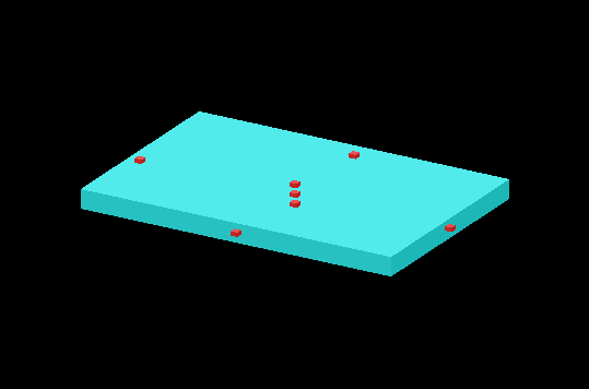
Rectangular regions denote physical objects that appear rectangular from above. For 2D simulations, these objects represent rectangles while in 3D these objects are extruded to a specific height.
Geometry tab
- X, Y, Z: The center position of the object
- X MIN, X MAX: X min, X max position
- Y MIN, Y MAX: Y min, Y max position
- Z MIN, Z MAX: Z min, Z max position
- X SPAN, Y SPAN, Z SPAN: X, Y, Z span of the object
Material tab
The material options are as follows:
- MATERIAL: This field can be set to any material included in the material database. It is possible to include new materials in the database, or edit the materials already included. See the material database section for more information.
- OVERRIDE MESH ORDER FROM MATERIAL DATABASE: Select to override the mesh order from the material database and manually set a mesh order. The mesh order is used by the simulation engine to select which material to use when two materials overlap. See the mesh order (optical) or mesh order (electrical) section for more details.
- MESH ORDER: Set the mesh order in this field if the OVERRIDE MESH ORDER FROM MATERIAL DATABASE option is selected. If the option is not selected, the field displays the material's default mesh order from the database. For example, a material of mesh order 1 will take precedence over a material of mesh order 2.
The following only applies to MODE and FDTD:
If <Object defined dielectric> is selected, then the INDEX property must be set.
- INDEX: The refractive index of the structure, when the material type is <Object defined dielectric>. The index must be greater than one.
-
-
- Anisotropic index: To specify an anisotropic refractive index, use a semicolon to separate the diagonal xx,yy,zz indices. Eg. 1;1.5;1
- Spatially varying index: It is possible to specify a spatially varying refractive index by entering an equation of the variables x,y,z in this field. Eg. 2+0.1*x will create an object where the refractive index increases in the X direction. The units of the spatial variables (x,y,z) must be set with the 'INDEX UNITS' property described below. The variables x,y,z will be zero in the center of the object. When using an equation in this field, consider using a mesh override region to control the simulation mesh size. For more information on entering equations, see the Equation interpreter section.
-
- INDEX UNITS: Only relevant when specifying a spatially varying equation in the INDEX properly described above. Specify the units (nm, um, m) of the x,y,z position variables.
- GRID ATTRIBUTE NAME: Enter the name of the grid attribute that applies to this object, see the grid attribute section
The following only applies to CHARGE, HEAT, FEEM, DGTD:
If the material chosen from the drop down menu is a binary alloy consisting of two semiconductors, then there will be an additional property, namely, the "composition fraction" to set as well.
- COMPOSITION FRACTION: This is x, the fraction of the semiconductor in the alloy. x can either take a fixed value or vary.
The user can see which semiconductor has fraction x and which has fraction (1-x) shown in a line above this drop down menu.
- FIXED: This means that fraction x will be a constant value between 0 and 1.
- LINEAR X/Y/Z: This means that the composition fraction x will vary as a function x or y or z. In this case, user can specify the min and max fraction values for the min and max spatial points and the fraction will be interpolated linearly in between. x,y,z here are those of the unrotated object. x,y,z are local to the object.
- EQUATION: The user can enter an equation for the fraction that varies with u,v and w. u is (x-x0), v is (y-y0) and w is (z-z0) where x0, y0 and z0 are the center coordinates of the object. This means that u,v and w are local to the object.
Rotation tab
Rotate objects by setting the following variables:
- FIRST, SECOND, THIRD AXES: Select rotation axis. Up to three different rotations can be applied.
- ROTATION 1,2,3: The rotation of the object in a clockwise direction about each axis, measured in degrees.
Graphical Rendering tab
The graphical rendering tab is used to change how objects are drawn in the layout editor. The options are:
- RENDER TYPE: The options for drawing the objects are detailed or wireframe. Detailed objects are shaded and their transparency can be set using OVERRIDE COLOR OPACITY FROM MATERIAL DATABASE.
- DETAIL: This is a slider which takes values between 0 and 1. By default it is set to 0.5. Higher detail shows more detail, but increases the time required to draw objects. This setting has no effect on the simulation.
- OVERRIDE COLOR OPACITY FROM MATERIAL DATABASE: When unselected the opacity is determined from the material database. When selected, you can specify a value for ALPHA between 0 (transparent) and 1 (opaque) for the object, depending on how transparent you want the object to be.
Polygon - Simulation Object
FDTD MODE DGTD CHARGE HEAT FEEM
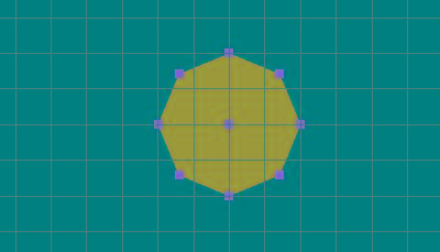
This section describes how to set and get the vertex positions of a polygon object. Polygons allow the user to define a custom object with a variable number of vertices. The location of each vertex can be independently positioned within a plane, and the vertices are connected with straight lines. For 3D simulations, the object is extruded in the z dimension. In DEVICE, the vertices have to be entered in a counter clock wise manner for the structure to be defined and meshed properly.
Setting the vertices of the polygon object
The vertices of the polygon object can be edited by
- moving them with the mouse,
- manually editing the x,y location of each vertex in the polygon property editor,
- script command
For complex shapes, scripting in the structure group is usually best. Once the script has calculated the x,y vertex positions, they can be loaded into the polygon object with a single set("vertices",V); command. For example, use the following code to create an octagon shaped object.
# octagon properties
n_sides=8;
r=1e-6;

# x,y position of each corner
theta=linspace(0,360,n_sides+1);
theta=theta(1:n_sides);
x=r*cos(theta*pi/180);
y=r*sin(theta*pi/180);

# combine x,y into one vertices matrix
V=matrix(n_sides,2);
V(1:n_sides,1)=x(1:n_sides);
V(1:n_sides,2)=y(1:n_sides);

# add polygon object and set the vertices
addpoly;
set("vertices",V);
NOTE: Getting and modifying polygon vertices
To get the polygon vertices, use the following command. The vertices will be returned in an Nx2 matrix. The columns of this matrix correspond to the X,Y positions of each vertex.
V=get("vertices");
?size(V);
To modify a polygon vertex, you must get the vertices matrix, modify the vertex matrix as desired, then re-apply it to the polygon object:
V=get("vertices");
V(1,1)=V(1,1)+1e-6; # change the x position of the first vertex by 1um.
set("vertices",V);
Geometry tab
- X, Y, Z: The center position of the object
- Z MIN, Z MAX: Z min, Z max position
- Z SPAN: Z span of the object
- ADD, DELETE: Add, delete vertices
Material tab
The material options are as follows:
- MATERIAL: This field can be set to any material included in the material database. It is possible to include new materials in the database, or edit the materials already included. See the material database section for more information.
- OVERRIDE MESH ORDER FROM MATERIAL DATABASE: Select to override the mesh order from the material database and manually set a mesh order. The mesh order is used by the simulation engine to select which material to use when two materials overlap. See the mesh order (optical) or mesh order (electrical) section for more details.
- MESH ORDER: Set the mesh order in this field if the OVERRIDE MESH ORDER FROM MATERIAL DATABASE option is selected. If the option is not selected, the field displays the material's default mesh order from the database. For example, a material of mesh order 1 will take precedence over a material of mesh order 2.
The following only applies to MODE and FDTD:
- If <Object defined dielectric> is selected, then the INDEX property must be set.
- INDEX: The refractive index of the structure, when the material type is <Object defined dielectric>. The index must be greater than one.
- Anisotropic index: To specify an anisotropic refractive index, use a semicolon to separate the diagonal xx,yy,zz indices. Eg. 1;1.5;1
- Spatially varying index: It is possible to specify a spatially varying refractive index by entering an equation of the variables x,y,z in this field. Eg. 2+0.1*x will create an object where the refractive index increases in the X direction. The units of the spatial variables (x,y,z) must be set with the 'INDEX UNITS' property described below. The variables x,y,z will be zero in the center of the object. When using an equation in this field, consider using a mesh override region to control the simulation mesh size. For more information on entering equations, see the Equation interpreter section.
- INDEX UNITS: Only relevant when specifying a spatially varying equation in the INDEX properly described above. Specify the units (nm, um, m) of the x,y,z position variables.
- GRID ATTRIBUTE NAME: Enter the name of the grid attribute that applies to this object, see the grid attribute section
The following only applies to CHARGE, HEAT, FEEM, DGTD:
If the material chosen from the drop down menu is a binary alloy consisting of two semiconductors, then there will be an additional property, namely, the "composition fraction" to set as well.
- COMPOSITION FRACTION: This is x, the fraction of the semiconductor in the alloy. x can either take a fixed value or vary.
The user can see which semiconductor has fraction x and which has fraction (1-x) shown in a line above this drop down menu.
- FIXED: This means that fraction x will be a constant value between 0 and 1.
- LINEAR X/Y/Z: This means that the composition fraction x will vary as a function x or y or z. In this case, user can specify the min and max fraction values for the min and max spatial points and the fraction will be interpolated linearly in between. x,y,z here are those of the unrotated object. x,y,z are local to the object.
- EQUATION: The user can enter an equation for the fraction that varies with u,v and w. u is (x-x0), v is (y-y0) and w is (z-z0) where x0, y0 and z0 are the center coordinates of the object. This means that u,v and w are local to the object.
Rotation tab
Rotate objects by setting the following variables:
- FIRST, SECOND, THIRD AXES: Select rotation axis. Up to three different rotations can be applied.
- ROTATION 1,2,3: The rotation of the object in a clockwise direction about each axis, measured in degrees.
Graphical Rendering tab
The graphical rendering tab is used to change how objects are drawn in the layout editor. The options are:
- RENDER TYPE: The options for drawing the objects are detailed or wireframe. Detailed objects are shaded and their transparency can be set using OVERRIDE COLOR OPACITY FROM MATERIAL DATABASE.
- DETAIL: This is a slider which takes values between 0 and 1. By default it is set to 0.5. Higher detail shows more detail, but increases the time required to draw objects. This setting has no effect on the simulation.
- OVERRIDE COLOR OPACITY FROM MATERIAL DATABASE: When unselected the opacity is determined from the material database. When selected, you can specify a value for ALPHA between 0 (transparent) and 1 (opaque) for the object, depending on how transparent you want the object to be.
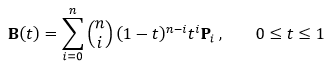
Circle - Simulation Object
FDTD MODE DGTD CHARGE HEAT FEEM
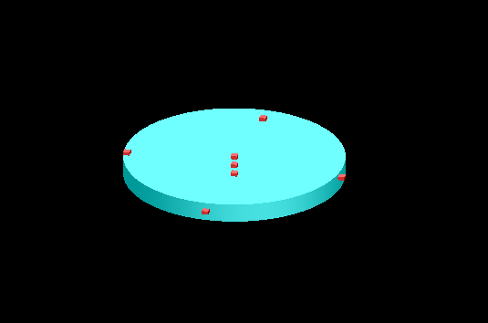
Circles denote physical objects which appear circular or ellipsoid from above. They are either circles/ellipses in 2D, or circular/ellipsoid cylinders in 3D.
Geometry tab
- X, Y, Z: The center position of the object
- Z MIN, Z MAX: Z min, Z max position
- Z SPAN: Z span of the object
- RADIUS: Radius of the object
- MAKE ELLIPSOID: If this box is checked, a second radius can be defined
Material tab
The material options are as follows:
- MATERIAL: This field can be set to any material included in the material database. It is possible to include new materials in the database, or edit the materials already included. See the material database section for more information.
- OVERRIDE MESH ORDER FROM MATERIAL DATABASE: Select to override the mesh order from the material database and manually set a mesh order. The mesh order is used by the simulation engine to select which material to use when two materials overlap. See the mesh order (optical) or mesh order (electrical) section for more details.
- MESH ORDER: Set the mesh order in this field if the OVERRIDE MESH ORDER FROM MATERIAL DATABASE option is selected. If the option is not selected, the field displays the material's default mesh order from the database. For example, a material of mesh order 1 will take precedence over a material of mesh order 2.
The following only applies to MODE and FDTD:
If <Object defined dielectric> is selected, then the INDEX property must be set.
- INDEX: The refractive index of the structure, when the material type is <Object defined dielectric>. The index must be greater than one.
-
-
- Anisotropic index: To specify an anisotropic refractive index, use a semicolon to separate the diagonal xx,yy,zz indices. Eg. 1;1.5;1
- Spatially varying index: It is possible to specify a spatially varying refractive index by entering an equation of the variables x,y,z in this field. Eg. 2+0.1*x will create an object where the refractive index increases in the X direction. The units of the spatial variables (x,y,z) must be set with the 'INDEX UNITS' property described below. The variables x,y,z will be zero in the center of the object. When using an equation in this field, consider using a mesh override region to control the simulation mesh size. For more information on entering equations, see the Equation interpreter section.
-
- INDEX UNITS: Only relevant when specifying a spatially varying equation in the INDEX properly described above. Specify the units (nm, um, m) of the x,y,z position variables.
- GRID ATTRIBUTE NAME: Enter the name of the grid attribute that applies to this object, see the grid attribute section
The following only applies to CHARGE, HEAT, FEEM, DGTD:
If the material chosen from the drop down menu is a binary alloy consisting of two semiconductors, then there will be an additional property, namely, the "composition fraction" to set as well.
- COMPOSITION FRACTION: This is x, the fraction of the semiconductor in the alloy. x can either take a fixed value or vary.
The user can see which semiconductor has fraction x and which has fraction (1-x) shown in a line above this drop down menu.
- FIXED: This means that fraction x will be a constant value between 0 and 1.
- LINEAR X/Y/Z: This means that the composition fraction x will vary as a function x or y or z. In this case, user can specify the min and max fraction values for the min and max spatial points and the fraction will be interpolated linearly in between. x,y,z here are those of the unrotated object. x,y,z are local to the object.
- EQUATION: The user can enter an equation for the fraction that varies with u,v and w. u is (x-x0), v is (y-y0) and w is (z-z0) where x0, y0 and z0 are the center coordinates of the object. This means that u,v and w are local to the object.
Rotation tab
Rotate objects by setting the following variables:
- FIRST, SECOND, THIRD AXES: Select rotation axis. Up to three different rotations can be applied.
- ROTATION 1,2,3: The rotation of the object in a clockwise direction about each axis, measured in degrees.
Graphical Rendering tab
The graphical rendering tab is used to change how objects are drawn in the layout editor. The options are:
- RENDER TYPE: The options for drawing the objects are detailed or wireframe. Detailed objects are shaded and their transparency can be set using OVERRIDE COLOR OPACITY FROM MATERIAL DATABASE.
- DETAIL: This is a slider which takes values between 0 and 1. By default it is set to 0.5. Higher detail shows more detail, but increases the time required to draw objects. This setting has no effect on the simulation.
- OVERRIDE COLOR OPACITY FROM MATERIAL DATABASE: When unselected the opacity is determined from the material database. When selected, you can specify a value for ALPHA between 0 (transparent) and 1 (opaque) for the object, depending on how transparent you want the object to be.
Ring - Simulation Object
FDTD MODE DGTD CHARGE HEAT FEEM
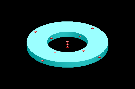
Ring regions represent physical objects that consist of full or partial rings when viewed from above. Rings in 3D simulations are extruded in the z direction to a specific height.
Geometry tab
- X, Y, Z: The center position of the object
- Z MIN, Z MAX: Z min, Z max position
- Z SPAN: Z span of the object
- OUTER RADIUS, INNER RADIUS: Outer and inner radius of the ring
- THETA START, THETA STOP: Specify the angle range that ring to be drawn, in degree.
- MAKE ELLIPSOID: if this box is checked, a second outer and inner radius can be defined
Material tab
The material options are as follows:
- MATERIAL: This field can be set to any material included in the material database. It is possible to include new materials in the database, or edit the materials already included. See the material database section for more information.
- OVERRIDE MESH ORDER FROM MATERIAL DATABASE: Select to override the mesh order from the material database and manually set a mesh order. The mesh order is used by the simulation engine to select which material to use when two materials overlap. See the mesh order (optical) or mesh order (electrical) section for more details.
- MESH ORDER: Set the mesh order in this field if the OVERRIDE MESH ORDER FROM MATERIAL DATABASE option is selected. If the option is not selected, the field displays the material's default mesh order from the database. For example, a material of mesh order 1 will take precedence over a material of mesh order 2.
The following only applies to MODE and FDTD:
If <Object defined dielectric> is selected, then the INDEX property must be set.
- INDEX: The refractive index of the structure, when the material type is <Object defined dielectric>. The index must be greater than one.
-
-
- Anisotropic index: To specify an anisotropic refractive index, use a semicolon to separate the diagonal xx,yy,zz indices. Eg. 1;1.5;1
- Spatially varying index: It is possible to specify a spatially varying refractive index by entering an equation of the variables x,y,z in this field. Eg. 2+0.1*x will create an object where the refractive index increases in the X direction. The units of the spatial variables (x,y,z) must be set with the 'INDEX UNITS' property described below. The variables x,y,z will be zero in the center of the object. When using an equation in this field, consider using a mesh override region to control the simulation mesh size. For more information on entering equations, see the Equation interpreter section.
-
- INDEX UNITS: Only relevant when specifying a spatially varying equation in the INDEX properly described above. Specify the units (nm, um, m) of the x,y,z position variables.
- GRID ATTRIBUTE NAME: Enter the name of the grid attribute that applies to this object, see the grid attribute section
The following only applies to CHARGE, HEAT, FEEM, DGTD:
If the material chosen from the drop down menu is a binary alloy consisting of two semiconductors, then there will be an additional property, namely, the "composition fraction" to set as well.
- COMPOSITION FRACTION: This is x, the fraction of the semiconductor in the alloy. x can either take a fixed value or vary.
The user can see which semiconductor has fraction x and which has fraction (1-x) shown in a line above this drop down menu.
- FIXED: This means that fraction x will be a constant value between 0 and 1.
- LINEAR X/Y/Z: This means that the composition fraction x will vary as a function x or y or z. In this case, user can specify the min and max fraction values for the min and max spatial points and the fraction will be interpolated linearly in between. x,y,z here are those of the unrotated object. x,y,z are local to the object.
- EQUATION: The user can enter an equation for the fraction that varies with u,v and w. u is (x-x0), v is (y-y0) and w is (z-z0) where x0, y0 and z0 are the center coordinates of the object. This means that u,v and w are local to the object.
Rotation tab
Rotate objects by setting the following variables:
- FIRST, SECOND, THIRD AXES: Select rotation axis. Up to three different rotations can be applied.
- ROTATION 1,2,3: The rotation of the object in a clockwise direction about each axis, measured in degrees.
Graphical Rendering tab
The graphical rendering tab is used to change how objects are drawn in the layout editor. The options are:
- RENDER TYPE: The options for drawing the objects are detailed or wireframe. Detailed objects are shaded and their transparency can be set using OVERRIDE COLOR OPACITY FROM MATERIAL DATABASE.
- DETAIL: This is a slider which takes values between 0 and 1. By default it is set to 0.5. Higher detail shows more detail, but increases the time required to draw objects. This setting has no effect on the simulation.
- OVERRIDE COLOR OPACITY FROM MATERIAL DATABASE: When unselected the opacity is determined from the material database. When selected, you can specify a value for ALPHA between 0 (transparent) and 1 (opaque) for the object, depending on how transparent you want the object to be.
Custom structure object - Simulation Object
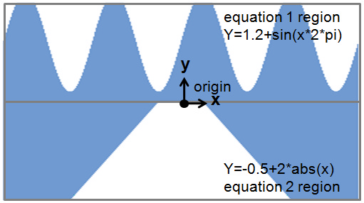
Custom primitives are objects that are defined by equations describing the boundaries of the physical object. The custom primitive defaults to a rectangular region upon creation, and is shaped via the entry of one or more equations in the edit window. The custom object allows you to define the y position of the object as a function of the x position. The z position is obtained via extrusion or revolution of the y edge. (X,Y)=(0,0) corresponds to the center of the object.
Geometry tab
- X, Y, Z: The center position of the object
- X MIN, X MAX: X min, X max position
- Y MIN, Y MAX: Y min, Y max position
- Z MIN, Z MAX: Z min, Z max position
- X SPAN, Y SPAN, Z SPAN: X, Y, Z span of the object
Custom tab
- EQUATION 1: Defines the equation in the upper region (y>0
- )
- MAKE NONSYMMETRIC: Enabled only when creating the object by extrusion
-
- EQUATION 2: Defines the equation in the lower region (y<0
-
-
-
- )
-
- EQUATION UNITS: The units used in the equation. (Default: microns)
- CREATE 3D OBJECT BY: Choose whether to define the 3D object by revolution or extrusion.
Material tab
The material options are as follows:
- MATERIAL: This field can be set to any material included in the material database. It is possible to include new materials in the database, or edit the materials already included. See the material database section for more information.
- OVERRIDE MESH ORDER FROM MATERIAL DATABASE: Select to override the mesh order from the material database and manually set a mesh order. The mesh order is used by the simulation engine to select which material to use when two materials overlap. See the mesh order (optical) or mesh order (electrical) section for more details.
- MESH ORDER: Set the mesh order in this field if the OVERRIDE MESH ORDER FROM MATERIAL DATABASE option is selected. If the option is not selected, the field displays the material's default mesh order from the database. For example, a material of mesh order 1 will take precedence over a material of mesh order 2.
The following only applies to MODE and FDTD:
If <Object defined dielectric> is selected, then the INDEX property must be set.
- INDEX: The refractive index of the structure, when the material type is <Object defined dielectric>. The index must be greater than one.
- Anisotropic index: To specify an anisotropic refractive index, use a semicolon to separate the diagonal xx,yy,zz indices. Eg. 1;1.5;1
- Spatially varying index: It is possible to specify a spatially varying refractive index by entering an equation of the variables x,y,z in this field. Eg. 2+0.1*x will create an object where the refractive index increases in the X direction. The units of the spatial variables (x,y,z) must be set with the 'INDEX UNITS' property described below. The variables x,y,z will be zero in the center of the object. When using an equation in this field, consider using a mesh override region to control the simulation mesh size. For more information on entering equations, see the Equation interpreter section.
- INDEX UNITS: Only relevant when specifying a spatially varying equation in the INDEX properly described above. Specify the units (nm, um, m) of the x,y,z position variables.
- GRID ATTRIBUTE NAME: Enter the name of the grid attribute that applies to this object, see the grid attribute section
The following only applies to CHARGE, HEAT, FEEM, DGTD:
If the material chosen from the drop down menu is a binary alloy consisting of two semiconductors, then there will be an additional property, namely, the "composition fraction" to set as well.
- COMPOSITION FRACTION: This is x, the fraction of the semiconductor in the alloy. x can either take a fixed value or vary.
The user can see which semiconductor has fraction x and which has fraction (1-x) shown in a line above this drop down menu.
- FIXED: This means that fraction x will be a constant value between 0 and 1.
- LINEAR X/Y/Z: This means that the composition fraction x will vary as a function x or y or z. In this case, user can specify the min and max fraction values for the min and max spatial points and the fraction will be interpolated linearly in between. x,y,z here are those of the unrotated object. x,y,z are local to the object.
- EQUATION: The user can enter an equation for the fraction that varies with u,v and w. u is (x-x0), v is (y-y0) and w is (z-z0) where x0, y0 and z0 are the center coordinates of the object. This means that u,v and w are local to the object.
Rotation tab
Rotate objects by setting the following variables:
- FIRST, SECOND, THIRD AXES: Select rotation axis. Up to three different rotations can be applied.
- ROTATION 1,2,3: The rotation of the object in a clockwise direction about each axis, measured in degrees.
Graphical Rendering tab
The graphical rendering tab is used to change how objects are drawn in the layout editor. The options are:
- RENDER TYPE: The options for drawing the objects are detailed or wireframe. Detailed objects are shaded and their transparency can be set using OVERRIDE COLOR OPACITY FROM MATERIAL DATABASE.
- DETAIL: This is a slider which takes values between 0 and 1. By default it is set to 0.5. Higher detail shows more detail, but increases the time required to draw objects. This setting has no effect on the simulation.
- OVERRIDE COLOR OPACITY FROM MATERIAL DATABASE: When unselected the opacity is determined from the material database. When selected, you can specify a value for ALPHA between 0 (transparent) and 1 (opaque) for the object, depending on how transparent you want the object to be.
Surface structure object - Simulation Object
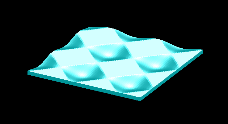
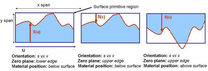
This page provides a simulation file containing several example structures created with the surface object, to demonstrate the types of structures that can be created with this object. Surface primitives can be used to define complex material volumes that exist above or below analytically defined surfaces. In 3D simulations, a surface (S) is defined as a function of variables u and v, i.e. S = S(u,v). The variables (u,v) can represent (x,y), (x,z) or (y,z) depending on the surface orientation. Similarly, in 2D simulations, a surface is defined as a function of u (S = S(u)) where u can represent x or y.
The simulation file usr_surface_example.fsp contains several examples of surface objects that can be created using conic, polynomial, and custom equation options. More examples of the surface objects can be found in the object library available in FDTD.
| Note: Drawing resolution Initially the object will be drawn at a low resolution, as shown in the top half of this figure. You can increase the drawing resolution with the settings on the Graphical rendering tab. The bottom half of this figure shows the object displayed at the same resolution as the image that is was imported from. It is important to note that the graphical rendering does not affect the simulation. Irrespective of the drawing resolution, the meshed object used for the simulation is always as has been defined. |
The custom tab is only available for surface primitives in MODE and FDTD. The diagrams below show how the surface is used to create a volume of desired material.
The surface equation can contain up to three terms, conic, polynomial and custom which are added together to create the total surface. Not all terms have to be included.
S=Sconic+Spolynomial+Scustom
Conic term:
Sconic=cr21+√1−(κ+1)c2r2
c = 1/R, c is the inverse of the radius of curvature of the surface at r = 0.
- κ
is the conic constant. When κ=−1 we have a parabolic surface. When κ=0
- we have a spherical surface.
- r2 = u2 + v2.
Polynomial term:
Spolynomial=∑5i,j=0Mijuivj
- There are 36 available coefficients
Custom term:
Scustom=f(u,v)
- You can choose any analytic function of (u,v).
- The syntax and functions available to specify the index are found in the Equation interpreter section.
For example, you could use
Scustom=sin(u+v)
Geometry tab
- X, Y, Z: The center position of the object
- X MIN, X MAX: X min, X max position
- Y MIN, Y MAX: Y min, Y max position
- Z MIN, Z MAX: Z min, Z max position
- X SPAN, Y SPAN, Z SPAN: X, Y, Z span of the object
Surface tab
- ORIENTATION: The surface determines if S is a function of (x,y), (x,z) or (y,z)..
- ZERO PLANE: This determines if surface is measured from the lower edge of the rectangular volume or the upper edge. See diagrams above.
- MATERIAL POSITION: This determines if the material fills the regions above the surface or below the surface. See diagrams above.
- SET UNDEFINED TERMS TO: It is possible that the surface equation becomes undefined. For example, it could be sqrt(-1) for some values of (u,v). In this case, the surface function will become either zero or the maximum value allowed by the rectangular volume encompassing the surface object.
- U0, V0: The origin of the (u,v) coordinate system, If U0, V0 are zero, then (u,v) = (0,0) will correspond to the center of the surface object. Setting these values to non-zero will offset the origin by a desired amount.
- SURFACE UNITS: All quantities defining the surface must be measured in the same units. You can choose these units with this menu.
- CONIC: Check this option to include the conic term in the surface equation. If this is checked, then set
- RADIUS OF CURVATURE: curvature of the surface at the origin. This is equal to the inverse of the parameter c described in the definition of Sconic.
- CONIC CONSTANT: The k constant.
- CUSTOM: Check this option to include the custom term in the surface equation
- EQUATION: The equation as a function u and v.
- POLYNOMIAL: Check this option to include a polynomial term in the surface equation. If this option is checked, the M coefficients as explained above can be entered into a table.
To import a surface object, please see Import object surfaces
Material tab
The material options are as follows:
- MATERIAL: This field can be set to any material included in the material database. It is possible to include new materials in the database, or edit the materials already included. See the material database section for more information.
- OVERRIDE MESH ORDER FROM MATERIAL DATABASE: Select to override the mesh order from the material database and manually set a mesh order. The mesh order is used by the simulation engine to select which material to use when two materials overlap. See the mesh order (optical) or mesh order (electrical) section for more details.
- MESH ORDER: Set the mesh order in this field if the OVERRIDE MESH ORDER FROM MATERIAL DATABASE option is selected. If the option is not selected, the field displays the material's default mesh order from the database. For example, a material of mesh order 1 will take precedence over a material of mesh order 2.
The following only applies to MODE and FDTD:
If <Object defined dielectric> is selected, then the INDEX property must be set.
- INDEX: The refractive index of the structure, when the material type is <Object defined dielectric>. The index must be greater than one.
- Anisotropic index: To specify an anisotropic refractive index, use a semicolon to separate the diagonal xx,yy,zz indices. Eg. 1;1.5;1
- Spatially varying index: It is possible to specify a spatially varying refractive index by entering an equation of the variables x,y,z in this field. Eg. 2+0.1*x will create an object where the refractive index increases in the X direction. The units of the spatial variables (x,y,z) must be set with the 'INDEX UNITS' property described below. The variables x,y,z will be zero in the center of the object. When using an equation in this field, consider using a mesh override region to control the simulation mesh size. For more information on entering equations, see the Equation interpreter section.
- INDEX UNITS: Only relevant when specifying a spatially varying equation in the INDEX properly described above. Specify the units (nm, um, m) of the x,y,z position variables.
- GRID ATTRIBUTE NAME: Enter the name of the grid attribute that applies to this object, see the grid attribute section
The following only applies to CHARGE, HEAT, FEEM, DGTD:
If the material chosen from the drop down menu is a binary alloy consisting of two semiconductors, then there will be an additional property, namely, the "composition fraction" to set as well.
- COMPOSITION FRACTION: This is x, the fraction of the semiconductor in the alloy. x can either take a fixed value or vary.
The user can see which semiconductor has fraction x and which has fraction (1-x) shown in a line above this drop down menu.
- FIXED: This means that fraction x will be a constant value between 0 and 1.
- LINEAR X/Y/Z: This means that the composition fraction x will vary as a function x or y or z. In this case, user can specify the min and max fraction values for the min and max spatial points and the fraction will be interpolated linearly in between. x,y,z here are those of the unrotated object. x,y,z are local to the object.
- EQUATION: The user can enter an equation for the fraction that varies with u,v and w. u is (x-x0), v is (y-y0) and w is (z-z0) where x0, y0 and z0 are the center coordinates of the object. This means that u,v and w are local to the object.
Rotation tab
Rotate objects by setting the following variables:
- FIRST, SECOND, THIRD AXES: Select rotation axis. Up to three different rotations can be applied.
- ROTATION 1,2,3: The rotation of the object in a clockwise direction about each axis, measured in degrees.
Graphical Rendering tab
The graphical rendering tab is used to change how objects are drawn in the layout editor. The options are:
- RENDER TYPE: The options for drawing the objects are detailed or wireframe. Detailed objects are shaded and their transparency can be set using OVERRIDE COLOR OPACITY FROM MATERIAL DATABASE.
- DETAIL: This is a slider which takes values between 0 and 1. By default it is set to 0.5. Higher detail shows more detail, but increases the time required to draw objects. This setting has no effect on the simulation.
- OVERRIDE COLOR OPACITY FROM MATERIAL DATABASE: When unselected the opacity is determined from the material database. When selected, you can specify a value for ALPHA between 0 (transparent) and 1 (opaque) for the object, depending on how transparent you want the object to be.
Waveguide - Simulation Object
FDTD MODE DGTD CHARGE HEAT FEEM
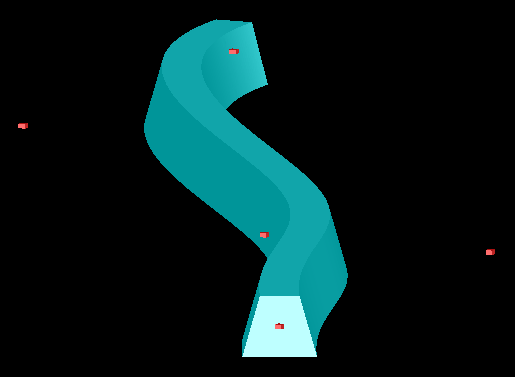
This section describes how to create a waveguide having an isosceles trapezoidal cross section and a Bézier-curved path.
Bézier curves are widely used in computer graphics for the generation of smooth curves. The path of the curve, B(t), are defined by a set of control points, called poles, P0, P1, ...., Pn and its mathematical representation is as follows:
where
![]()
is the binomial coefficients.
For n=1, the curve reduces to a straight line defined by the interpolation of the points P0 and P1.

For n=3, the curves are called cubic Bézier curves, which, together with quadratic (n=2) ones, are most commonly used . Some of the cubic Bezier curve examples are shown below.

Geometry tab
- X, Y, Z: The center position of the object
- Base width, Base height, Base Angle: The width, height, sidewall angle of the waveguide cross section
- Poles: Positions of Bezier poles.
Material tab
The material options are as follows:
- MATERIAL: This field can be set to any material included in the material database. It is possible to include new materials in the database, or edit the materials already included. See the material database section for more information.
- OVERRIDE MESH ORDER FROM MATERIAL DATABASE: Select to override the mesh order from the material database and manually set a mesh order. The mesh order is used by the simulation engine to select which material to use when two materials overlap. See the mesh order (optical) or mesh order (electrical) section for more details.
- MESH ORDER: Set the mesh order in this field if the OVERRIDE MESH ORDER FROM MATERIAL DATABASE option is selected. If the option is not selected, the field displays the material's default mesh order from the database. For example, a material of mesh order 1 will take precedence over a material of mesh order 2.
The following only applies to MODE and FDTD:
If <Object defined dielectric> is selected, then the INDEX property must be set.
- INDEX: The refractive index of the structure, when the material type is <Object defined dielectric>. The index must be greater than one.
-
-
- Anisotropic index: To specify an anisotropic refractive index, use a semicolon to separate the diagonal xx,yy,zz indices. Eg. 1;1.5;1
- Spatially varying index: It is possible to specify a spatially varying refractive index by entering an equation of the variables x,y,z in this field. Eg. 2+0.1*x will create an object where the refractive index increases in the X direction. The units of the spatial variables (x,y,z) must be set with the 'INDEX UNITS' property described below. The variables x,y,z will be zero in the center of the object. When using an equation in this field, consider using a mesh override region to control the simulation mesh size. For more information on entering equations, see the Equation interpreter section.
-
- INDEX UNITS: Only relevant when specifying a spatially varying equation in the INDEX properly described above. Specify the units (nm, um, m) of the x,y,z position variables.
- GRID ATTRIBUTE NAME: Enter the name of the grid attribute that applies to this object, see the grid attribute section
The following only applies to CHARGE, HEAT, FEEM, DGTD:
If the material chosen from the drop down menu is a binary alloy consisting of two semiconductors, then there will be an additional property, namely, the "composition fraction" to set as well.
- COMPOSITION FRACTION: This is x, the fraction of the semiconductor in the alloy. x can either take a fixed value or vary.
The user can see which semiconductor has fraction x and which has fraction (1-x) shown in a line above this drop down menu.
- FIXED: This means that fraction x will be a constant value between 0 and 1.
- LINEAR X/Y/Z: This means that the composition fraction x will vary as a function x or y or z. In this case, user can specify the min and max fraction values for the min and max spatial points and the fraction will be interpolated linearly in between. x,y,z here are those of the unrotated object. x,y,z are local to the object.
- EQUATION: The user can enter an equation for the fraction that varies with u,v and w. u is (x-x0), v is (y-y0) and w is (z-z0) where x0, y0 and z0 are the center coordinates of the object. This means that u,v and w are local to the object.
Rotation tab
Rotate objects by setting the following variables:
- FIRST, SECOND, THIRD AXES: Select rotation axis. Up to three different rotations can be applied.
- ROTATION 1,2,3: The rotation of the object in a clockwise direction about each axis, measured in degrees.
Graphical Rendering tab
The graphical rendering tab is used to change how objects are drawn in the layout editor. The options are:
- RENDER TYPE: The options for drawing the objects are detailed or wireframe. Detailed objects are shaded and their transparency can be set using OVERRIDE COLOR OPACITY FROM MATERIAL DATABASE.
- DETAIL: This is a slider which takes values between 0 and 1. By default it is set to 0.5. Higher detail shows more detail, but increases the time required to draw objects. This setting has no effect on the simulation.
- OVERRIDE COLOR OPACITY FROM MATERIAL DATABASE: When unselected the opacity is determined from the material database. When selected, you can specify a value for ALPHA between 0 (transparent) and 1 (opaque) for the object, depending on how transparent you want the object to be.
Sphere - Simulation Object
FDTD MODE DGTD CHARGE HEAT FEEM
This page describes a sphere object.
Geometry tab
- X, Y, Z: The center position of the object
- RADIUS: Radius of the object
- MAKE ELLIPSOID: If this box is checked, second and third radii can be defined
Material tab
The material options are as follows:
- MATERIAL: This field can be set to any material included in the material database. It is possible to include new materials in the database, or edit the materials already included. See the material database section for more information.
- OVERRIDE MESH ORDER FROM MATERIAL DATABASE: Select to override the mesh order from the material database and manually set a mesh order. The mesh order is used by the simulation engine to select which material to use when two materials overlap. See the mesh order (optical) or mesh order (electrical) section for more details.
- MESH ORDER: Set the mesh order in this field if the OVERRIDE MESH ORDER FROM MATERIAL DATABASE option is selected. If the option is not selected, the field displays the material's default mesh order from the database. For example, a material of mesh order 1 will take precedence over a material of mesh order 2.
The following only applies to MODE and FDTD:
If <Object defined dielectric> is selected, then the INDEX property must be set.
- INDEX: The refractive index of the structure, when the material type is <Object defined dielectric>. The index must be greater than one.
-
-
- Anisotropic index: To specify an anisotropic refractive index, use a semicolon to separate the diagonal xx,yy,zz indices. Eg. 1;1.5;1
- Spatially varying index: It is possible to specify a spatially varying refractive index by entering an equation of the variables x,y,z in this field. Eg. 2+0.1*x will create an object where the refractive index increases in the X direction. The units of the spatial variables (x,y,z) must be set with the 'INDEX UNITS' property described below. The variables x,y,z will be zero in the center of the object. When using an equation in this field, consider using a mesh override region to control the simulation mesh size. For more information on entering equations, see the Equation interpreter section.
-
- INDEX UNITS: Only relevant when specifying a spatially varying equation in the INDEX properly described above. Specify the units (nm, um, m) of the x,y,z position variables.
- GRID ATTRIBUTE NAME: Enter the name of the grid attribute that applies to this object, see the grid attribute section
The following only applies to CHARGE, HEAT, FEEM, DGTD:
If the material chosen from the drop down menu is a binary alloy consisting of two semiconductors, then there will be an additional property, namely, the "composition fraction" to set as well.
- COMPOSITION FRACTION: This is x, the fraction of the semiconductor in the alloy. x can either take a fixed value or vary.
The user can see which semiconductor has fraction x and which has fraction (1-x) shown in a line above this drop down menu.
- FIXED: This means that fraction x will be a constant value between 0 and 1.
- LINEAR X/Y/Z: This means that the composition fraction x will vary as a function x or y or z. In this case, user can specify the min and max fraction values for the min and max spatial points and the fraction will be interpolated linearly in between. x,y,z here are those of the unrotated object. x,y,z are local to the object.
- EQUATION: The user can enter an equation for the fraction that varies with u,v and w. u is (x-x0), v is (y-y0) and w is (z-z0) where x0, y0 and z0 are the center coordinates of the object. This means that u,v and w are local to the object.
Rotation tab
Rotate objects by setting the following variables:
- FIRST, SECOND, THIRD AXES: Select rotation axis. Up to three different rotations can be applied.
- ROTATION 1,2,3: The rotation of the object in a clockwise direction about each axis, measured in degrees.
Graphical Rendering tab
The graphical rendering tab is used to change how objects are drawn in the layout editor. The options are:
- RENDER TYPE: The options for drawing the objects are detailed or wireframe. Detailed objects are shaded and their transparency can be set using OVERRIDE COLOR OPACITY FROM MATERIAL DATABASE.
- DETAIL: This is a slider which takes values between 0 and 1. By default it is set to 0.5. Higher detail shows more detail, but increases the time required to draw objects. This setting has no effect on the simulation.
- OVERRIDE COLOR OPACITY FROM MATERIAL DATABASE: When unselected the opacity is determined from the material database. When selected, you can specify a value for ALPHA between 0 (transparent) and 1 (opaque) for the object, depending on how transparent you want the object to be.
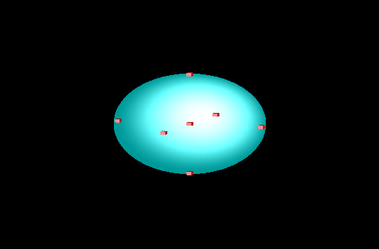
Pyramid - Simulation Object
FDTD MODE DGTD CHARGE HEAT FEEM
This page describes a pyramid object. Pyramids can be configured to half flat tops and/or flat bottoms, and either narrow or expand in the vertical z direction.
Geometry tab
- X, Y, Z: The center position of the object
- X SPAN BOTTOM, X SPAN TOP: X bottom, top span of the object
- Y SPAN BOTTOM, Y SPAN TOP: Y bottom, top span of the object
- Z MIN, Z MAX: Z min, Z max position
- Z SPAN: Z span of the object
Material tab
The material options are as follows:
- MATERIAL: This field can be set to any material included in the material database. It is possible to include new materials in the database, or edit the materials already included. See the material database section for more information.
- OVERRIDE MESH ORDER FROM MATERIAL DATABASE: Select to override the mesh order from the material database and manually set a mesh order. The mesh order is used by the simulation engine to select which material to use when two materials overlap. See the mesh order (optical) or mesh order (electrical) section for more details.
- MESH ORDER: Set the mesh order in this field if the OVERRIDE MESH ORDER FROM MATERIAL DATABASE option is selected. If the option is not selected, the field displays the material's default mesh order from the database. For example, a material of mesh order 1 will take precedence over a material of mesh order 2.
The following only applies to MODE and FDTD:
If <Object defined dielectric> is selected, then the INDEX property must be set.
- INDEX: The refractive index of the structure, when the material type is <Object defined dielectric>. The index must be greater than one.
-
-
- Anisotropic index: To specify an anisotropic refractive index, use a semicolon to separate the diagonal xx,yy,zz indices. Eg. 1;1.5;1
- Spatially varying index: It is possible to specify a spatially varying refractive index by entering an equation of the variables x,y,z in this field. Eg. 2+0.1*x will create an object where the refractive index increases in the X direction. The units of the spatial variables (x,y,z) must be set with the 'INDEX UNITS' property described below. The variables x,y,z will be zero in the center of the object. When using an equation in this field, consider using a mesh override region to control the simulation mesh size. For more information on entering equations, see the Equation interpreter section.
-
- INDEX UNITS: Only relevant when specifying a spatially varying equation in the INDEX properly described above. Specify the units (nm, um, m) of the x,y,z position variables.
- GRID ATTRIBUTE NAME: Enter the name of the grid attribute that applies to this object, see the grid attribute section
The following only applies to CHARGE, HEAT, FEEM, DGTD:
If the material chosen from the drop down menu is a binary alloy consisting of two semiconductors, then there will be an additional property, namely, the "composition fraction" to set as well.
- COMPOSITION FRACTION: This is x, the fraction of the semiconductor in the alloy. x can either take a fixed value or vary.
The user can see which semiconductor has fraction x and which has fraction (1-x) shown in a line above this drop down menu.
- FIXED: This means that fraction x will be a constant value between 0 and 1.
- LINEAR X/Y/Z: This means that the composition fraction x will vary as a function x or y or z. In this case, user can specify the min and max fraction values for the min and max spatial points and the fraction will be interpolated linearly in between. x,y,z here are those of the unrotated object. x,y,z are local to the object.
- EQUATION: The user can enter an equation for the fraction that varies with u,v and w. u is (x-x0), v is (y-y0) and w is (z-z0) where x0, y0 and z0 are the center coordinates of the object. This means that u,v and w are local to the object.
Rotation tab
Rotate objects by setting the following variables:
- FIRST, SECOND, THIRD AXES: Select rotation axis. Up to three different rotations can be applied.
- ROTATION 1,2,3: The rotation of the object in a clockwise direction about each axis, measured in degrees.
Graphical Rendering tab
The graphical rendering tab is used to change how objects are drawn in the layout editor. The options are:
- RENDER TYPE: The options for drawing the objects are detailed or wireframe. Detailed objects are shaded and their transparency can be set using OVERRIDE COLOR OPACITY FROM MATERIAL DATABASE.
- DETAIL: This is a slider which takes values between 0 and 1. By default it is set to 0.5. Higher detail shows more detail, but increases the time required to draw objects. This setting has no effect on the simulation.
- OVERRIDE COLOR OPACITY FROM MATERIAL DATABASE: When unselected the opacity is determined from the material database. When selected, you can specify a value for ALPHA between 0 (transparent) and 1 (opaque) for the object, depending on how transparent you want the object to be.
Planar solid - Simulation Object
FDTD MODE DGTD CHARGE HEAT FEEM
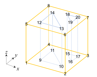
The planar solid object behaves somewhat like the polygon structure, but generalized to 3D. The object vertices cannot be set via the GUI; a script command must be used. The image below shows how a facet is defined to denote positive or negative spaces. In the shape below one facet comprises of two paths : p1=[1,3,2,5,4] , p2=[16,17,18,19].

Setting the vertices of the polygon object
The vertices of the planar solid object can be edited using scripting by two methods:
- Specifying the vertices as a cell array.
- Specifying the vertices as a matrix.
For complex shapes, one can use multiple primitives and set the mesh orders of overlapping structures to achieve the desired shape, but using the planar solid primitive allows you to use just one object to implement complex shapes.
Geometry tab
- X, Y, Z: The center position of the object
Material tab
The material options are as follows:
MATERIAL: This field can be set to any material included in the material database. It is possible to include new materials in the database, or edit the materials already included. See the material database section for more information.
- OVERRIDE MESH ORDER FROM MATERIAL DATABASE: Select to override the mesh order from the material database and manually set a mesh order. The mesh order is used by the simulation engine to select which material to use when two materials overlap. See the mesh order (optical) or mesh order (electrical) section for more details.
- MESH ORDER: Set the mesh order in this field if the OVERRIDE MESH ORDER FROM MATERIAL DATABASE option is selected. If the option is not selected, the field displays the material's default mesh order from the database. For example, a material of mesh order 1 will take precedence over a material of mesh order 2.
The following only applies to MODE and FDTD:
If <Object defined dielectric> is selected, then the INDEX property must be set.
- INDEX: The refractive index of the structure, when the material type is <Object defined dielectric>. The index must be greater than one.
-
-
- Anisotropic index: To specify an anisotropic refractive index, use a semicolon to separate the diagonal xx,yy,zz indices. Eg. 1;1.5;1
- Spatially varying index: It is possible to specify a spatially varying refractive index by entering an equation of the variables x,y,z in this field. Eg. 2+0.1*x will create an object where the refractive index increases in the X direction. The units of the spatial variables (x,y,z) must be set with the 'INDEX UNITS' property described below. The variables x,y,z will be zero in the center of the object. When using an equation in this field, consider using a mesh override region to control the simulation mesh size. For more information on entering equations, see the Equation interpreter section.
-
- INDEX UNITS: Only relevant when specifying a spatially varying equation in the INDEX properly described above. Specify the units (nm, um, m) of the x,y,z position variables.
- GRID ATTRIBUTE NAME: Enter the name of the grid attribute that applies to this object, see the grid attribute section
The following only applies to CHARGE, HEAT, FEEM, DGTD:
If the material chosen from the drop down menu is a binary alloy consisting of two semiconductors, then there will be an additional property, namely, the "composition fraction" to set as well.
- COMPOSITION FRACTION: This is x, the fraction of the semiconductor in the alloy. x can either take a fixed value or vary.
The user can see which semiconductor has fraction x and which has fraction (1-x) shown in a line above this drop down menu.
- FIXED: This means that fraction x will be a constant value between 0 and 1.
- LINEAR X/Y/Z: This means that the composition fraction x will vary as a function x or y or z. In this case, user can specify the min and max fraction values for the min and max spatial points and the fraction will be interpolated linearly in between. x,y,z here are those of the unrotated object. x,y,z are local to the object.
- EQUATION: The user can enter an equation for the fraction that varies with u,v and w. u is (x-x0), v is (y-y0) and w is (z-z0) where x0, y0 and z0 are the center coordinates of the object. This means that u,v and w are local to the object.
Rotation tab
Rotate objects by setting the following variables:
- FIRST, SECOND, THIRD AXES: Select rotation axis. Up to three different rotations can be applied.
- ROTATION 1,2,3: The rotation of the object in a clockwise direction about each axis, measured in degrees.
Graphical Rendering tab
The graphical rendering tab is used to change how objects are drawn in the layout editor. The options are:
- RENDER TYPE: The options for drawing the objects are detailed or wireframe. Detailed objects are shaded and their transparency can be set using OVERRIDE COLOR OPACITY FROM MATERIAL DATABASE.
- DETAIL: This is a slider which takes values between 0 and 1. By default it is set to 0.5. Higher detail shows more detail, but increases the time required to draw objects. This setting has no effect on the simulation.
- OVERRIDE COLOR OPACITY FROM MATERIAL DATABASE: When unselected the opacity is determined from the material database. When selected, you can specify a value for ALPHA between 0 (transparent) and 1 (opaque) for the object, depending on how transparent you want the object to be.
Scripting example
Here we show an example script for constructing a cube with two planar holes using the planar solid primitive.
# Select method of formatting data used to create the object
method_type = 1;

# Specify vertex locations (Refer to the figure above)
vtx = [0,0,0;
       1,0,0;
       1,1,0;
       0,1,0;
       0,0,1;
       1,0,1;
       1,1,1;
       0,1,1;
       0.25,.25,0;
       0.8,.25,0;
       0.25,.8,0;
       0.25,.25,1;
       0.8,.25,1;
       0.25,.8,1;
       0.5,.8,0;
       0.8,.5,0;
       0.8,.8,0;
       0.5,.8,1;
       0.8,.5,1;
       0.8,.8,1]*1e-6;

# Data format method 1: facet table as cell array
a = cell(12);

for (i = 1:12) {
  if ((i == 1) | (i == 6)) {
    a{i} = cell(3);
  } else {
    a{i} = cell(1);
  }
}

a{1}{1} = [1,4,3,2];   # bottom facet has two holes
a{1}{2} = [9,10,11];   # first hole (orientation auto-corrected)
a{1}{3} = [15,16,17];  # second hole
a{2}{1} = [1,5,8,4];   # x min
a{3}{1} = [1,2,6,5];   # y min
a{4}{1} = [2,6,7,3];   # x max
a{5}{1} = [3,4,8,7];   # y max
a{6}{1} = [5,6,7,8];   # top face has two matching holes to bottom
a{6}{2} = [14,13,12];
a{6}{3} = [20,19,18];
a{7}{1}  = [10,9,12,13]; # inner faces of holes
a{8}{1} = [11,10,13,14];
a{9}{1} = [9,11,14,12];
a{10}{1} = [16,15,18,19];
a{11}{1} = [15,17,20,18];
a{12}{1} = [17,16,19,20];

if (method_type == 1) {
  addplanarsolid(vtx,a);
}

# Data format method : facet table as matrix
else {
  b = matrix(4,3,12);  # max four points per polygon, max 3 polygon per facet
  for (i = 1:12) {
    for (ipol = 1:length(a{i})) {
      fpoly = a{i}{ipol};
      for (j = 1:length(fpoly)) {
        b(j,ipol,i) = fpoly(j);
      }
    }
  }
  addplanarsolid;
  set('vertices',vtx); # must be done first
  set('facets',b);
}
2D Rectangle - Simulation Object
FDTD MODE DGTD CHARGE HEAT FEEM
This is a true 2D rectangle (or a surface object), which has no thickness in the normal direction. This object can be used with the graphene model using the surface conductivity approach.
Geometry tab
- Surface normal: X, Y or Z. This is the surface normal of the 2D rectangle. When a direction of the normal is selected, the 2D rectangle object will be rotated accordingly and the corresponding direction options to specify span and min/max values will be grayed out. The 2D rectangle object has no thickness.
- X, Y, Z: The center position of the object
- X MIN, X MAX: X min, X max position
- Y MIN, Y MAX: Y min, Y max position
- Z MIN, Z MAX: Z min, Z max position
- X SPAN, Y SPAN, Z SPAN: X, Y, Z span of the object
Material tab
The material options are as follows:
- MATERIAL: The material assigned to a 2D rectangle is filtered. It can only be a dielectric with fixed index or a graphene material type.
- OVERRIDE MESH ORDER FROM MATERIAL DATABASE: Select to override the mesh order from the material database and manually set a mesh order. The mesh order is used by the simulation engine to select which material to use when two materials overlap. See the mesh order (optical) or mesh order (electrical) section for more details.
- MESH ORDER: Set the mesh order in this field if the OVERRIDE MESH ORDER FROM MATERIAL DATABASE option is selected. If the option is not selected, the field displays the material's default mesh order from the database. For example, a material of mesh order 1 will take precedence over a material of mesh order 2.
Note:Mesh order between 2D and 3D objects
- 2d objects always take priority over 3d objects. For example, a 3d cylinder overlapping a 2d rectangle will not create a hole in the 2d rectangle, regardless of their mesh order.
- 2d objects respect mesh order among themselves. For example, a 2d rectangle with RLC overlapping a 2d polygon with PEC. The material of the overlap is determined according to mesh orders.
- Please refer to the Understanding mesh order for overlapping objects for further information.
INDEX: The refractive index of the structure, when the material type is <Object defined dielectric>. The index must be greater than one.If <Object defined dielectric> is selected, then the INDEX property must be set.
-
-
- Anisotropic index: To specify the anisotropy, use the "Surface normal" option in the geometry tab.
- Spatially varying index: This is not supported in this 2D rectangle object.
-
- INDEX UNITS: Only relevant when specifying a spatially varying equation in the INDEX properly described above. Specify the units (nm, um, m) of the x,y,z position variables.
- GRID ATTRIBUTE NAME: Enter the name of the grid attribute that applies to this object, see the grid attribute section
Rotations tab
Rotate objects by setting the following variables:
- FIRST, SECOND, THIRD AXES: Select rotation axis. Up to three different rotations can be applied.
- ROTATION 1,2,3: The rotation of the object in a clockwise direction about each axis, measured in degrees.
| Note: Axis rotation This object does not support arbitrary angle of rotation on the non-normal axis. For example, with z axis being the normal, rotation of 30 degrees along z is allowed. However, rotation of 30 degrees along x or y axis is not allowed. Also note, the "Surface normal" option in the "Geometry tab" also rotates the object accordingly. |
Graphical Rendering tab
The graphical rendering tab is used to change how objects are drawn in the layout editor. The options are:
- RENDER TYPE: The options for drawing the objects are detailed or wireframe. Detailed objects are shaded and their transparency can be set using OVERRIDE COLOR OPACITY FROM MATERIAL DATABASE.
- DETAIL: This is a slider which takes values between 0 and 1. By default it is set to 0.5. Higher detail shows more detail, but increases the time required to draw objects. This setting has no effect on the simulation.
- OVERRIDE COLOR OPACITY FROM MATERIAL DATABASE: When unselected the opacity is determined from the material database. When selected, you can specify a value for ALPHA between 0 (transparent) and 1 (opaque) for the object, depending on how transparent you want the object to be.
2D Polygon - Simulation Object
FDTD MODE DGTD CHARGE HEAT FEEM
The object is defined in 2d surface and does not have thickness in the surface-normal direction. It can be used with 2D materials such as graphene, PEC and sampled 2d data.
Note: 2d objects always take priority over 3d objects when it comes to mesh orders. Please refer to the Understanding mesh order for overlapping objects for further information.
Here are some of the example structures that can be created using a 2D polygon object. To create any one of these structures, open the 2d_poly_examples.lsf and run the corresponding part of the script.

Geometry tab
- X, Y, Z: The center position of the object
Setting the vertices of the polygon object
The vertices of the polygon object can be edited by
- moving them with the mouse,
- manually editing the x,y location of each vertex in the polygon property editor,
- script command
For complex shapes, scripting in the structure group is usually best. Once the script has calculated the x,y vertex positions, they can be loaded into the polygon object with a single set("vertices",V); command. For example, use the following code to create an octagon shaped object.
# octagon properties
n_sides=8;
r=1e-6;

# x,y position of each corner
theta=linspace(0,360,n_sides+1);
theta=theta(1:n_sides);
x=r*cos(theta*pi/180);
y=r*sin(theta*pi/180);

# combine x,y into one vertices matrix
V=matrix(n_sides,2);
V(1:n_sides,1)=x(1:n_sides);
V(1:n_sides,2)=y(1:n_sides);

# add polygon object and set the vertices
addpoly;
set("vertices",V);
Getting and modifying polygon vertices
To get the polygon vertices, use the following command. The vertices will be returned in an Nx2 matrix. The columns of this matrix correspond to the X, Y positions of each vertex.
V=get("vertices");
?size(V);
To modify a polygon vertex, you must get the vertices matrix, modify the vertex matrix as desired, then re-apply it to the polygon object:
V=get("vertices");
V(1,1)=V(1,1)+1e-6; # change the x position of the first vertex by 1um.
set("vertices",V);
Material tab
The material options are as follows:
- MATERIAL: The material assigned to a 2D polygon is filtered. It can only accept graphene, PEC(perfect electric conductor), sampled 2d data material types.
- OVERRIDE MESH ORDER FROM MATERIAL DATABASE: Select to override the mesh order from the material database and manually set a mesh order. The mesh order is used by the simulation engine to select which material to use when two materials overlap. See the mesh order (optical) or mesh order (electrical) section for more details.
- MESH ORDER: Set the mesh order in this field if the OVERRIDE MESH ORDER FROM MATERIAL DATABASE option is selected. If the option is not selected, the field displays the material's default mesh order from the database. For example, a material of mesh order 1 will take precedence over a material of mesh order 2.
Note:Mesh order between 2D and 3D objects
- 2d objects always take priority over 3d objects. For example, a 3d cylinder overlapping a 2d rectangle will not create a hole in the 2d rectangle, regardless of their mesh order.
- 2d objects respect mesh order among themselves. For example, a 2d rectangle with RLC overlapping a 2d polygon with PEC. The material of the overlap is determined according to mesh orders.
- Please refer to the Understanding mesh order for overlapping objects for further information.
Rotations tab
Rotate objects by setting the following variables:
- FIRST, SECOND, THIRD AXES: Select rotation axis. Up to three different rotations can be applied.
- ROTATION 1,2,3: The rotation of the object in a clockwise direction about each axis, measured in degrees.
| Note: Axis rotation This object does not support an arbitrary angle of rotation on the non-normal axis. For example, with z axis being the normal, rotation of 30 degrees along z is allowed. However, rotation of 30 degrees along x or y axis is not allowed. Also note, the "Surface normal" option in the "Geometry tab" also rotates the object accordingly. |
Graphical Rendering tab
The graphical rendering tab is used to change how objects are drawn in the layout editor. The options are:
- RENDER TYPE: The options for drawing the objects are detailed or wireframe. Detailed objects are shaded and their transparency can be set using OVERRIDE COLOR OPACITY FROM MATERIAL DATABASE.
- DETAIL: This is a slider which takes values between 0 and 1. By default it is set to 0.5. Higher detail shows more detail, but increases the time required to draw objects. This setting has no effect on the simulation.
- OVERRIDE COLOR OPACITY FROM MATERIAL DATABASE: When unselected the opacity is determined from the material database. When selected, you can specify a value for ALPHA between 0 (transparent) and 1 (opaque) for the object, depending on how transparent you want the object to be.
Complex structures:
Structure group to create arrays of objects
This page provides a structure group that can be used to create arrays of other objects. The simulation file usr_array_structure_group.fsp contains a structure group that will create an array of objects that are placed within the group.
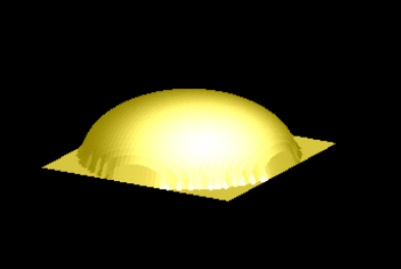
For example, suppose we want to create an array of hemispheres.
| Step 1 Create the structure that you want to array. In this case, we have created a hemisphere using the surface object. If your structure is composed of more than one primitive, remember to group the primitives together. |
| ||||||
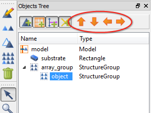
| Step 2 Change the name of your structure to 'object'. Move your structure named 'object' into the array_group. This is most easily accomplished with the reposition arrows (circled in the screenshot to the right). |
| ||||||
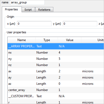
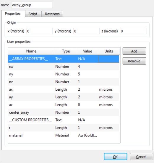
| Step 3 Setup the array structure group as required.
It's possible to add custom properties to this object to modify each instance of the original object. In this example, we have radius and material properties to adjust the hemisphere. |
| ||||||
| Step 4 The array structure group will automatically create an array of the objects. |
|
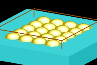
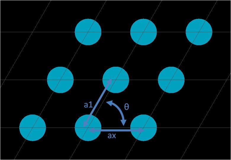
For another example of a structure group that can be used to create arrays, see the Structure groups page. This page provides a detailed description of how to create your the 2D array object shown below.
Tips for creating structures with rounded corners
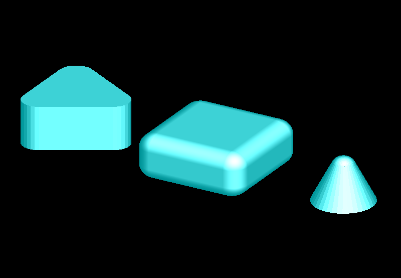
This section describes how to create objects with rounded corners. The example file here was created in FDTD, but these structures can be found in the component libraries of other products as well.
Creating objects with rounded corners
Method 1:
Objects with rounded corners can be created with the polygon object. The simulation file usr_round_corners.fsp contains an n-sided equilateral shape with rounded corners created using the polygon primitive and then extruding. This object can also be accessed via the object library. By default, one corner of the object always points in the +X direction. The rotation tab of the structure group can be used to rotate the object.
Method 2:
Rounded objects can also be created using a combination of rectangles, spheres and extruded circles (tubes). Using the structure group script, the above all-rounded rectangular prism can be produced and easily modified.
Note: Continuous slope
Sometimes, adding a sphere to round a part of the structure can be tricky. The sphere must be positioned such that there is a continuous slope at the interface between it and the structure. Often, satisfying this criteria has the unwanted effect of the sphere protruding out of the sides when it shouldn't. To fix this, we use a revolved custom object with a spherical equation, rather than a sphere. This allows us to specify the domain of the equation (x-min and x-max) and thus, limit the section of the sphere that we want. The rounded cone is a good example of this problem.
Tips for creating waveguide bends using the path object
This section describes how to create various waveguide bends using the waveguide object. The path of the waveguide is a Bezier curve, which is defined by a set of points, called 'poles.' Further detail on Bezier curve can be found on the ' Structures - Waveguide' page.
The example file, usr_waveguide_bends.fsp, contains an s-bend and a Y-branch, which can be used to build more complex structures such as cascaded y-branches and directional couplers.
Creating an S-bend
The s-bend waveguide can be created by specifying the poles in the 'edit waveguide' window. The red dots in the image below corresponds to the poles in the table on the right. The example s-bend can be located in the usr_waveguide_s_bend.fsp.
If only two poles are specified, a straight waveguide is formed.
|
|
|
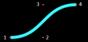
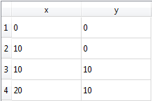
Creating a Y-branch
Using the straight and the s-bend waveguides as building blocks, a Y-branch structure group as shown below can be created. The group contains two s-bend as well as three rectangles. The dimensions of the waveguides (x1, x2, y2) can be parametrized and a script in the structure group can be used to build the structure automatically. This is a good example of a parent structure script modifying child structure scripts.
|
|
|
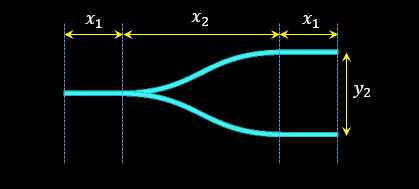
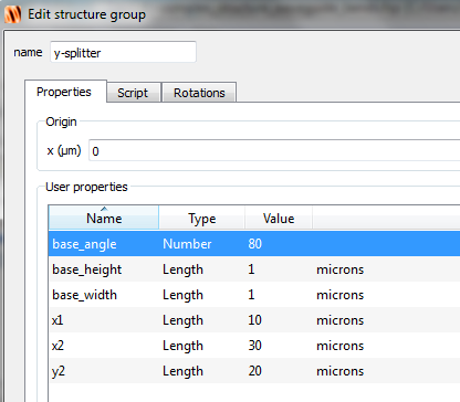
The following script is used in the 'script' section of the structure group:
select("straight_in");
set("poles",[0,0;x1,0]);

select("straight_out1");
set("poles",[x1+x2,y2/2;2*x1+x2,y2/2]);

select("straight_out2");
set("poles",[x1+x2,-y2/2;2*x1+x2,-y2/2]);

select("s_bend_1");
set("poles",[x1,0;x1+x2/2,0;x1+x2/2,y2/2;x1+x2,y2/2]);

select("s_bend_2");
set("poles",[x1,0;x1+x2/2,0;x1+x2/2,-y2/2;x1+x2,-y2/2]);
Note: Reference points
The pole points are defined at the center of the waveguide cross section. The x1, x2, and y2 in the Y-splitter example are all measured with respect to the corresponding pole points.
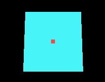
Tips for adding sidewall angles to simulation objects
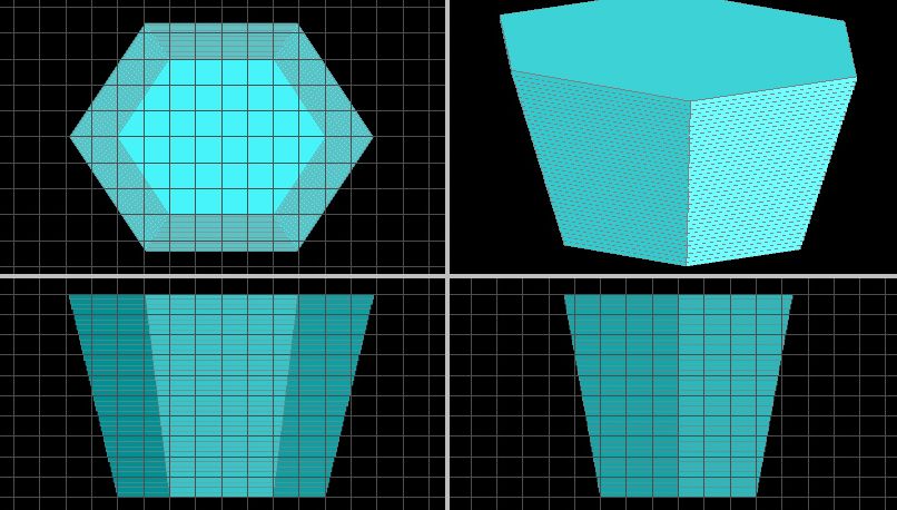
This section provides a script file that can be used to extrude any polygon with a desired sidewall angle. The example file here was created in FDTD, but these structures can be found in the component libraries of other products as well.
Extruding a polygon with a sidewall angle
FDTD supports extruded polygons in three dimensions, but the sidewalls are always vertical. A non-vertical sidewall angle can be created by using a series of polygons that increase or decrease in scale as a function of height.
The above figure shows an extruded polygon that can be constructed by inserting a polygon in a simulation file, selecting the polygon and running the script usr_extrude_poly.lsf.
This script uses one method to scale the vertices as a function of depth while retaining the original vertex shape at all depths. The script can be modified by users who are interested in other algorithms for determining the shape of an extruded structure with non-vertical sidewalls.
| Note: Simulation times when using large numbers of primitives. The simulation time is not affected by the number of primitives used to create the physical structures. The meshing time (which occurs before the simulation begins) will increase with the number of primitives used. However, since the meshing time is normally much less than the simulation time, this will not have a significant effect on the total time. |
Tips for creating spiral and helix geometries
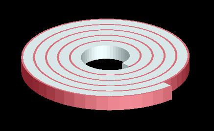
The helix and spiral objects can be found in the Object library Structures category under the "Uncategorized structures" heading. This section describes how these two types of spiral objects are created.
Spiral
The spiral is created with a series of polygon primitives. In this example, each ring of the spiral is one polygon object.
The top figure above shows the spiral structure group object from usr_spiral.fsp. Spiral parameters such as radius, types of the two materials that make up the spiral, and number of turns can be modified by editing the user properties of the group.
Helix
The helix object is created with a series of thin cylinders. The second figure above shows a helix structure group object from usr_helix.fsp. Helix parameters such as radius and number of turns can be modified by editing the user properties of the group.
| Note: Simulation times when using large numbers of primitives. The simulation time is not affected by the number of primitives used to create the physical structures. The meshing time (which occurs before the simulation begins) will increase with the number of primitives used. However, since the meshing time is normally much less than the simulation time, this will not have a significant effect on the total simulation time. |
Conical helix
With the Helix structure group, user may change the start and end radius of the helix to make it like a cone. User may want to pay attention to the situation when the "fiber radius" is comparable to the "end radius" that makes the structure distorted. In that case, changing the fiber radius or other parameters may need to be considered.

Tips for adding surface roughness to structures
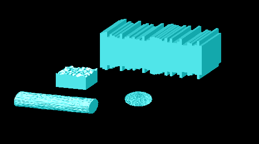
This section describes how to create objects with surface roughness.
Simple roughness example
The structure group named surface roughness simple which is located in usr_surface_roughness.fsp shows a simple technique for adding surface roughness to a ridge waveguide. Rather than creating the structure from a single rectangle, it is composed of many thin slices, each with a random variance in width.
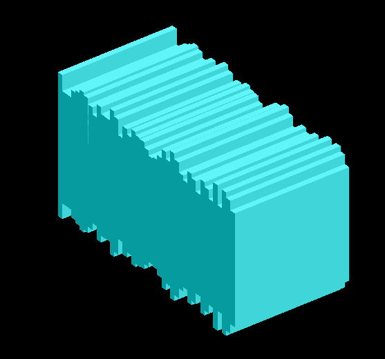
Advanced surface roughness
The structure group named surface roughness advanced which is located in usr_surface_roughness.fsp shows a more advanced surface roughness model. In this case, the roughness is characterized by a specified sigma RMS (s) and correlation length (Lc). These quantities are related to the correlation function by
〈H(r)H(r+δ)〉=σ2e(−(δLc)2)
The roughness is generated creating a matrix of uniform random numbers in k space. The high frequency components are removed, and the resulting values are transformed back to real space.
|
|
|
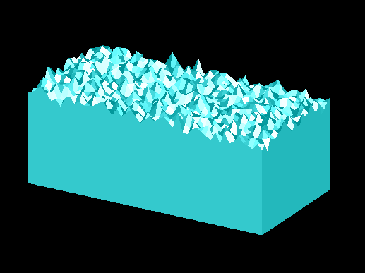
In this case, a single import object (surface option) is used to define the entire object, rather than building the surface from many simple primitives like the previous example. The upper surface of this object is defined by a 2D matrix containing the surface height as a function of x and y.
The set up script initially fills the surface matrix in K-space with uniform random numbers. A filter is applied to remove all high frequency components. The matrix is transformed back into real space, where the amplitude is corrected. The import object is then added to the simulation.
An example of a ridge waveguide with rough sidewalls based on this technique can be found in rough_waveguide.fsp.
The surface roughness plot can also be applied to wrap around a wire. In this structure group, each slice of x containing the array of height adjustments (y) is used to perturb points in a circle. When stacked, just like the rough ridge waveguide example from above, it creates a continuous structure with a rough exterior.
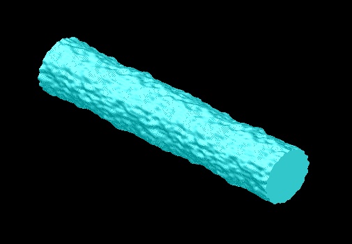
Note that the detail setting for the graphical rendering is increased because this is a complex surface. A higher detail setting makes the surface look better in the CAD editor, but will make the drawing slow if you have many complex surfaces with many data points. The detail setting has no effect on the actual meshing of the structure.
Tips for creating a 3D contour path object
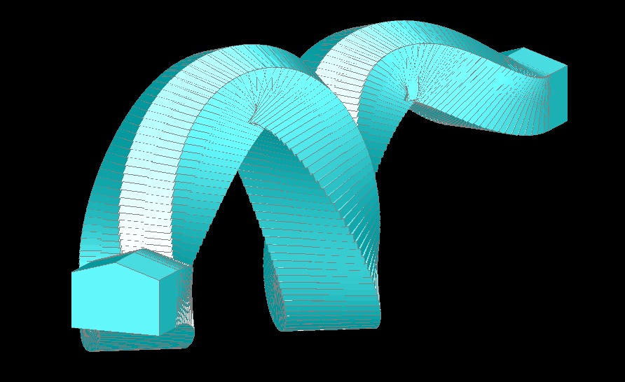
This section describes how to create an arbitrary 3D contour with a polygonal cross section.
Creating an arbitrary 3D contour
This example uses a large number of polygon objects to create an arbitrary 3D contour. The user defines an arbitrary line contour path in 3 dimensions, and a polygonal cross sectional shape. The structure is created from sections of rotated and extruded polygons. The user can increase the number of sections used by increasing the number of sample points of the contour. The above structure shows the contour structure group from usr_contour.fsp. Only user properties and the first portion of the setup script in the structure group defining the cross section and contour path should be modified. For example, a simpler structure could be created by replacing the lines defining z:
z = matrix(N_sections);
z(1) = 0;
z(N_sections) = 0;
z(2:N_sections-1) = 5e-6*sin(phi)*sin(phi/4);
with
z=0;
The structure is now bound to z=0 as shown below. Contour paths can be defined analytically, or could be read from a text file with the readdata script command.
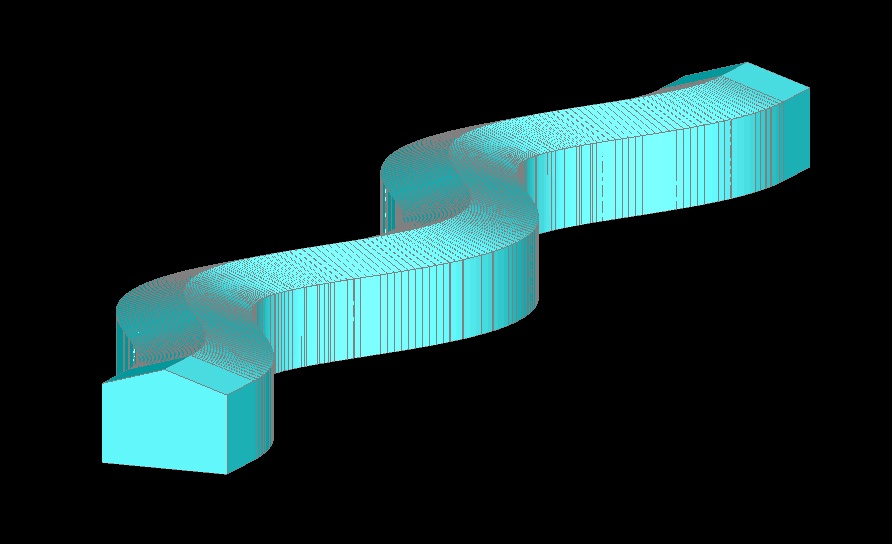
Layer builder - Simulation object
FDTD MODE DGTD CHARGE HEAT FEEM
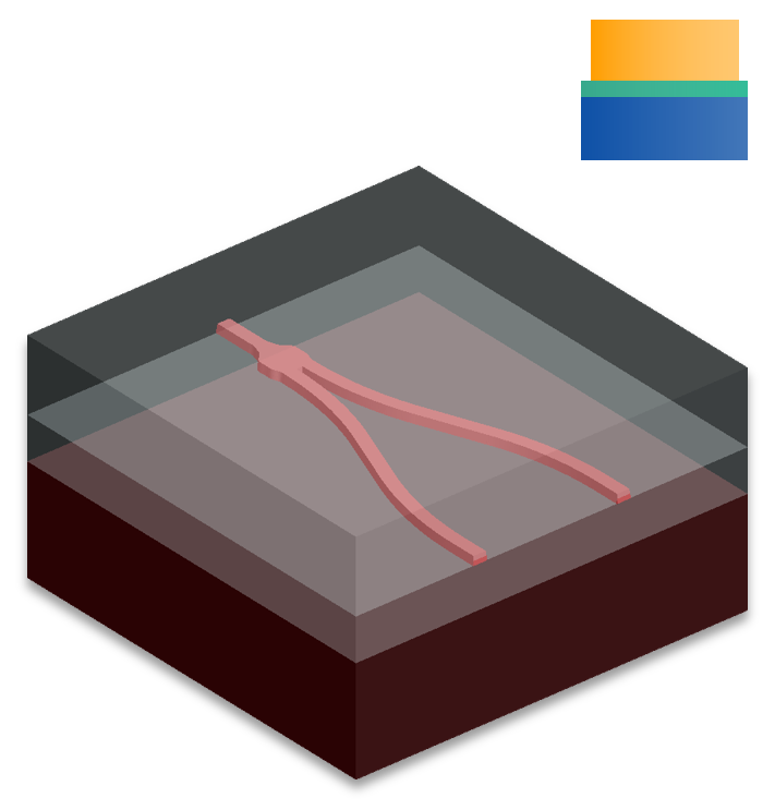
The Layer builder button adds a layer builder object. It can be used to construct a layered structure consisting of planar unpatterned layers as well as patterns imported from a GDS file. Patterns can also be defined via Lumerical script. This tool allows you to:
- Easily change the position, ordering, and thickness of each layer.
- Translate the position of the patterning within a layer.
- Add sidewall angles to patterns.
- Export and import the layer configuration, including material data, as a process file (.lbr).
Compared to the GDS import option described in GDSII - Import and export, the Layer Builder offers a more complete solution because it can combine the pattern information from GDS files with the vertical layer information from a process file. This functionality can be very useful, for example, in custom design of components using a particular foundry process.
| Note: Limitations of layer-builder
|
The following sections explain how to set up a layer builder object, illustrating each step with a simple example of a silicon y-branch structure both from scratch and from an existing process file:
- All the setup operations can be done either from the GUI or from script. It is recommended to become familiar with the GUI first (see Setting up from the GUI).
- For a complete list of script commands and references to their specific documentation see the section Setting up from script.
- Finally, some additional considerations for configuring a layer builder object are explained in the Appendix section.
Setting up from the GUI
This section covers the following topics:
- Add and edit a layer builder object
- Set up the pattern geometry
- Add and edit process layers
- Set up the background geometry
- View the final structure in the CAD
Add and edit a layer builder object
Open a new simulation file, add a new layer builder object by clicking on the
![]()
button and open the Edit window for the new object.
Set up the pattern geometry
| NOTE: In the GUI, the pattern geometry can only be defined by importing a GDS file. The alternative is to define the geometry via script by providing the polygon vertices directly to the layer builder object, as explained in Setting up from script. |
In the Layout section of the Layer Builder Edit window, you can:
- Import GDS file. Note that the file is loaded once when this button is used. The GDS file is not reloaded automatically in the future if there are changes; therefore, you must reload the file if it has changed and you want to update the geometry in the layer builder object accordingly. The name and location of the GDS file at the time it was imported is shown in the GDS file box.
- Reload GDS file with the name and location specified in the GDS file box. It is possible to perform this operation directly from the layer builder object by right-clicking on it in the Objects Tree and selecting “Reload GDS file”. If the file name or location have changed, you need to use the Import GDS file button instead.
- Remove geometry to clean the pattern geometry saved in the layer builder object. This will also clear the GDS file box.
- Select a GDS cell in the GDS file to be imported.
- Choose the GDS sidewall angle position reference applied to the GDS patterns in all the process layers. The XY cross-section of the structure will match with the GDS pattern at this position. Options are middle (default), top or bottom of the layer. For more information on sidewall angle see Add and edit process layers.
- Export a GDS file with the pattern geometry and layer numbers currently saved in the layer builder object.
Note that a layer builder object can only load data from a single cell from a single GDS file. If you need to import multiple cells from one or multiple GDS files into a single simulation, you need to create a layer builder object for each of them.
Example
Download the y_500.gds file from the Associated Files section above and click on the Import GDS file button to load it into the layer builder object. This GDS file has only one cell, as shown below:
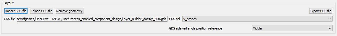
Add and edit process layers
| NOTE: If you already have a process file (.lbr), you can load it with the Import process file button. This will automatically load all the process layer information from the file into the layer list, which you can then edit if needed, as explained here. If no changes to the layer list are required, you can skip this section and go to Set up the background geometry after importing the process file. |
In the Layers section of the Layer Builder Edit window, you can:
- Add or Remove process layers.
- Change the position of a process layer in the list by selecting the layer and using the Up and Down buttons. The order of the layers in the list is important to determine their priority correctly when they overlap, as explained in Priority of overlapping process layers.
- Enable or disable the objects in the simulation that correspond to a process layer by checking or unchecking the corresponding tick box in the enabled column.
- Define a name for the process layer.
- Select the corresponding GDS layer number. Note that multiple process layers can be associated with a single GDS layer; i.e. the mapping between the two types of layers is not necessarily one-to-one and it depends on the process definition:
- The list of available GDS layers is shown if a GDS file has been imported beforehand.
- Otherwise, use the option "<Other>" to specify a GDS layer. You can also use this option to specify a GDS layer using Boolean operations:
- Use not( ) to generate the negative of the pattern (i.e. the background minus the pattern).
- Use or to generate all patterns corresponding to the selected layer numbers.
- Use and to generate the overlap of the patterns corresponding to the selected layer numbers.
- Use xor to generate the patterns corresponding to the selected layer numbers minus their overlapping areas.
- Specify the start position of the layer, which is the z position where the extrusion of the layer starts, in coordinates relative to the origin of the layer builder object (defined in global simulation coordinates in the Background geometry section). By default, the start position of a new layer is “Auto”, which means that it will be right on top of the previous layer in the list; for the first layer, “Auto” sets the start position to the origin of the layer builder object.
- Provide the thickness of each process layer. It can be a positive or negative real number depending on the direction the layer extends from the start position defined above:
- Upwards (positive z direction) for positive values.
- Downwards (negative z direction) for negative values.
- Define the GDS pattern and background material. This can be any material from the Material database or an “Object defined dielectric”. The material data can be saved in the process file as explained in Exporting and importing material data.
- Choose a type of process step:
- Background: No pattern from GDS (or its negative) is used; therefore, “pattern material” is disabled and “background material” must be specified. A rectangle with the position and span defined in the Background geometry section is added as the process layer.
- Grow: The GDS pattern is extruded from the specified start position. “Pattern material” must be specified but “background material” is optional. If "background material" is specified, a rectangle with the position and span defined in the Background geometry section is added to set the background material surrounding the extruded pattern.
- Add sidewall angle to the pattern in a process layer. The sidewall angle can take values in the range (0,180) degrees:
- = 90 degrees (default): perfectly vertical wall.
- < 90 degrees: the pattern at the bottom of the process layer is larger than at the top.
- > 90 degrees: the pattern at the bottom of the process layer is smaller than at the top.
- Add a pattern growth delta to a process layer. This delta is a uniform shift of the patterns outwards (if positive) or inwards (if negative). It can be used to capture uniform under-etch or over-etch due to fabrication. Note that even when a pattern growth delta has been applied to a layer, only the original pattern will be exported to the GDS file.
- Import and export your process layer configuration as a process file (.lbr). Once you have configured your list of layers, you can save it in a process file that can be loaded in any layer builder object. It is possible to save the material data (e.g. sampled data, fit parameters, etc.) in the process file by checking the option “export materials”; otherwise, only the material name will be saved in the process file. See Exporting and importing material data for more information.
Example
For the y-branch example, add five layers in the Edit window of the Layer Builder and configure them as shown below:

Alternatively, you can load the example process file lumerical_foundry_process_file.lbr from the Associated Files section.
Note the following:
- For "BOX" the "Auto" option can be used for start position since this process layer is stacked on top of "Si_Substrate".
- For "Si_CoreStripWG" and "Si_SlabRibWG" the start position is set to 0 because the bottom of these process layers coincides with the bottom of "TOX".
- For "Si_Substrate" the start position is set to -2 um and the thickness to -10 um so that the process layer extends downwards starting at the bottom of "BOX".
- The process of "Si_Substrate", "BOX", "TOX" are set to "Background" since they have no patterning. Note that the layer number and pattern material fields become disabled.
- The GDS layer 1:1 used in "Si_SlabRibWG" is not present in the example GDS file and so the layer number is highlighted in yellow.
- If you want to use the negative of the GDS pattern in "Si_CoreStripWG", you can use not(1:0) as the layer number.
Set up the background geometry
In the Background geometry section of the Layer builder Edit window, you can:
- Define the (x, y, z) position of the origin of the layer builder object in global simulation coordinates. This origin also defines the center of the background geometry in the XY plane. Note that the z position corresponds to the bottom of layers if the start position of all the layers is “Auto”.
- Set the x and y span of the background geometry for all layers, which should be large enough for the GDS patterns to fit inside.
- Specify the base mesh order (default is 2), which is the lowest mesh order a structure inside the layer builder object can have. This setting can be used to set the priority of the structures inside the layer builder object relative to other simulation objects when overlap occurs, as explained here.
- Set x and y positions of the origin of the GDS pattern reference frame in coordinates of the layer builder object. You can choose from pre-set options in the drop-down menu to align the origin of the GDS coordinate system with the origin or the corners of the background geometry; it is also possible to specify custom (x, y) coordinates.
- A preview is automatically generated showing the GDS pattern (blue box with the origin of the GDS reference frame marked by a cross) and the background geometry (red box).
Example
In the y-branch example configure the background geometry as shown below:
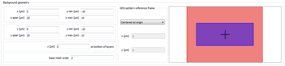
View the final structure in the CAD
The layer builder automatically sets up a structure group containing the objects. You can view and select the structures by expanding the layer builder in the Objects tree, as shown below. Note that the objects under the Layer builder cannot be edited directly: to make any changes you must edit the parent layer builder object.
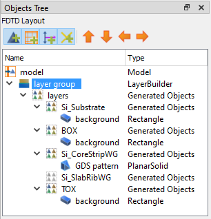
The Layer builder automatically sets the graphical rendering opacity of the structures it generates: background layers get alpha = 0.3 and grow layer get alpha = 0.8. Therefore, background layers are more transparent by default. However, the user can change the opacity of a layer using the script command setlayer, as explained in the next section.
Setting up from script
A layer builder can also be added and set up completely from script. The example script file layer_builder.lsf sets up the same structure described in Setting up from the GUI. As mentioned in Add and edit process layers, layers can be added one by one from scratch or all at once by loading a process file. The example shows how to do both by script.
The usage of the relevant script commands is summarized below. For more detailed information on each of them please visit their specific documentation:
- Add a layer builder object:
- addlayerbuilder: Adds a layer builder object to the simulation environment.
- Setup pattern geometry:
- Import/export GDS file:
- loadgdsfile: Loads a GDS file into a layer builder object.
- getcelllist and getlayerlist: Return the list of cells or layers associated with the loaded GDS.
- savegdsfile: Creates a GDS file with the pattern geometry from a layer builder object.
- Defining polygon vertices from script:
- set and get/getnamed: Define or access the polygon vertices stored in the layer builder object with “geometry” as property. See Format of polygon vertices data in Layer Builder for information on how the vertices are stored.
- Import/export GDS file:
- Add and edit process layers:
- From scratch:
- addlayer: Adds a process layer to the layer builder object.
- setlayer and getlayer: Set or retrieve the properties of the specified layer. In addition to the properties in the layer list in the GUI, you can also override the default graphical rendering opacity of the pattern and the background by using the properties “pattern alpha” or “background alpha”, respectively (see Viewing the final structure in the CAD).
- From/to a process file (.lbr):
- loadprocessfile: Loads the specified process file in a layer builder object.
- saveprocessfile: Exports the process information in a layer builder object as a process file.
- From scratch:
- Set up the background geometry:
Setting up active components
The procedure for setting up the Layer Builder for active components is similar to the one for passive components, apart from the additional steps for electrical/thermal material models and doping objects. Please refer to the Setting up from the GUI section for details of the steps common to passive and active components. In this section, we will show the typical flow for setting up active components using i) a process file containing layer definition for optical/thermal properties and doping and ii) a GDSII file containing geometry and doping pattern.
| NOTE: You need a Lumerical version 2022 R1.1 or later for a Layer Builder that supports doping objects as well as electrical, thermal, and index perturbation materials, enabling full active component design and simulation. |
1. Add a Layer Builder
2. Import the GDS file containing the doping pattern as well as the device geometry.
3. Define the process layers through the GUI or a script. Alternatively, you can import a pre-defined process file. For active components, the 'Doping' tab needs to be populated with details of each doping layer. This together with the doping region defined in the GDS file is used to automatically create matching doping objects in the Object Tree as shown below. Note that you need to add the CHARGE solver object, to make the doping objects visible.
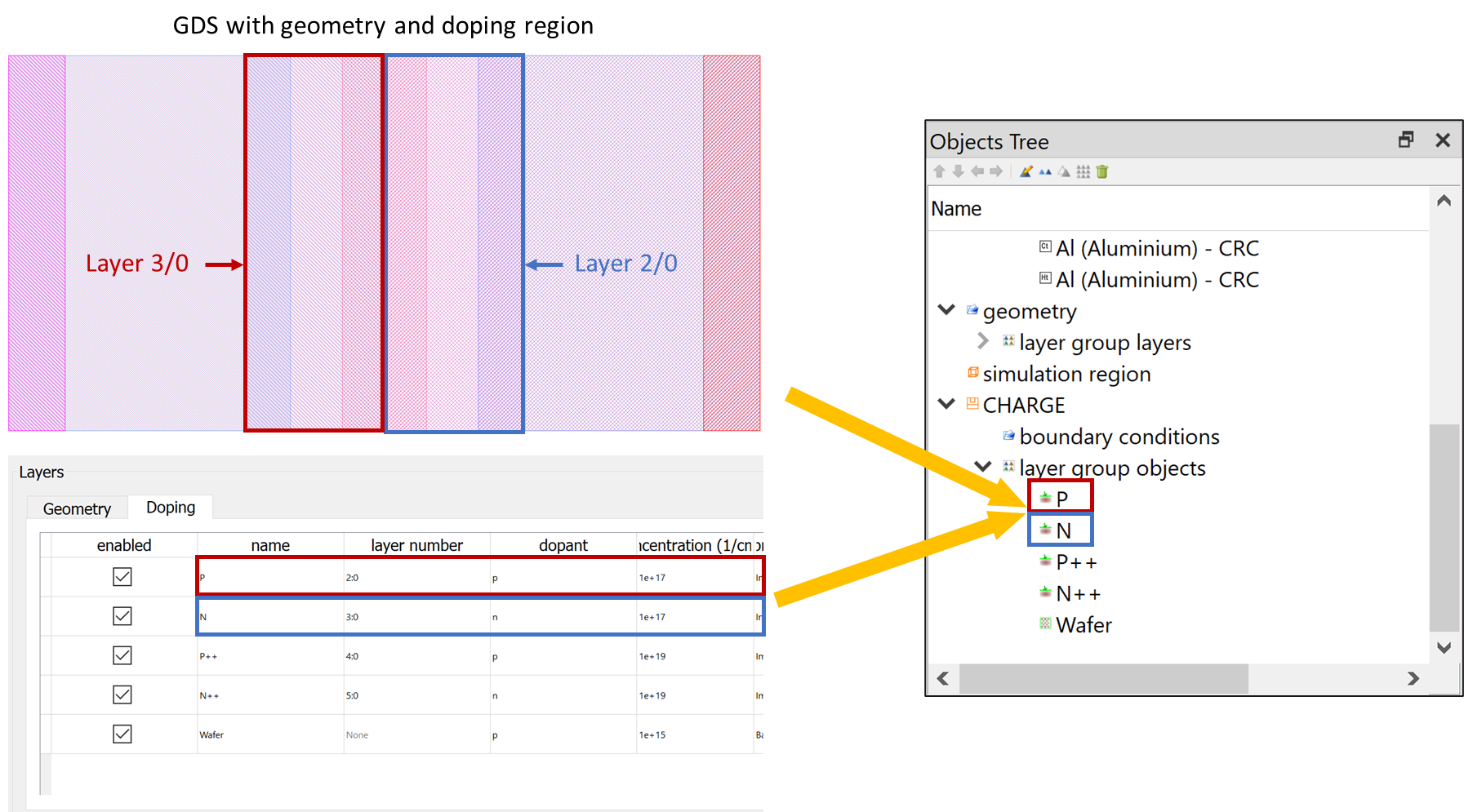
The Layer Builder allows Implant and Constant doping regions. The definitions of most of the parameters in the "Doping" tab can be found on the following pages:
Those parameters unique to the Layer Builder is as follows:
- layer number: The layer number of the GDS file containing the corresponding doping region.
- process: Specifies the type of doping region. Choose "Implant" and "Background". "Background" means a Constant doping region.
Example:
- Download the active.GDS and active.lbr.
- Add a Layer Builder and a CHARGE solver in DEVICE.
- Open the Layer Builder and import the GDS and process files into the Layer Builder.
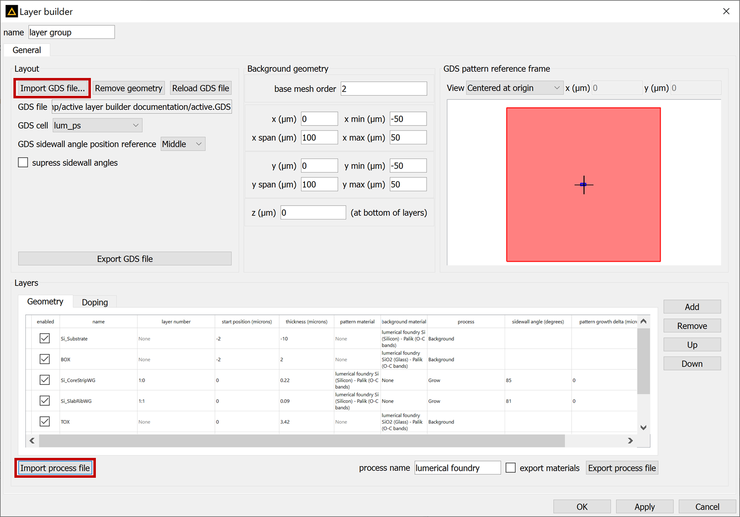
Once they are imported, the Object Tree is populated with auto-generated "layer group" objects and materials as below:
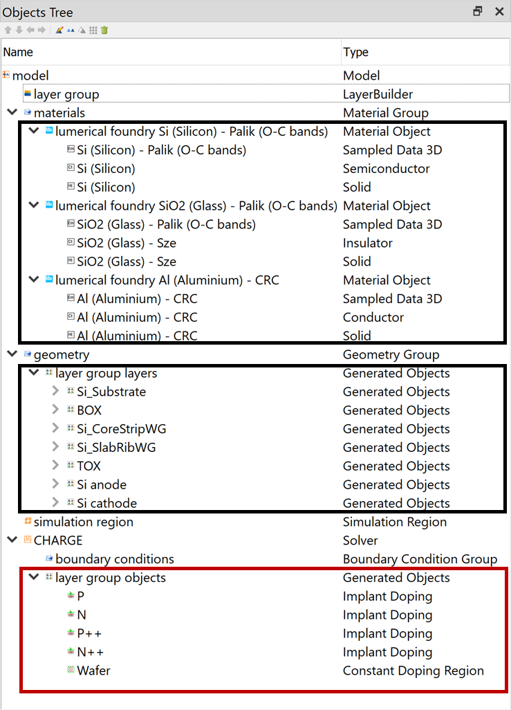
Appendix
Priority of overlapping process layers
The relative priority of structures generated by the Layer Builder when two or more structures overlap with each other is determined by these rules:
- Internally, the Layer Builder assigns mesh order as follows:
- All grow layers get the same mesh order, equal to base mesh order (see Set up the background geometry).
- All background layers get the same mesh order, equal to base mesh order + 2.
- As a consequence, grow layers always have higher priority than background layers regardless of their position in the layer list.
- Structures associated with each layer are generated in the same order as in the list of layers. Therefore, the priority between layers of the same process type is determined by the ordering in the list: layers at the bottom of the list will take priority over layers at the top of the tree.
Exporting and importing material data
As mentioned in Add and edit process layers, there are two different behaviors:
- When “export materials” is unchecked (default):
- Only the name of the materials used in the layer definitions is saved in the process file.
- When importing the process file in the Finite Difference IDE (FDTD and MODE), the Layer Builder will first create copies of the materials in the Material database that match the names provided in the process file. For the copied materials, the process name defined at the top of the Layer Builder Edit window is added to the original name. Therefore, the original materials in the database remain unchanged.
- When importing the process file in the Finite Element IDE (CHARGE, HEAT, DGTD and FEEM) the behavior is slightly different. In this case a new parent material, named according to the process name and the original material name in the process file, is created in the materials folder of the Objects Tree and all the optical/electrical/thermal properties are added based on the material names saved in the process file if they are found in the Optical/Electrical and Thermal Material databases. These properties of the parent material keep the original name in the Material database.
- Note that after the process file is imported, all the pattern and background material fields are automatically updated with the appropriate name of the copied materials.
- If the material saved in the process file does not exist in the Material database, the layers that use that material cannot be generated. This is one of the reasons why it is convenient to save the material data in the process file, as explained next.
- When "export materials" is checked:
- All the material properties including data and fitting settings are saved in the process file.
- When importing the process file, the Layer Builder will create new materials with the information contained in the process file. The process name defined at the top of the Layer Builder Edit window is added to the original name in the process file.
- This option is only available in the Finite Difference IDE (FDTD and MODE).
Format of polygon vertices data in Layer Builder
The polygon vertices of the patterns in a layer builder object can be loaded from a GDS file or by script. In either case, the vertices are saved as a struct with a field for each GDS layer (denoted with the layer number, including the data type):
- Each field of the struct is a cell array with as many elements as polygons in the GDS layer.
- Each element of the cell array is a N X 2 matrix where N is the number of vertices in the polygon. Each row is a pair of x and y coordinates.
Example
You can access the polygon vertices in the y-branch example using the following commands:
?vertices = getnamed("layer group","geometry");
Struct with fields:
10:0
1:0
68:0
69:0
?Si_layer = vertices.%1:0%;
Cell array with 17 elements
?size(Si_layer{1});
result:
16 2
You can edit any of the polygon vertices in the struct vertices and reload it in the layer builder object using:
select("layer group");
set("geometry", vertices);
You can also define the geometry completely from scratch as shown in the example below, where we define two circular patterns in the silicon layer:
# Define (x,y) coordinates of pattern for layer (example of a 2 circular patterns)
n_vertices = 100;
theta = linspace(0,2*pi,n_vertices+1);
theta = theta(1:(end-1)); #remove last point (duplicated, 0=2pi)
radius1 = 0.5e-6; xcent1 = 0; ycent1 = 0;
x1 = radius1*cos(theta)+xcent1; y1 = radius1*sin(theta)+ycent1; # circle 1
radius2 = 0.4e-6; xcent2 = 1e-6; ycent2 = 1e-6;
x2 = radius2*cos(theta)+xcent2; y2 = radius2*sin(theta)+ycent2; # circle 2

# Save vertices in structure with the format required by layer builder:
new_vertices = struct;
new_vertices.%1:0% = cell(2);
new_vertices.%1:0%{1} = [x1,y1];
new_vertices.%1:0%{2} = [x2,y2];

# Set geometry in Layer builder object
select("layer group");
set("geometry", new_vertices);
Process and optical material revision
When a process file is generated from a Layer Builder object (see Add and edit process layers), two revision hashes are automatically generated and saved in the process file: a process revision hash from the layer information in the layer list, and a material revision hash from the material properties if the checkbox “export materials” is enabled.
The revision hashes help detect changes in the process file after it has been generated (for example, if someone tampers with the process file by editing it in a text editor) or changes in the properties of materials from a process file after they have been imported. In either case, warning messages will be displayed under the Layer list specifying which of the two revisions failed:
- Process revision no longer matches reference from last imported file.
- Optical revision no longer matches reference from last imported file.
Dataset builder utility overview
FDTD MODE DGTD CHARGE HEAT FEEM

The dataset builder
![]()
button opens a wizard that enables the user to create an unstructured dataset and then (if appropriate) use the data to build structures and doping objects (in CHARGE only). It also generates a script file that can later be used to perform the same task using only the script environment. The dataset builder is powerful tool that facilitates the use of finite-element data imported into Lumerical's optical and electrical solvers.
Geometries and doping profiles can be created using 2D or 3D finite element data imported into the script workspace of FDTD, MODE, or CHARGE. The advantage of using the dataset builder is that the finite-element data can be imported from a variety of supported formats such as HDF5 (.h5), matlab data (.mat), tecplot (.dat), or Lumerical data file (.ldf), before being used to build unstructured datasets (and eventually complex structures and doping profiles).
The following example shows how the dataset builder can be used to create an unstructured dataset and build a structure along with its doping profile using data imported from an HDF5 file. The example is created in CHARGE. However, the work-flow will be identical in FDTD and MODE.
Unstructured dataset and finite-element data
The unstructured dataset is a useful format to store spatial data that is defined on a finite-element grid. A finite-element grid consists of triangles (in 2D) or tetrahedrons (in 3D), more commonly known as elements. The data is stored at the vertices of these elements and usually has a dimension of Nx1 (for unparameterized data), where N is the number of verteices. Three vertex matrices x, y, and z contains the x, y, and z coordinates of all the vertices, respectively, and have same the dimension of Nx1. Unlike rectilinear data where only the spatial data and the x, y, z coordinates are sufficient, in a finite-element grid, an additional matrix is needed to properly describe the spatial data, which is called the connectivity matrix. The connectivity matrix contains information about all the elements and stores the index of the vertices that create each of the elements. The dimension of the connectivity matrix is Mx3 (for 2D triangles) or Mx4 (for 3D tetrahedrons), where M is the number of elements in the finite-element grid. In the following figure, the different elements (triangles) and vertices of a (2D) finite-element space are shown along with the connectivity and vertex matrices.
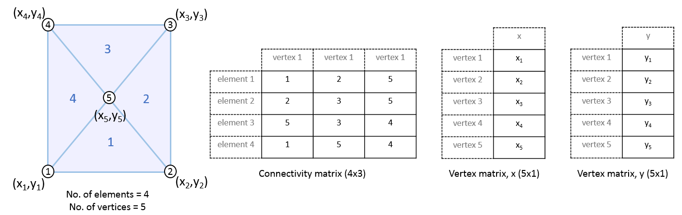
Apart from the fact that the unstructured dataset holds finite-element data, it behaves similar to the rectilinear datasets used in Lumerical's solvers. The dataset can be parameterized and it can have an arbitrary number of attributes (spatial data) and parameters. For details about the different datasets used in Lumerical's solvers, refer to the Datasets page.
Import finite element data into the workspace
The dataset builder works with the data available in the script workspace. Therefore, the data must be imported into the workspace before the dataset builder is used. In this example, we will import the finite element data from an HDF5 file. However, other file formats can also be used to import the necessary finite element data.
Download the "readh5file.lsf" script file and the "processdata.h5" HDF5 file. Open the script file in CHARGE and run it. The script will read the data and save the variables in the workspace. Note that the script prints the units for doping and dimension in the script prompt. For a detailed discussion on how to read HDF5 files, please refer to the knowledge base page related to reading HDF5 files.
readh5file;
Unit of doping is cm^-3
Unit of dimension is meter
Below is a screenshot of the script workspace after the data has been imported from the HDF5 file.
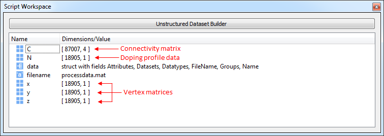
Build the unstructured dataset
Click on the build
![]()
button in the CHARGE interface and select the dataset builder
![]()
. This will open up the dataset builder wizard.
Select dimension
To get started, select the dimension of the finite element data. In this example, we will create a 3D structure, so select the 3D option.
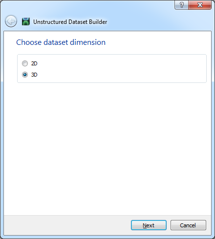
Select the connectivity matrix
Next select the connectivity matrix. The dataset builder wizard will automatically filter out the irrelevant matrices and will show only the matrices that have the proper values (integer) and dimension to be used as a connectivity matrix for 3D finite element data.
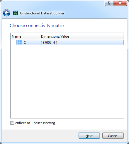
| Note: Sometimes the imported data may use a '0' based indexing. For such cases, enable the "enforce to 1-based indexing" option to make the data compatible with the 1-based indexing used by Lumerical's solvers. |
Select the vertex matrix / vertex table
The next step would be to select the vertex matrix or the vertex table containing the x, y, and z coordinates of the vertices. The wizard will again show only the matrices that have the proper dimension for the vertex matrix or the vertex table based on the selected connectivity matrix. The imported data in this example contains the x, y, z vertex matrices. They can be loaded on to the appropriate coordinates by using the arrow buttons. Once all the matrices are loaded, the wizard will show the x, y, z extent in the visualization window at the bottom.
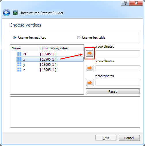
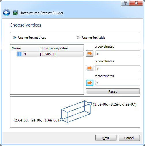
Once the vertex matrices are selected, the wizard will give the option to select the unit of the geometric data, change the orientation of the geometry by switching the coordinates, and mirror the geometry along any direction.
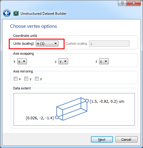
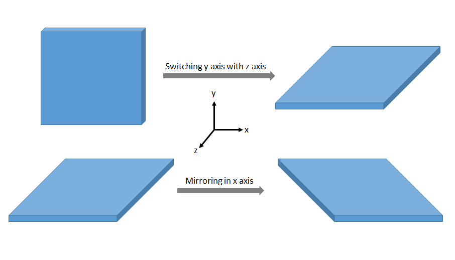
We will select the unit to be meter as our imported data is in meter (recall the information provided by the script). Note that for the "meter" selection, the scaling factor is 1e0 since in CHARGE (and also in the optical solvers), dimension is expressed in meter (SI unit). The user also has the option to select a custom scaling factor for their geometric data by selecting the custom scaling option from the drop down menu.
Once the unit has been selected, the visualization window will show the proper dimension of the geometry in micron which is the default dimension for length in the CAD environment.
| Note: Please note that the default unit for length in the CAD environment is micron. The user has the option to change this unit from the "Setting" tab. However, the dimension data saved by CHARGE and the unit for length that is used for all calculations in the script environment is in meter (SI unit). |
Choose parameters
Often, the values (attributes) in an unstructured dataset are saved as functions of some parameters such a bias voltage, temperature, etc. The next step in the dataset builder wizard is to select the parameters for the dataset being built. If no parameters are selected then the dataset builder assigns an empty parameter to the dataset for visualization purpose. Since the data in this example has no parameters, we select the "use default parameter" option. To learn more about parameters, check the Datasets page.
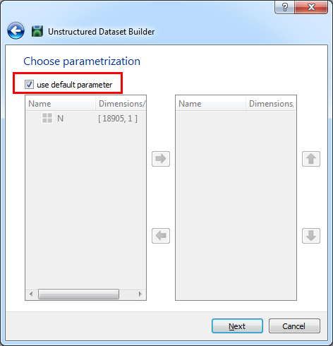
Choose attributes
The next step is to select the attributes. Based on the selection of the vertex matrix and the parameters, the dataset builder wizard will again filter the matrices in the script workspace and only the matrices that have the proper dimension will be viewed in the window. The user has the ability to select more than one attribute for a single unstructured dataset. In our imported HDF5 file, we have only one attribute which is the doping profile of the structure, N. We will select this matrix as our attribute in this step.
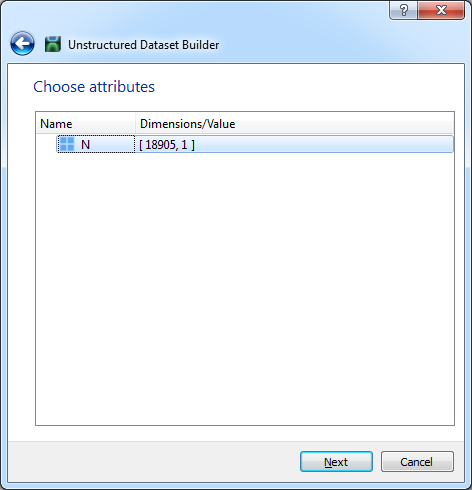
Save unstructured dataset
Finally, the unstructured dataset is ready to be created. To do this, simply choose a name for the dataset and click "Finish."
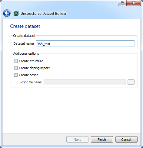
Visualize the unstructured dataset
Once the dataset is created, it can be viewed in the visualization window. To do this, right click on the dataset in the script workspace and click "Visualize."
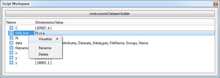
Build structures and doping objects
In the final page of the dataset builder wizard, there are options to create structures and doping profiles based on the unstructured dataset. To use this feature, enable the check boxes for "Create structure" and/or "Create doping import" (CHARGE only) and then click "Next."
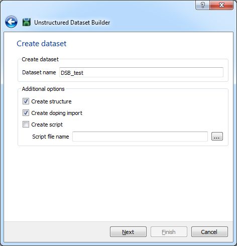
Create structure
If the "Create structure" option is enabled, the wizard moves to a new window where the structure can be named and a material can be assigned to it. For our structure, we choose the name "silicon" and the material "Si (Silicon)" from the drop down menu. Please note that the window also provides the option to override the default mesh order for the structure. In FDTD (and MODE), this window is different and has different fields to set the material properties appropriate for the corresponding solvers. A screenshot of the same window in FDTD is also shown below.
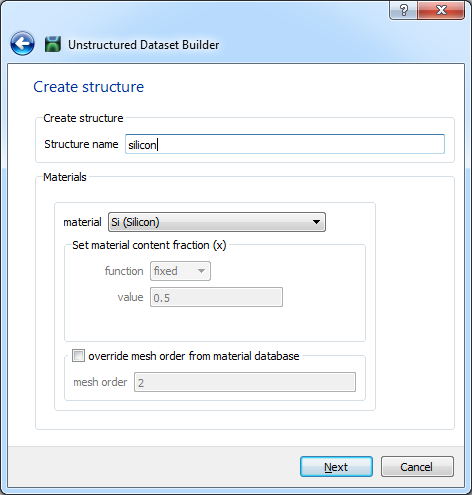
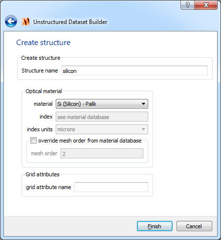
Create import doping (in CHARGE only)
If the "Create doping import" option is enabled, the wizard opens up a new window asking for the following inputs, i) the attributes that will be used to create the import doping objects, ii) the names of the import doping objects, iii) the units of doping in the used data, and iv) the doping types (n or p type). In this example, we have imported n-type doping values and the unit of the doping is cm^-3 (recall the information provided by the script). So we will choose the unit to be cm^-3 and the doping type to be "n." Please note that there is a scaling factor of 1e6 when we choose the unit to be cm^-3. This is because CHARGE uses a unit of m^-3 (SI unit) while creating the import doping objects.
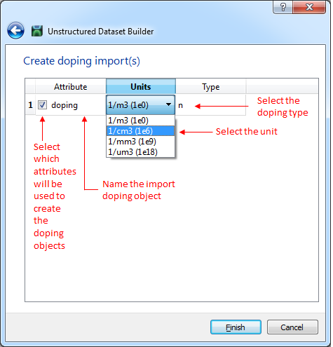
Generate script
The final window of the dataset builder also provides the option to create a script file that can perform the same tasks as the wizard using the choices made at different steps. This feature is very useful in automating the whole process of building datasets and creating structures and doping objects when generating complex structures from a large number of imported data. The script file script_out.lsf was created using the dataset builder and it can be used to perform all the tasks described in the preceding steps.
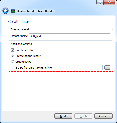
Test the created structure and doping profile
In order to check whether the structure has been created properly and the doping has been applied to the structure accurately, we can add a simulation region to the CAD environment to encompass the structure. In order to ensure that the entire simulation region has a material in it, we can create a background oxide that covers both the structure and the Device region. We will use the mesh override option to ensure that the oxide only fills the empty spaces and do not occupy the space where the (silicon) structure is present. Once the oxide and the Device region are in place, calculate the mesh only and right click on Device region to visualize the grid. The doping (N) plot will show whether the doping has been applied to the structure accurately.
In the attached "DSB_test.ldev" file, the background oxide and Device region has already been created. In order to see the resulting structure and doping, download and open the file along with the script_out.lsf script file. Open the CHARGE file and run the script. Once all the structures are generated, calculate the mesh, and visualize the grid from the Device region
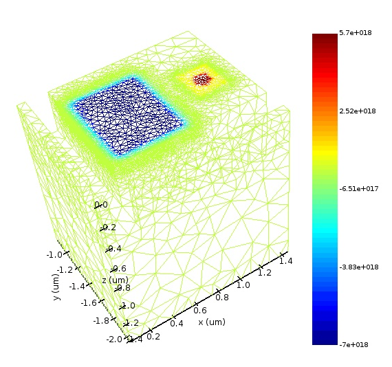
Always extend structures through PML boundary conditions
PML boundary conditions are designed to absorb all incident light. For best performance, physical structures should extend completely through the PML boundary condition region. The default settings in FDTD will automatically extend any structures which lie on the PML boundary through the PML. In some cases, such as for photonic crystals, it is better to disable this feature and draw the structures in the PML manually.
Simulation areas
A typical simulation is shown in the above screenshot. The simulation region outline is shown graphically in orange. When the boundary conditions are set to PML, the simulation region outline has some thickness. This creates three areas, labelled A, B, C in the above figure.
A - Simulation area of interest
This is the region that the user is interested in simulating. All important structures, sources and monitors should be defined in this area. The size of this area is set with the X,Y,Z span property of the simulation region. Monitors only collect data in this area. Monitors and sources larger than this area will be automatically truncated at the boundary.
B - Boundary condition area
Boundary conditions are applied in this region. For most types of boundary conditions (periodic, bloch, metal), this area is very thin (1 mesh cell thick). These boundary conditions do not need a large area to function. PML boundaries are different in that they require a larger area to properly absorb the fields. The size of this area is proportional to the number of PML layers used in the simulation, and inversely proportional to the mesh size.
C - Completely outside the simulation region
Everything in this area will be ignored because it is completely outside of the simulation region. It is ok to create objects in this area, but they will not be included in the simulation. This applies to structures, sources, and monitors.
Extending objects through the boundary condition area
During a simulation, the electromagnetic fields are calculated both within the simulation area (A) and within the boundary condition area (B). Since the fields are still being propagated in (B), it is important that the material properties are also defined here. An interface in this area will act like any other interface and cause reflections. All structures should extend completely through the boundary condition area to minimize these reflections. This is especially important when using many layers of PML. As more layers of PML are added, the boundary condition area will become larger.
The boundary conditions tab of the FDTD region, shown below, contains an option to extend structures through the PML. By default this option is selected.
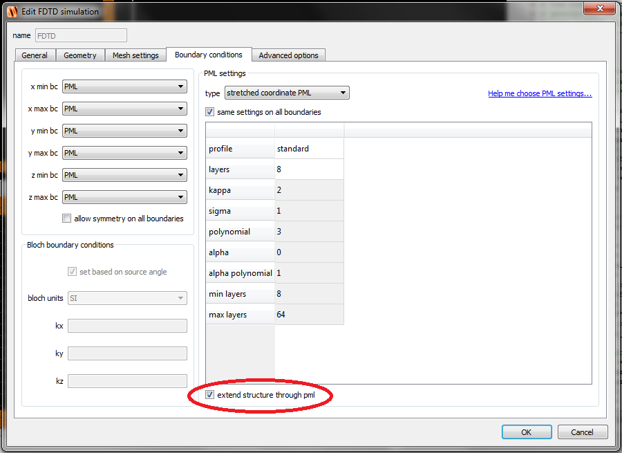
If the extend structure through PML option is selected, it will extend any structures that touch the inner PML boundary in the direction normal to the boundary. For instance, if the FDTD simulation contains the structure shown in the left image below, then the extend structure through PML option will create extend the structure as depicted on the right. This may not be ideal for all structures. In that case, you can uncheck this option and draw the structure through the PML.
Examples
The left figure below shows the correct setup when using substrates and other layers with PML. The layers should extend through the PML in both the X and Y directions. The right figure shows the layers terminated at the inside boundary of the PML. This interface may create an undesired reflection.
If the extend structures through PML option is selected, FDTD will automatically extend the structure in the right figure so that it gives the same results as the left figure.
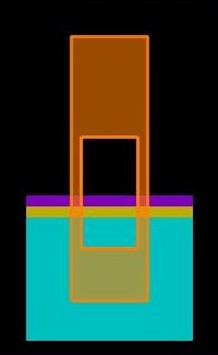
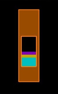
The left figure below shows the correct setup when using periodic structures with PML. The structures should extend through the PML boundary. The right figure shows the periodic structure only defined within the simulation volume. This effectively creates an impedance mis-match between the PC region and the boundary condition region. The mis-match will reduce the performance of the PML.
| Important: FDTD/MODE only meshs the structure as it is drawn on the left if the extend structures through PML checkbox is unchecked. Otherwise, the material which touches the inside PML boundary will be extended straight through the PML. When the 'extend' option is enabled, the structure will be meshed as drawn on the right, since none of the circles touch the inner edge of the PML boundaries. |
| Note: Sources and monitors will be automatically truncated to the inner simulation region. We recommend defining the sources and monitors to be larger than the simulation region. That way, if you need to make the simulation region larger, you don't need to re-size all the sources and monitors. |
| Note: Anything completely outside of the orange simulation boundary region has no effect on the simulation. In the photonic crystal example above, the two outermost rings of PC are not necessary. It is the third ring, within the PML boundary region, that is important to minimize reflections. |
Groups
Structure Groups - Simulation object
FDTD MODE DGTD CHARGE HEAT FEEM
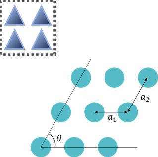
The structure group shown below and located in the associated file can be is used in the 2D square and triangular photonic crystal bandstructure calculation examples.
Elements of the structure group
A structure group consists of two elements
- a group of structure primitives
- a setup script to setup or edit the grouped primitives
The figure above shows the 2D photonic crystal array structure group from the attached triangular_lattice.fsp file. The structure group consists of an array of rods, whose radius, number, and spacing is set by the setup script.
Structure groups are created using the ADD STRUCTURE GROUP
![]()
option of the Groups button in the main toolbar. If you choose to edit a structure group object, then you will see that there are three tabs in the edit dialog box. The PROPERTIES tab contains input parameters for the script. In the PC structure group, the input parameters are the radius of the rods, the size of the array, the lattice spacing along the two axes of symmetry, and the angle between the axes. The SCRIPT tab contains the setup script that creates a physical structure. In the PC structure group, the script sets up the array of rods. The ROTATIONS tab is used to set the overall orientation of the group. The first two tabs will be discussed in more detail below.
Properties tab
The PROPERTIES tab is only available for structure groups, shown in the screenshot below. It contains all the input parameters that are needed to set up the physical structure. Custom user property variables may be added with the ADD button and removed with the REMOVE button.
There are two sections in the properties tab:
- ORIGIN: The location of the origin of the group, in the global coordinate frame.
- USER PROPERTIES: User properties are parameters that can be used to set up the structure. Each user property has a name and a type (number, frequency, etc). The user properties can be set manually in the edit GUI or through script commands.
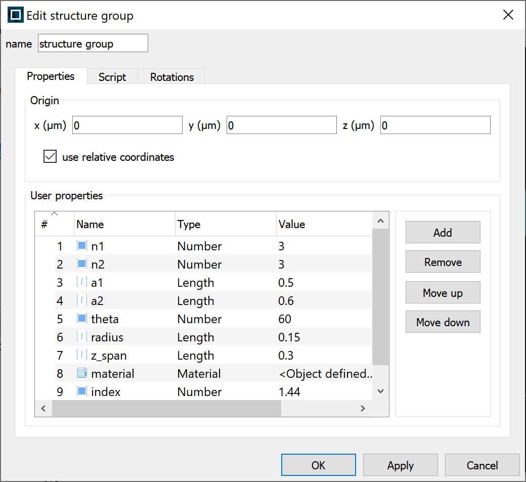
Script Tab
The SCRIPT tab, shown in the screenshot below, contains the setup script that is used to create and/or edit structures within the group. The script tab can contain script commands that are used to set up a structure or edit the properties of structures located within the structure group. The structure group has access to the user variables defined in the PROPERTIES tab and can change the properties of any objects that are contained in the group. The script does not have access to objects which are not located in the group and does not share the same variable space as the script prompt.
The following buttons and regions are available in the Script tab:
- SCRIPT: This is where the script commands are written. To find a list of script commands, see the Scripting Language section of the Reference Guide.
- TEST/SCRIPT OUTPUT: Press the TEST button to run the script. If there are no syntax errors in the script the SCRIPT OUTPUT will read <script complete>.
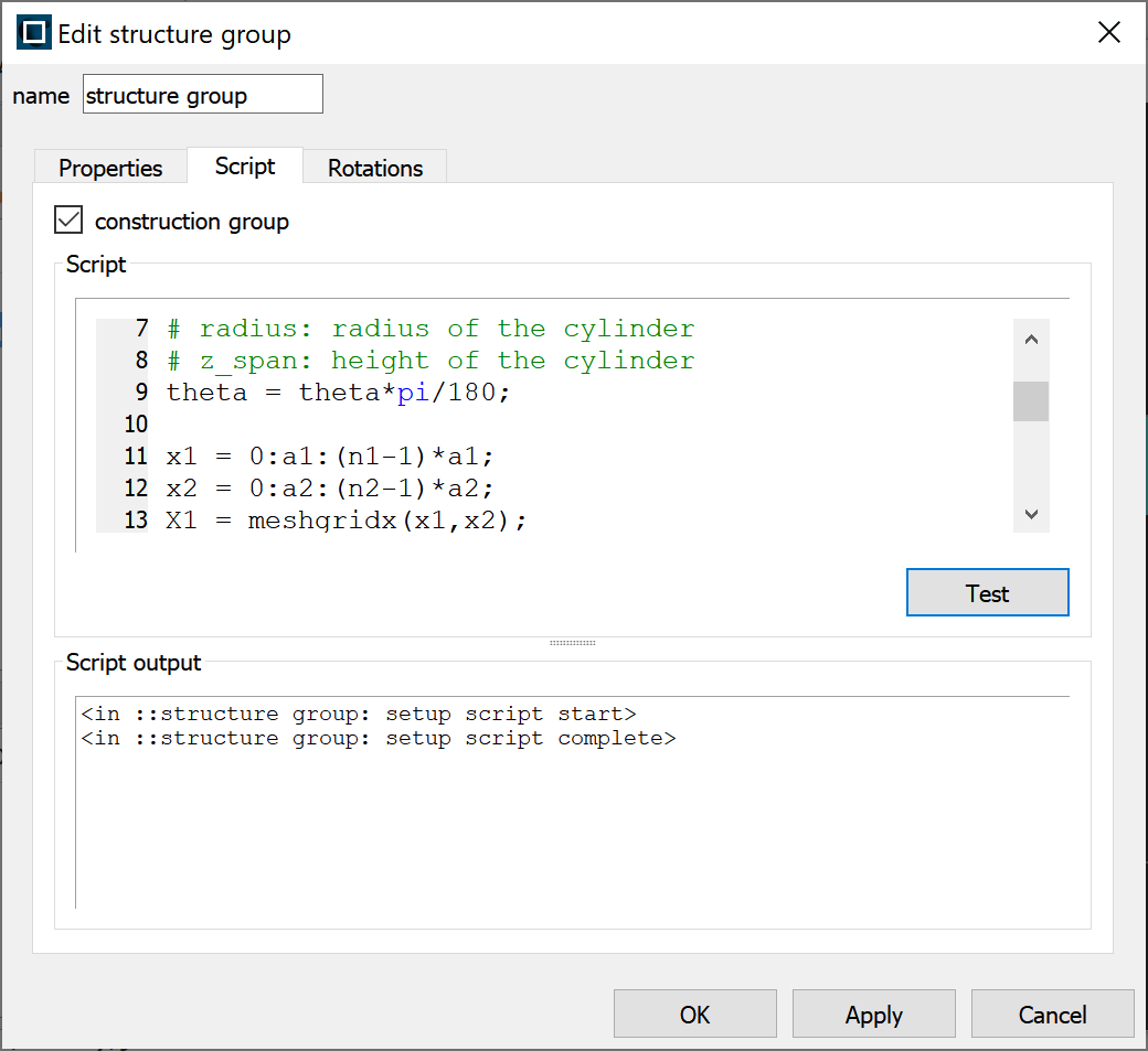
Note that:
- the user parameters are used in the script to create the array. For example, the user property "radius", which is highlighted in blue in the screenshot of the PROPERTIES tab is used in the following manner to set the radius of the rods to 120 nm.
addcircle;
set("radius",radius);
- the select and unselect script commands are used in the script. When these are called, only elements in the group are selected. The scope of the setup script is limited to objects within the group.
- the setup script does not have access to the global workspace variables (those defined in the script prompt or in a script file). The script has its own private variable workspace. In addition, any variables defined in the setup script cannot be obtained from the script prompt or from a script file.
- objects are created relative to the origin of the group. So for example, if the origin was set to (5,0,0) microns in the VARIABLES tab, then the following commands would add a rectangular structure centered at (10,0,0) microns, as measured in the global coordinate frame.
addrect;
set("x",5e-6);
- the TEST button runs the script and generates the array shown in the image at the top of this page. If there are no syntax errors in the script, you will see the line <script complete> in the script output. If there is a syntax error, the location of the error will be given in the script output. An example of an error message is: syntax error: prompt line: 38.
- the script is also run every time the TEST or OK button is pressed or a property of the structure group is changed with a script command.
Benefits of using structure groups
Parameter Sweeps:
Structure groups simplify parameter sweeps. The following lines can be used in a script file or script prompt to loop through one of the lattice parameters of the 2D photonic crystal array. Each time the set script command is called the setup script runs is executed, editing the array so that it has a the new lattice parameter. Also, these values can be used as parameter sweep variables or part of the figure of merit in optimizations.
a(i) = linspace(1e-6,6e-6,4) #array of lattice parameters
for(i=1:length(a)) {
switchtolayout;

#edit structure group
select("2D photonic crystal array");
set("ax",a(i));
run;

#run simulation

# do something

}
Copying and Pasting (Modularity):
Structure groups can be copied and pasted from one simulation to another using the CTRL+C and CTRL+V shortcut key combinations on the keyboard.
Simplifies running script files:
Master scripts can be kept shorter by moving some of the script within the group. This can be seen, for example, in the parameter sweep example. Also, in the script in the analysis groups, there is no risk of unintentionally overwriting variables. Any variables defined in a script file or in the script prompt become workspace variables and can be used or overwritten by any script that is run afterward. In contrast, the variables in the script of a structure group are not workspace variables, and the structure group script does not have access to the workspace variables
Creating a structure group from a script
It is possible to create a structure group from a script, as shown in the following example code:
addstructuregroup;
set("name","cube");
adduserprop("length",2,1e-6);
set("construction group",1);

# define the setup script by setting the 'script' property.
# Note that the entire script must be contained within a set of
# quote characters. Typically single quote characters are used
# to contain the entire string, which allows double quotes to be
# used within the script.

set('script','
addrect;
set("x span",length);
set("y span",length);
set("z span",length);

');
Analysis Groups - Simulation object
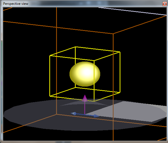
Analysis objects allow you to group monitors (similar to structure groups) and to analyze that monitor data. For example, a set of monitors can be grouped together to form a closed box. From the raw monitor data, the group can calculate quantities like cross sections and far field projections.
The files in this section were created using FDTD, but the same set up can be created using MODE Solution's propagator. Lumerical provides many built in analysis groups in our object library. Please press this button
![]()
to open the online library of analysis groups, or see object library for more details.
Analysis groups are container objects that can contain any simulation object and associated script functions which can be used to customize data analysis. For example, an absorption monitor group can be created with a power monitor, an index monitor, and the script function that calculates absorption from these objects. One can also automate an optimization/parameter sweep procedure using an analysis group made of structures/simulation regions/sources/monitors, and use the script function to update each parameter accordingly.
Analysis groups are created using the ADD ANALYSIS GROUP
![]()
button in the layout editor. If you choose to edit an analysis object, then you will see that there are two tabs in the edit dialog box
- the SETUP TAB contains all the information about the monitors
- the ANALYSIS TAB contains the analysis routine and input and output parameters to the analysis routine.
The figure above shows this example simulation file. The box of monitors will be used to measure the power absorbed in the particle.
Using Analysis Groups
Some important script functions which can be used in script files or the script prompt are:
set("object","parameter",value);         # to set the values of the group parameters
runanalysis;   # to run the analysis routines
getdata();     # to obtain raw matrix data from the monitors.
Once an analysis routine has been run, any variables that were defined in the analysis script AND included in the results section of the VARIABLES tab can be obtained using the following commands:
getresults; # get packaged dataset
Datasets are a way to package the result data (such as transmitted power) together with any associated information (such as the frequency vector).
Example:
Begin by opening and running the associated simulation, usr_transmission_box.fsp. Select the analysis group. Then enter the following script commands in the script prompt. The commands disable the option for the analysis object to create its own plots, runs the analysis routine, gets the results, finally sends them to the visualizer.
setnamed("trans_box","plot results",0);
runanalysis;
Pabs = getresult("trans_box","T");
?Pabs;
?Pabs.T;
?Pabs.f;
visualize(Pabs);
There is one result from this object: the power transmission out of the box (T) as a function of frequency.
You can also access the analysis object results through the graphical interface, as shown below:
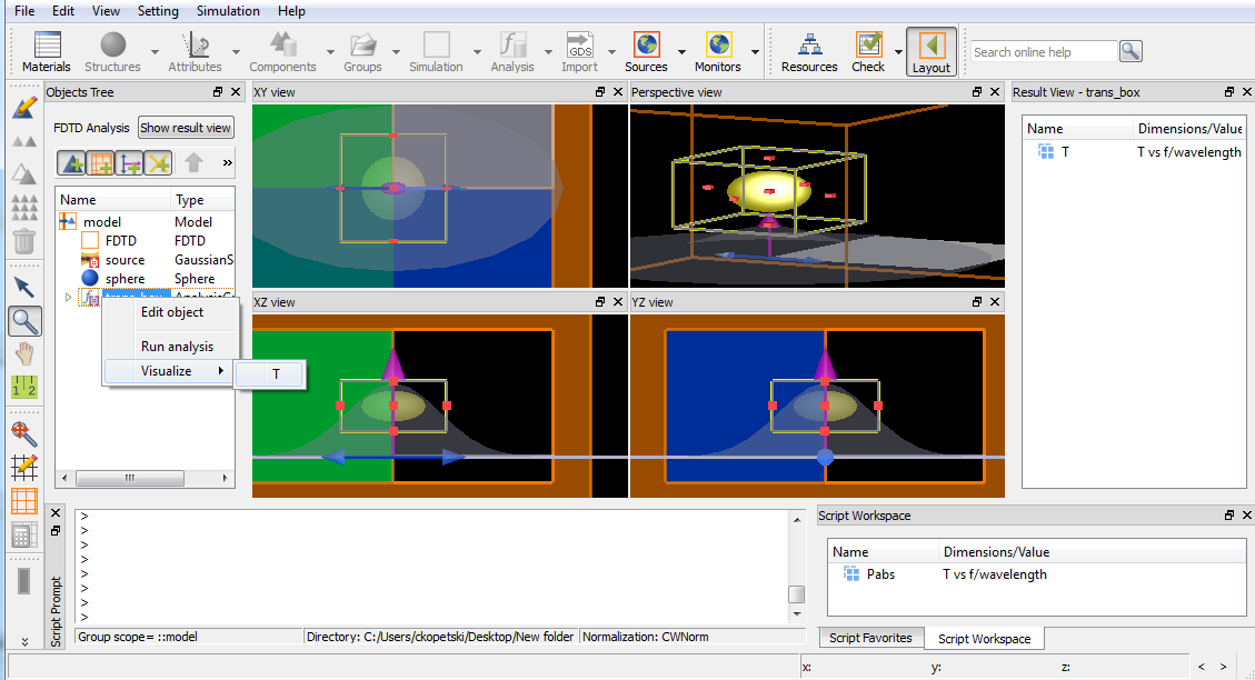
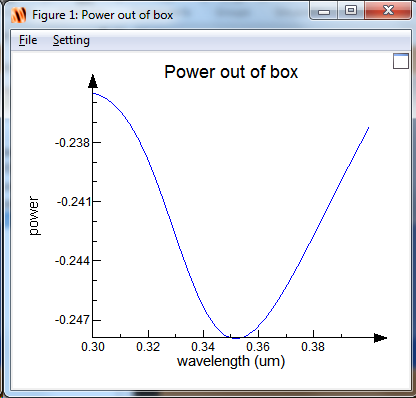
Setup - Variables
The Setup - VARIABLES tab contains user properties, which are input parameters for the script that is located in the SCRIPT tab. The screenshot above shows the VARIABLES tab for the scattering box analysis group in the usr_transmission_box.fsp file. The scattering box consists of a rectangular box of power monitors. The widths of the monitors are given by the user properties x span, y span, and z span.
Setup - Script
Script commands are written in the Setup - SCRIPT tab. To find a list of script commands, see the Scripting Language.
Note that:
- the setup script can only be used to add, delete, edit or get the properties of objects in the group. For example, the command selectall; selects all of the monitors located inside of the group, while ignoring those outside.
- objects are created relative to the origin of the group. For example, if the origin was set to (5,0,0) microns in the variables tab, then the following commands would add a power monitor centered at (10,0,0) microns.
addpower; set("x",5e-6);
- the script uses the input parameters to set up the structure (the % operator allows you to use variables with spaces in their name)
set("x span",%x span%);
- the setup script does not have access to workspace variables (those defined in the script prompt or in a script file). In addition, any variables defined in the setup script cannot be obtained from the script prompt or from a script file.
- the script can be debugged by pressing the TEST button. If there are no syntax errors or break commands in the script, you will see the line <script complete> in the script output. If there is a syntax error, the location of the error will be given in the script output. An example of an error message is: syntax error: prompt line: 38.
- the script is also run every time the OK button is pressed or a property of the analysis group is changed from the command line
- it is only possible to edit information in the SETUP tab in layout mode, the edited information will not be saved.
- usage of the "construction group" option means that objects are added from the script and changes to child objects will not be saved.
Analysis - Variables
The Analysis - VARIABLES tab contains all input parameters in the top half, and the output parameters (named results) in the bottom half. Parameters can be added and removed using the respective buttons. The screenshot above depicts the VARIABLES tab for the scattering box analysis group in the usr_transmission_box.fsp file. The VARIABLES tab contains two sets of variables and two buttons.
- PARAMETERS: This section contains all the input parameters
- RESULTS: The results section includes all the output parameters of the script. Once the analysis script that has been run, only the parameters that are both defined in the results section and initialized in the analysis script can be obtained from outside the analysis object.
- SAVE ANALYSIS button: Saves any changes made in the analysis tab (only in analysis mode)
- RUN ANALYSIS button: Runs the analysis script (only in analysis mode)
Analysis - Script
The Analysis - SCRIPT tab contains a customized analysis routine. The script has access to the input parameters defined in the VARIABLES tab, and can get data from any of the monitors located in the group. However, it cannot get data from monitors or sources not located inside that group. Scripts in analysis groups do not use the global variable space from the script prompt and script file editor. The results from the script can be obtained in the script prompt by setting up output parameters in the variables tab.
The following buttons and regions are available in the SCRIPT tab:
- ANALYSIS SCRIPT: This is where the script commands are written. To find a list of script commands, see the Scripting Language section of the Reference Guide.
- ANALYSIS SCRIPT OUTPUT: Press the RUN ANALYSIS button to run the script. If there are no syntax errors in the script the SCRIPT OUTPUT will read <script complete>. In addition, the analysis script output will contain any results from the "?" script command.
- RUN ANALYSIS: Pressing the run analysis prompt runs the analysis script and saves the results. This button can only be pressed when the simulation is in analysis mode.
- SAVE ANALYSIS: Pressing this button saves changes made to the analysis script (even when in analysis mode).
The SCRIPT tab of an analysis object is shown below. The note highlighted in yellow at the top of the dialog window says it is now in analysis mode.
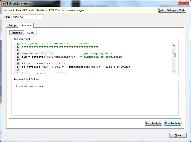
Note that,
- entries in the ANALYSIS tab can be edited in both the layout and the analysis modes. In layout mode, there are two buttons in the lower right hand corner of the screen: OK and CANCEL. In analysis mode, any changes to the variables can be saved using the SAVE ANALYSIS button at the bottom of the tab. The RUN ANALYSIS button runs the analysis script located in the SCRIPT tab.
- once an analysis routine has run, the results (output parameters) become monitor data, which can be accessed from the script prompt or a script file in the same manner that monitor data is accessed for simple monitors. However, the analysis script can only obtain monitor data from the monitors in the group. It is not possible to select the monitors and get their properties or use variables defined in the setup tab.
- the analysis script does not have access to workspace variables (those defined in the script prompt or in a script file). In addition, any variables defined in the analysis script cannot be obtained from the script prompt or from a script file.
- if the RUN ANALYSIS button is pressed, the ANALYSIS SCRIPT OUTPUT will contain the results of the analysis script. Once the script has run to completion, if there are no syntax errors or break commands in the script, you will see the line <script complete> in the script output. If there is a syntax error, the location of the error will be given in the script output. An example of an error message is: syntax error: prompt line: 38.
- the analysis script makes use of the parameters, for example
if(%make plots%){...}
- the results variables are defined in the script, for example
f=getdata("x2","f"); # get frequency data
- print variables or comments to the analysis script output by prefacing the lines with the ? operator, the value computed for the output parameter is printed in the Analysis Script Output portion of the window. If you run the analysis from the script prompt or a script file, these lines are not printed to the script prompt. For example, the first comment in the analysis script output comes from the following line in the analysis code:
?"Projecting in x-y plane";
- if you need to stop a script while it is running, press the ESC key on the keyboard. This will stop the analysis script from running, and close the edit dialog window.
Results
Various custom results are returned by the analysis group objects.
Components - Simulation object
The
![]()
button opens the structure section of the Object library. Components are more parameterized complex structures built from one or several primitives. These objects enable users to quickly setup common (but often difficult to construct) structures. See the in-product library for a full list of objects. Examples include:
Tips for creating structures with rounded corners
Tips for creating waveguide bends using the path object
Tips for creating spiral and helix geometries
Analysis - Simulation object
The
![]()
button includes options to open the Analysis section of the Object library. The library contains additional analysis objects that can be used in your simulation. See the in-product library for a full list of objects. Examples include:
Creating curved and angled monitors
Far field projections from a box of monitors
Changing the far field refractive index analysis object
Calculating charge distributions and currents in metals induced by an optical field
Attributes
np Density and Temperature Index Perturbation - Simulation object
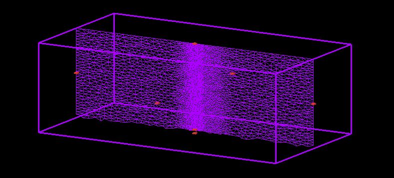
This page describes how to use the np Density and Temperature grid attribute objects to export electron-hole (np) density and temperature grid attribute recorded on a finite-element mesh directly from a CHARGE and HEAT simulation, and import it to FDTD or MODE.
Exporting index perturbation grid attributes from CHARGE and HEAT
np density grid attributeTo export np density data, the simulation file should contain an unstructured data set called ‘charge’ with scalar attributes ‘n’ and ‘p’. This would typically be exported from CHARGE as shown in the Mach Zehnder example. This can be done by right-clicking the charge monitor and selecting the save data with a user-specified filename. |
|
Temperature grid attributeThe temperature grid attribute data can be exported from HEAT using scripts. Once a simulation has run, click on the 'HEAT' solver object in the object tree. This will bring up the results related to the thermal analysis. The dataset called 'thermal' is the one to be export. The script as shown below can be used to do that: out = getresult("HEAT","thermal");
matlabsave("filename.mat",out); |
|
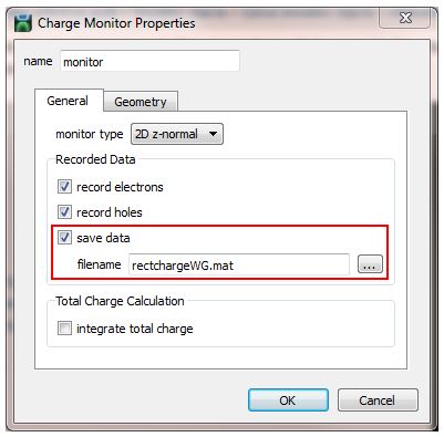
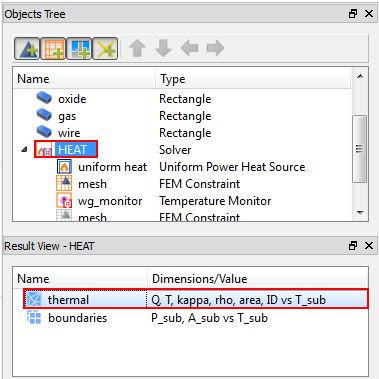
Importing index perturbation grid attributes to FDTD or MODE
The procedure for importing the np density and temperature grid attributes are the same.
Import using GUI
|
|
Import using scriptIt is also possible to import the np density and temperature grid attributes using scripts. Please refer to importdataset for further information. | |
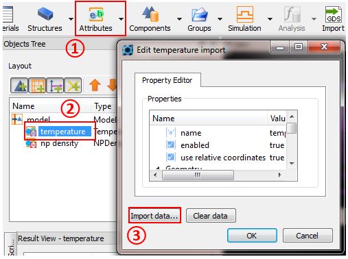
Creating an index perturbation material model
The np density and temperature attributes contain information about the charge density and temperature for the specified region in the simulation. The information needs to be translated into index changes by creating an index perturbation material model. Below are steps to be taken to create such material model.
| 1. Click 'Material' button from the main menu 2. Click 'Add' and select 'index perturbation' material model 3. Specify the material name 4. In the material properties, select the type(s) of index perturbation to be included in the material model, ie. np density and temperature. You can include only one of them or both. The index of the base material is then perturbed in accordance with options you choose for the conversion of np density / temperature to index changes. There are three conversion options available for np Density grid attribute:
and two options for Temperature grid attribute:
For more information about models for np Density material, please visit Charge to index conversion. |
|
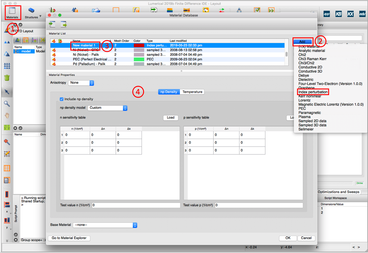
Note: Parameters for the models
These parameters are material and frequency dependent, the default parameters are set for silicon at 1.55 um.
Charge distribution to change in refractive index theory
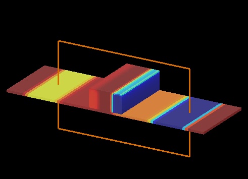
This section describes the models used to calculate perturbation in refractive index for optical simulations in MODE and FDTD based on imported charge density data from CHARGE simulations.
Theory behind the generalized Drude (Plasma) model
From the Plasma-Drude model ( Henry et al.), the overall refractive index, that is, the unperturbed index plus the change in the index can be calculated from overall carrier density as follows:
n+ik= ⎷εm−e2ω(nm∗eω+ie/μe+pm∗hω+ie/μh)ε0
where electrons and holes are treated as purely free carriers and n,p are the carrier densities, and εm is the permittivity of the unperturbed material, m∗e/h
is the effective mass of electrons/holes, and μe/h
is the mobility of electrons/holes. Note that in this model, the coefficients are frequency dependent. For cases where the electron and hole mobility values are large, the equation reduces to:
n+ik= ⎷εm−e2ω2(nm∗e+pm∗h)ε0
Theory behind the Drude expansion model
An expansion of the above Drude model at a particular wavelength assuming complex refractive indices can also be calculated from the change in carrier density for most semiconductors as follows:
Δn=−(e2λ28π2c2ε0n)[ΔNem∗ce+ΔNhm∗ch]
Δα=(e3λ24π2c3ε0n)[ΔNem∗ce2μe+ΔNhm∗ch2μh]
where,
e is the electronic change,
ε0 is the permittivity of free space,
n is the index of the unperturbed material,
m is the effective mass of holes/electrons and u is the electron/hole mobility.
m*ce/h is the conductivity effective mass of electrons/holes
μe/h is the electron/hole mobility.
ΔNe/h is the change in electron/hole carrier density.
Note that in this model, the coefficients are wavelength dependent.
Theory behind the silicon model
The above wavelength dependant model works for most semiconductors; however, there is another model to more accurately describe the effect of carrier density on refractive index in Silicon by Soref et al. In this model, the coefficients are different depending on the wavelength.
Δn=(dnAp)(ΔP)dnEp+(dnAn)(ΔN)dnEn
Δα=(dαAp)(ΔP)dαEp+(dαAn)(ΔN)dαEn
where,
Δn is the refractive index change
Δα is the absorption coefficient variation in cm-1
ΔP is the hole concentration change in cm-3
ΔN is the electron concentration change in cm-3
dαAp
is 6e-18 for 1.55 um
dαAn
is 8.5e-18 for 1.55 um
dnAp
is -8.5e-18 for 1.55 um
dnAn
is -8.8e-22 for 1.55 um
Note that in this model, the coefficients are wavelength dependent.
Theory behind the Custom model
For electro-optic devices, Δn and Δk due to carrier concentration variation (plasma effect, band filling effect and bandgap shrinkage) are sometimes measured or computed in separate files. For III-V materials, The Soref and Bennett model cannot describe their variations with high accuracy on a broad range of carrier concentration. The 'Custom' option provides users the option to load user data (Δn and Δk VS carrier concentration) from a text file. Linear interpolation are used to interpolate the user's data and MODE can then use these interpolated data (and the carrier concentration distributions from Charge) to compute the effective indexes.
In the Custom model, "n sensitivity table" and "p sensitivity table", take a matrix argument, similar to "temperature sensitivity table".
Structure group for conversion of carrier density to refractive index change
A .ldf file will contain the carrier density data calculated from CHARGE which will be imported into the structure. Depending on which product you use, FDTD or MODE, open the WgImport.fsp or WgImport.lms. The WgImport object has been created and defined in this file. Make sure you also download the ldf file(s). The same geometry as the one set up in the original CHARGE simulation has to be set up in MODE/FDTD, except that an import (n,k) object is used for the waveguide section. The structure group will take the carrier density information and calculate the corresponding changes in the real and imaginary parts of refractive index of the material according to one of the above formulations. In the CHARGE simulation, the voltage is swept and the corresponding carrier density change is calculated which in turn results in a change in the index. The .ldf file will include x_data, y_data, z_data, dn_data, dp_data and v.
The generalized Drude (Plasma) model
Right click on the ChargeToIndex_Drude objects in either the MODE or FDTD project files and click Edit. In the window that opens, under the properties tab, several variables can be defined by the user.
|
| V is the index of the voltage array over which the sweep in CHARGE was done. filename is set to the name of the .ldf file saved in the CHARGE script. lambda is the wavelength of interest (in um units). make_plots is set to 1 to generate plots of doping densities and the imported n,k values. mch,mce effective mass of holes/electrons ue, uh carrier mobility waveguide n/k are the nominal index and absorption coefficient values in silicon at wavelength lambda. |
Under the script tab of the ChargeToIndex_Drude, you will find the script that loads the .ldf file, uses the wavelength and the nominal n value to calculate the coefficients in the above equation and from that, calculates the real and imaginary parts of refractive index and creates an import (n,k) object with (n,k) values resulting from the bias value that corresponds to index V.
Click "test", to make sure the object is correctly created from the .ldf file.
The structure is now ready to be analyzed in either MODE or FDTD for further characterization. For an example of the full process from the calculation of charge in CHARGE to the calculation of index change in MODE using the Drude-plasma model please see the Metamaterial application example in the CHARGE knowledgebase.
The Drude expansion model
Right click on the WgImport_Drude objects in either the MODE or FDTD project files and click Edit. In the window that opens, under the properties tab, several variables can be defined by the user.
|
| V is the index of the voltage array over which the sweep in CHARGE was done. filename is set to the name of the .ldf file saved in the CHARGE script. lambda is the wavelength of interest (in um units). make_plots is set to 1 to generate plots of doping densities and the imported n,k values. mch,mce effective mass of holes/electrons ue,uh electron/hole mobility waveguide n/k are the nominal index and absorption coefficient values in silicon at wavelength lambda. |
Under the script tab of the WgImport_Drude object, you will find the script that loads the .ldf file, uses the wavelength to calculate the coefficients in the above equation and from that, calculates the change in refractive index and absorption coefficients and creates an import (n,k) object with (n,k) values resulting from the bias value that corresponds to index V.
Click "test", to make sure the object is correctly created from the .ldf file.
The structure is now ready to be analyzed in either MODE or FDTD for further characterization.
The Silicon model
Right click on the ChargeToIndex_Silicon objects in either the MODE or FDTD project files and click Edit. In the window that opens, under the properties tab, several variables can be defined by the user.
|
| V is the index of the voltage array over which the sweep in CHARGE was done. The coefficients for the equation to convert the change in carrier density to change in (n,k) are defined as follows (see reference 1); Δα=(dαAp)(ΔP)dαEp+(dαAn)(ΔN)dαEn |
Δn=(dnAp)(ΔP)dnEp+(dnAn)(ΔN)dnEn
| filename is set to the name of the .ldf file saved in the CHARGE script. lambda is the wavelength of interest (in um units). make_plots is set to 1 to generate plots of doping densities and the imported n,k values. waveguide n/k are the nominal index and absorption coefficient values in silicon at wavelength lambda. |
Under the script tab of the ChargeToIndex_Silicon object, you will find the script that loads the .ldf file, uses the aforementioned coefficients to calculate the change in refractive index and absorption coefficients and creates an import (n,k) object with (n,k) values resulting from the bias value that corresponds to index V.
Click "test", to make sure the object is correctly created from the .ldf file.
The structure is now ready to be analyzed in either MODE or FDTD for further characterization. For an example of the full process from the calculation of charge in CHARGE to the calculation of index change in MODE using the Silicon model please see the MZI getting started example.
References
- Henry, C. H.; Logan, R. A.; Bertness, K. A. Journal of Applied Physics, vol. 52, (1981), p. 4457-4461.
- R. A. Soref and B. R. Bennett, SPIE Integr. Opt. Circuit Eng. 704, 32 (1987).
Temperature dependent refractive index models

This section describes the models used to calculate perturbation in refractive index for optical simulations in MODE and FDTD based on imported temperature profile data from HEAT simulations.
Linear sensitivity model
The simpler model used to calculate index perturbation due to temperature variation assumes a linear dependency. The complex refractive index of a material at temperature T is given by,
n+ik=(nref+Δn)+i(kref+Δk)
where, n is the real and k is the imaginary part of the refractive index at temperature T, nref is the real and kref is the imaginary part of the unperturbed refractive index at temperature Tref, and Δn is the change in the real part and Δk is the change in the imaginary part of the refractive index. The values of Δn and Δk are given by,
Δn=dndT(T−Tref)
Δk=dkdT(T−Tref)
where, dn/dT and dk/dT are the rate of change in the real and imaginary part of refractive index, respectively. In the linear sensitivity model, the rate of change in refractive index is assumed to be constant at reference temperature Tref and is used as a material property in the "index perturbation" type material.
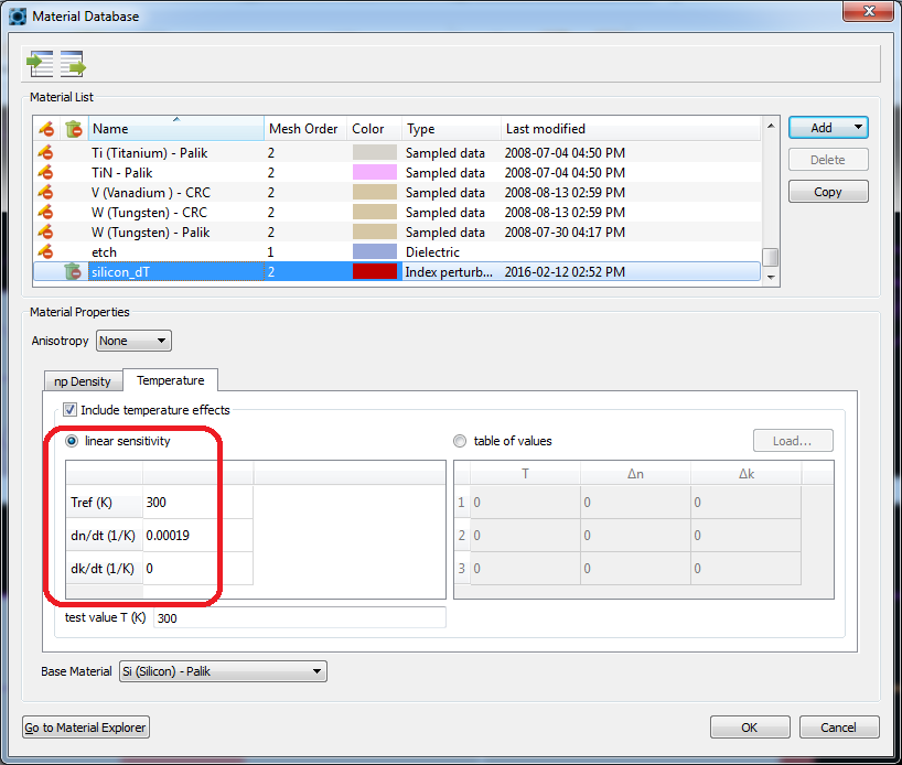
Nonlinear (tabular) model
The second model available for modeling index perturbation due to temperature variation allows for the modeling of nonlinear sensitivity. The nonlinear variation of refractive index can be given as an input in tabular form to the "index perturbation" type material. The effective index of the material at temperature T is then given by,
n+ik=(nref+Δn)+i(kref+Δk)
where, n is the real and k is the imaginary part of the refractive index at temperature T, nref is the real and kref is the imaginary part of the unperturbed refractive index at temperature Tref (300 K for the materials in the default material database), and Δn is the change in the real part and Δk is the change in the imaginary part of the refractive index. For a nonlinear temperature sensitivity, Δn and Δk are functions of temperature T.
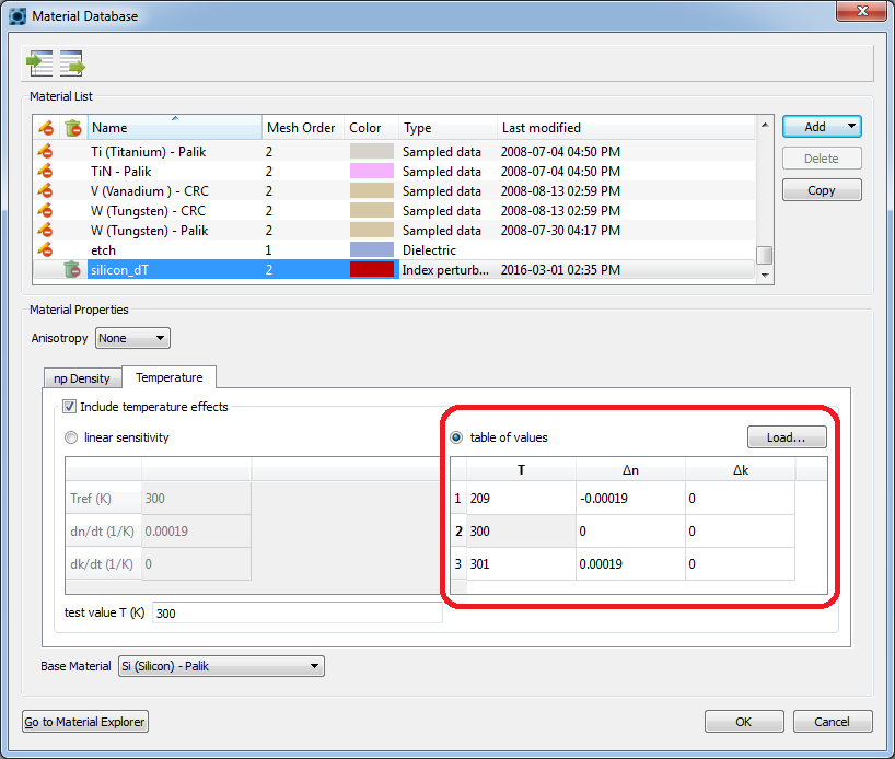
| NOTE: At T = Tref, the values of Δn and Δk should be zero. |
Simulation
Simulation objects are used to define simulation parameters like boundary conditions and mesh size. More information about the solver algorithms can be found in the Solvers section.
FDTD solver - Simulation Object
![]()
General tab
- DIMENSION: The dimension of the simulation region (2D or 3D).
- BACKGROUND INDEX: The refractive index of the surrounding, background medium in the simulation region.
- SIMULATION TIME: The maximum duration of the simulation to be performed. The actual simulation may be shorter if the autoshutoff criteria are satisfied before this maximum simulation time is exceeded.
- SIMULATION TEMPERATURE (K): The simulation temperature, for simulations that include temperature dependent objects.
Geometry tab
- X, Y, Z: The center position of the simulation region
- X MIN, X MAX: X min, X max position
- Y MIN, Y MAX: Y min, Y max position
- Z MIN, Z MAX: Z min, Z max position
- X SPAN, Y SPAN, Z SPAN: X, Y, Z span of the simulation region
Mesh settings tab
Mesh type
Three types of mesh generation algorithms are available, as described below
- Auto non-uniform (default):
A non-uniform mesh is automatically generated based on the mesh accuracy slider bar. It is strongly recommended to start with a mesh accuracy of 1-2 for initial simulations to make the simulations run quickly. Higher mesh accuracies can be used for convergence testing if necessary.
The MESH ACCURACY parameter is an integer from 1-8, where 1 is low accuracy, and 8 is high accuracy (smaller mesh). Many factors go into the meshing algorithm, including source wavelength, material properties and the structure geometry. The number of mesh points per wavelength (ppw) is a major considerations for the meshing algorithm. Accuracy 1 corresponds to a target of 6 ppw. Acc 2 ->10 ppw, Acc 3 ->14ppw, and so on, in increments of 4 ppw per point on the slider bar. It is important to remember that wavelength is inversely proportional to the refractive index. In high index materials, the effective wavelength is smaller, meaning that the meshing algorithm will use a smaller mesh in high index materials.
- Custom non-uniform:
This setting allows the user to additional options to customize how the non-uniform mesh is generated. If setting the mesh cells using wavelength, the default setting of 10 is sufficient in general, but may be reduced to 6-8 for coarse simulations.
The grading factor determines the maximum rate at which the mesh can be modified. For example, if dx(i+1) = a*dx(i), then 1/(GRADING FACTOR) <= a <= GRADING FACTOR. The grading factor should be between 1 and 2. The default setting is sqrt(2).
- Uniform:
A uniform mesh is applied to the entire simulation volume, regardless of any material properties. If a mesh override region is used in conjunction with this option, the override region will force the mesh size everywhere, not just within the override region (afterall, the mesh is uniform).
Mesh Refinement
Mesh Refinement: Mesh refinement can give sub-cell accuracy for a simulation. See the Mesh refinement options page for more information.
Time Step:
- DT STABILITY FACTOR: A setting which determines the size of the time step used during the simulation, defined as a fraction of the Courant numerical stability limit. A larger number will result in faster simulation times, and a smaller number will result in slower simulation times. The Courant stability condition requires that this setting must be less than 1 for the FDTD algorithm to remain numerically stable.
- DT: The time step of the FDTD/Propagator simulation. This is determined by the values of the spatial grid to ensure numerical stability and cannot be directly set by the user.
Minimum mesh step settings
Min Mesh Step: The MIN MESH STEP sets the absolute minimum mesh size for the entire solver region. This overrides all other mesh size settings, including mesh override regions.
Boundary conditions tab
Supported Boundary Conditions FDTD/MODE

Perfectly matched layer (PML)1 boundaries absorb electromagnetic waves incident upon them. They essentially model open (or reflectionless) boundaries. In FDTD and varFDTD simulation regions, the user can directly specify all the parameters that control their absorption properties including the number of layers. To facilitate the selection of PML parameters, a number of profiles (or predefined sets of parameters) are available under the boundary conditions tab. In most simulation scenarios, the user only needs to choose one of the predefined profiles and fine-tune the number of layers. PML boundaries perform best when the surrounding structures extend completely through the boundary condition region. This will be the default behavior of structures whether or not they were drawn to end inside or outside the PML region.
1 J. P. Berenger, Perfectly Matched Layer (PML) for Computational Electromagnetics. Morgan & Claypool Publishers, 2007.

Metal
Metal boundary conditions are used to specify boundaries that behave as a Perfect Electric Conductor (PEC). The component of the electric field parallel to a metal (PEC) boundary is zero; the component of the magnetic field H perpendicular to a metal (PEC) boundary is also zero. Metal boundaries are perfectly reflecting, allowing no energy to escape the simulation volume along that boundary. In the FDE solver, metal BC is the default setting.

PMC
Perfect Magnetic Conductor (PMC) boundary conditions are the magnetic equivalent of the metal (PEC) boundaries. The component of the magnetic field H parallel to a PMC boundary is zero; the component of the electric field perpendicular to a PMC boundary is also zero.

Periodic BC should be used when both the structures and EM fields are periodic. Periodic boundary conditions can be used in one or more directions (i.e. only in the x direction) to simulate a structure which is periodic in one direction but not necessarily other directions.

Bloch BC should be used when the structures and the EM fields are periodic, but a phase shift exists between each period. Bloch boundary conditions are used in FDTD and propagator simulations predominantly for the following two cases:
- Launching a plane wave at an angle to a periodic structure – in this situation, accurate reflection and transmission data can be measured at a single frequency point for a given simulation.
- Calculating the bandstructure of a periodic object – in this situation, a broadband pulse is injected via a dipole source into a periodic structure.
| Note: if you choose BFAST plane wave source, the Bloch BCs will be automatically overridden and use its built-in boundary conditions. |


Symmetric / Anti-Symmetric
Symmetric/anti-symmetric boundary conditions are used when the user is interested in a problem that exhibits one or more planes of symmetry; both the structure and source must be symmetric. Symmetric boundaries are mirrors for the electric field and anti-mirrors for the magnetic field. On the other hand, anti-symmetric boundaries are anti-mirrors for the electric field, and mirrors for the magnetic field. Careful consideration must be given to whether symmetric or anti-symmetric boundary conditions are required, given the vector symmetry of the desired solution. For meaningful results, the sources used must have the same symmetry as the boundary conditions. Further information about symmetric and anti-symmetric boundary conditions can be found in Choosing between symmetric and anti-symmetric BCs.
ALLOW SYMMETRY ON ALL BOUNDARIES: Allows symmetric boundary conditions with periodic structures (this option is not available in the boundary condition tab of mode sources and mode expansion monitors).
Boundary condition options
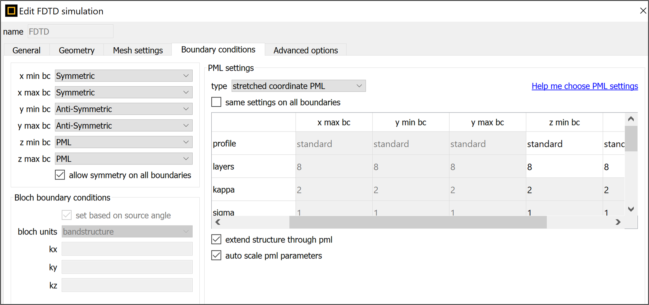
- XMIN, XMAX, YMIN, YMAX, ZMIN, ZMAX BOUNDARIES: These fields describe the boundary conditions to be applied along the perimeter of the simulation region. Symmetric and asymmetric boundary conditions should be applied to the lower boundary conditions.
- ALLOW SYMMETRY ON ALL BOUNDARIES: By default, symmetric and anti-symmetric conditions can only be used on the lower boundaries (x min, y min and z min). This box allows you to also use symmetry and anti-symmetric conditions on the upper boundaries in order to simulate periodic structures that exhibit symmetry.
- SET BASED ON SOURCE ANGLE: Bloch boundary conditions are often used to inject plane waves on angles into periodic structures. This option will determine the values kx
, ky and kz for you based on the source in your current simulation. Note that if more than one source is defined, all sources must require consistent Bloch settings. By default, this box is checked. If you uncheck the box, you should set kx, ky and kz
- directly.
- BLOCH UNITS: Two types of units are allowed for specifying the values of kx
- , ky and kz
- :
-
- bandstructure: In these units kx,y,z
- is the x,y or z span of the FDTD simulation region. These units are very convenient for bandstructure calculations.
- SI: In SI units, kx,y,z
-
- are defined in units of m-1. This is generally more convenient for the injection of plane waves on angles.
- KX, KY, KZ: The wavevector setting in the x, y and z direction for the Bloch boundary in the units specified above.
- PML SETTINGS
- TYPE: Sets the type of PML boundary formulation to be used. The options are a PML based on a stretched coordinate formulation or a PML based on a uniaxial anisotropic material formulation (legacy option).
- SAME SETTINGS ON ALL BOUNDARIES: When unchecked, this option allows users to set different PML settings for the XMAX, YMIN, YMAX, ZMIN and ZMAX boundaries. When checked, the same PML settings are used for all boundaries.
- TABLE: Sets the PML profile to be used on each boundary. The section on PML boundary conditions provides a brief description of the intended use of each profile.
- EXTEND STRUCTURE THROUGH PML: see extending structures through PML.
- AUTO SCALE PML PARAMETERS: The PML default profiles ("standard", "steep angle", etc) are tuned to provide optimal absorption per layer of PML, which will converge as the mesh size (and therefore the time step) are reduced. In some cases, the time step becomes substantially smaller than expected, typically due to a different region of very fine mesh, or because of the use of reduced "dt stability factor". The autoscaling of the PML automatically adjusts the PML parameters to account for the variation in dt, and ensures that the optimal performance of PML is maintained.
Advanced options
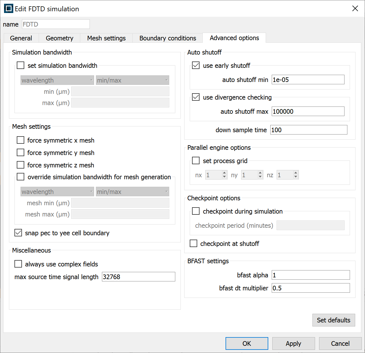
| WARNING: This tab includes options which should only be changed if you are quite familiar with the meshing algorithm and techniques used. |
Simulation bandwidth
- SET SIMULATION BANDWIDTH: By default, the simulation bandwidth is inherited from the source bandwidth. Enabling this option allows the simulation bandwidth to be set directly. Simulation bandwidth affects many aspects of the simulation including mesh generation, material fits, monitor frequency ranges, etc.
Mesh settings
- FORCE SYMMETRIC X, Y, Z MESH: This will force a symmetric mesh about the x, y or z axis. When this option is enabled, the meshing algorithm ONLY considers objects in the positive half of the simulation region. The mesh in the negative half is simply a copy of the positive half mesh. All physical structures and mesh override regions in the negative half will not be considered by the meshing algorithm. This option also forces a mesh point at the center of the simulation region. Forcing a symmetric mesh ensures that the mesh does not change when going from a simulation with symmetry to a simulation without symmetry.
- OVERRIDE SIMULATION BANDWIDTH FOR MESH GENERATION: This option allows the simulation mesh to be generated following a custom wavelength or frequency range, rather than the simulation bandwidth (which is inherited from the source by default).
- SNAP PEC TO YEE CELL BOUNDARY: This option forces any structures defined as PEC to have interfaces that are aligned with the Yee cell boundaries. This ensures that all electric field components at the PEC interface are tangential to the interface. This setting avoids complications that can result in some circumstances if normal electric field components are set to 0 at a PEC interface. To achieve this, the specified PEC interface may be shifted by as much as dx/2 when creating the simulation mesh, where dx is the size of the Yee cell.
Miscellaneous
- ALWAYS USE COMPLEX FIELDS: This checkbox forces the algorithm to use complex fields during simulation. This will result in slower simulation times and increased memory requirements and should only be used when necessary. By default, complex fields are only used when Bloch boundary conditions are present.
- MAX SOURCE TIME SIGNAL LENGTH: This is the maximum length of data used by sources to store the “time” and “time_signal” properties of sources. If a large number of sources are used and the simulation time is on the order of 100ps (which is very rare), advanced users may want to reduce this to save memory. However, since the “time” and “time_signal” properties of sources are important for calculating the sourcepower, sourcenorm, and the normalization for the transmission functions, care must be taken with source normalization. In particular, in most cases, nonorm option should be used.
Auto shutoff
- USE EARLY SHUTOFF: This will automatically end the simulation when most of the energy has left the simulation volume.
- AUTO SHUTOFF MIN: The simulation will end when the total energy in the simulation volume drops to this fraction of the maximum energy injected. The simulation data will automatically save.
- USE DIVERGENCE CHECKING: This will automatically end the simulation when the total energy in the simulation volume is this many times larger than maximum energy injected.
- AUTO SHUTOFF MAX: The simulation will end when the total energy in the simulation volume rises to this many times the maximum energy injected. The simulation data will automatically save.
- DOWN SAMPLE TIME: Check the auto shutoff conditions every down sample time number of dT time steps
Parallel engine options
- SET PROCESS GRID: The division of the simulation volume into sub-regions, which are then run as a separate processes, can be manually set for more efficient computation. Better performance will be achieved when the regions are square e.g. for 20 regions, 5x2x2 is usually more efficient than 20x1x1.
- NX, NY, NZ: The process layout for parallel simulations.
- SET DEFAULTS: Can be used to reset the settings back to their original default settings.
Checkpoint options
- CHECKPOINT DURING SIMULATION: This will create a checkpoint during simulation at intervals specified by CHECKPOINT PERIOD.
- CHECKPOINT AT SHUTOFF: This will create a checkpoint any time the simulation ends except when Quit and don't Save is selected.
BFAST settings
- BAFST ALPHA: It is the smallest dielectric refractive index in the simulation region, and should generally be 1. For example, if the background index is set to 1.33 of water in FDTD "General" tab, then 1.33 should be used here instead of the default of 1.
- DT MULTIPLIER: It is used to further reduce the time step "dt" in "Mesh settings" in addition to the "dt factor". Its largest value is 1, meaning no change for the dt factor. When it is smaller than 1, the actual time step dt becomes smaller, in some cases it can overcome some diverging problems impossible by modifying other settings.
Results returned
After the simulation has run the following results can be returned
Grid
- X, Y, Z: The mesh position vectors for the x, y and z directions.
Simulation status
- STATUS: Current status of the simulation, denoted by 0 for simulation in layout mode, 1 for run to full simulation time, 2 for run to autoshutoff, or 3 for diverged.
- AUTOSHUTOFF LEVEL: autoshutoff level vs simulation time/wall clock time
Simulation benchmark
- INITIALIZATION TIME: time to mesh and initialize in seconds
- SIMULATION RUN TIME: time to run FDTD simulation in seconds
- SIMULATION CHECKPOINT TIME: time to checkpoint simulation in seconds
- MISCELLANEOUS TIME: miscellaneous time in seconds
- SOLVER SPEED: FDTD solver speed on process 0 in Mnodes/s
- TOTAL SOLVER SPEED: total FDTD solver speed on all processes in Mnodes/s
- TOTAL PROCESSES: total number of processes
- TOTAL THREADS: total number of threads per process
| Note: These results can be copied to the script workspace using the function getresult with "FDTD" as the monitor name. For example: |
stat = getresult("FDTD","status");
Ports (FDTD) - Simulation Object
![]()
Ports can act as a combination of mode source, field monitor, and mode expansion monitor. Ports can be used alone or in conjunction with the S-parameter sweep tool to extract the S-parameters for a device by using the mode expansion method. See the "What is mode expansion" section at the bottom of this page for details on the mode expansion calculation. See Ring resonator FDTD (final parameter extraction) for an application example which uses ports and the S-parameter sweep tool.
| Note: For information on the port objects used in the Eigenmode Expansion (EME) solver in MODE, see EME Ports. |
To add a port, click on the Port button
![]()
in the main toolbar. An FDTD simulation region must be present in order to add ports. Once a port is added, a port group called “ports” is automatically added as the child of the FDTD solver region, and all port objects are contained within this group. Note that the port hierarchy is set so ports cannot be moved outside of the "ports" group, and other objects cannot be moved into the group. The name of the "ports" group also cannot be modified. However, the names of the port objects and order of the port objects inside the port group can be modified.
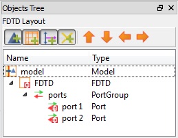
Ports
Port objects are where you can select the basis modes to be used in the S-parameter calculations described in the "What is mode expansion" section.
By default when you add a new port object, it will be set up to inject in forward x-axis direction and port will span the full simulation region span. The port that is set up to be the source will have a pink arrow in the injection direction and ports that are not injecting will have a green arrow pointing in the injection direction. In the following image, the port on the left is the source port.
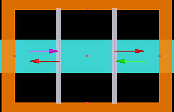
Port group
The port group object is where you can select which port and mode to use as the source in the simulation as well as set the frequency range and number of frequency points to record the field profile over. Only one port mode can be used as the source at a time so only 1 port will inject in a simulation. However, note that having the ports group enabled does not automatically disable other source objects that may be present in your simulation
Mode expansion
Consider a waveguide/fiber that supports a set of forward-propagating modes, φforward m
(with Eforwardm and Hforwardm ), and backward-propagating modes, φbackward m (with Ebackwardm and Hbackwardm
). If a complete basis state of modes is known, any input field can be expanded using these modes:
Ein=∑m(amEforwardm+bmEbackwardm)
Hin=∑m(amHforwardm+bmHbackwardm)
am
and bm
represent the complex transmission coefficient of the forward and backward propagating waves respectively. The forward and backward propagating modes are related by symmetry:
E backward m=Eforwardt,m−Eforwardz,m^z
H backward m=−Hforward t,m+Hforwardz,m^z
where we decomposed Eforwardm
in a transverse component Eforwardt,m and longitudinal component Ebackwardz,m (assuming the modes propagate in the z direction), and similarly for Hforwardm. Thus, we can rewrite the expressions above for the input fields completely in terms of forward-propagating modes and simplify the notation by dropping the forward/backward notation and using φm (with Em and Hm
) for the forward-propagating modes. If we assume power orthogonality of these modes according to
〈φm|φn〉≡0.5∗∫S⋅Em×H∗n=Nmδmn
then the coefficients for any mode m
can be determined from the overlap integrals:
0.5∗∫dS⋅Einput×H∗m=(am+bm)Nm
0.5∗∫dS⋅E∗m×Hin=(am−bm)N∗m
This is the basic concept behind mode expansion monitors. The user can specify an arbitrary input field Ein
and Hin (recorded by a frequency monitor), and modal fields Em and Hm
(by a mode expansion monitor). The mode expansion monitor will return the following results:
am=0.25∗∫dS⋅Ein×H∗mNm+∫dS⋅E∗m×HinN∗m
bm=0.25∗(∫dS⋅Ein×H∗mNm−∫dS⋅E∗m×HinN∗m)
Nm=0.5∗∫dS⋅Em×H∗m
Pin=0.5∗∫dS⋅Ein×H∗in
where Re(Nm)
is the power of the mode m in the waveguide, and Re(Pin)
is the total input power (in Watt) recorded by the frequency monitor. The script function expand can also be used to perform this type of mode expansion.
| Note: Grid dispersion These equations only apply to the ideal case. In practice, since an FDTD simulation uses a mesh, a correction step is necessary to account for the grid dispersion from this discrete mesh. This correction factor is taken into account in the mode expansion monitor built-in analysis. In the limit where the mesh size gets very very small, these equations will give the same results as the mode expansion monitor with the built-in correction. |
| Note: Power orthogonality Strictly speaking, the power orthogonality condition using the conjugated cross product above is true for the bound modes of non-absorbing waveguides. A more general orthogonality relation, valid for both absorbing and non-absorbing waveguides, is based on the unconjugated cross product: 0.5∗∫dS⋅Em×Hn=N∗mδmn |
| This approach is implemented in the script function expand2. It happens that for bound modes of non-absorbing waveguides, E and H (transverse to the direction of propagation) are real valued. Therefore the unconjugated and conjugated expressions for non-absorbing waveguides are the same, and the modes are power orthogonal. However, the disadvantage of this approach is that without the complex conjugate of the H-field, the normalization constant cannot be associated with the power carried by the waveguide modes, eg, of absorbing waveguides. |
Port group
- SOURCE PORT: Combo box allows user to choose from a list of the existing ports.
- SOURCE MODE: Combo box allows user to choose from the modes which have been selected in the SOURCE PORT. If port modes have been selected using the "user select" option in the port's "Modal Properties" tab, the modes are identified by the mode number in the mode list from the eigenmode solver used to select the modes.
- MONITOR FREQUENCY POINTS (OVERRIDE GLOBAL): Number of frequency points over the range to record E, H field profile data in the port monitor to be used in the mode expansion calculations. This is independent from the frequency points setting in the port object's "Modal properties" tab. By default, the number of frequency points from the global settings will be used.
- CALCULATE GROUP DELAY: The group delay of the device is calculated numerically using a finite difference approximation of the derivative of the phase with respect to frequency. The “fractional offset for group delay” is the fraction of the frequency that is used for the finite difference step size. If this setting is too low, the change in phase may be heavily impacted by noise. If it is too large it is possible that the phase will change by more than 2π
, resulting in an incorrect group delay calculation. Reducing this setting from the default may be required for very long devices ( 104+
- wavelengths) where the phase changes rapidly with frequency. Otherwise, the default setting should be used.
Frequency/wavelength settings
- SET GLOBAL SOURCE SETTINGS: This button opens the "Edit global source settings window" which can also be opened from the Source menu in the Main toolbar.
Geometry tab
The value of the injection axis property set in the modal properties tab will control the available spatial settings below:
- X, Y, Z: The center position of the simulation region
- X MIN, X MAX: X min, X max position
- Y MIN, Y MAX: Y min, Y max position
- Z MIN, Z MAX: Z min, Z max position
- X SPAN, Y SPAN, Z SPAN: X, Y, Z span of the simulation region
Modal Properties tab
- INJECTION AXIS: Sets the propagation axis. This setting will determine the geometry parameters that can be set under the "Geometry" tab (eg. if the injection axis is the x-axis, then the port object will have a 2D x-normal geometry).
- DIRECTION: This field specifies the direction in which the source will propagate. FORWARD corresponds to propagation in the positive axis direction, while BACKWARD corresponds to propagation in the negative direction.
- AMPLITUDE: The amplitude of the source as explained in the Units and normalization section.
- PHASE: The phase of the source, measured in units of degrees.
- MODE SELECTION: Allows users to select the modes to use for the mode expansion calculation. The "user select" option launches the eigenmode solver where the user can calculate and visualize the supported modes (see Mode analysis); use this option to select multiple modes. The eigenmode solver also provides a tool for frequency analysis (see frequency analysis).
- NUMBER OF FIELD PROFILE SAMPLES: Set to choose the number of frequency points at which to calculate the supported modes. Note that this does not have to correspond to the frequency points where the field data is measured which can be set in the port group. Linear interpolation of the calculated mode profiles between different frequency points will be automatically performed. Since the linear interpolation is typically a good approximation, few frequency points are required for accurate results.
- SELECT MODE: If the "user select" option has been chosen, this will bring up the Mode analysis tab for the user to select from a calculated list of modes. Multiple modes can be selected at once.
- VISUALIZE MODE DATA: This will bring up the Visualizer, showing all the profiles for the selected modes.
- CLEAR MODE DATA: Clears all the mode data.
Bent waveguide
When this option is checked, the Bent waveguide solver is used with the following settings.
- BEND RADIUS: Bend radius measured from the center of the port region.
- BEND ORIENTATION: Orientation of the cylindrical coordinate system used for solving for modes. See Bent waveguide solver for a detailed description with illustrations.
Rotations
This frame allows user to apply an arbitrary rotation to the calculate modes. The rotation will be rendered in the graphical CAD views.
- THETA: In 3D simulations, this is the angle of propagation, in degrees, with respect to the injection axis of the port. In 2D simulations, it is the angle of propagation, in degrees, rotated about the global Z-axis in a right-hand context, i.e. the angle of propagation in the XY plane.
- PHI: In 3D simulations, this is the angle of propagation, in degrees, rotated about the injection axis of the port in a right-hand context. In 2D simulations, this value is not used.
- OFFSET: Allows users to set an offset to the plane where the modes are calculated. This is useful for ensuring that monitors at an angle do not intersect with unwanted structures.
| Note: For best accuracy, we should place ports with rotations on a mesh cell. A useful approach is to add an override mesh region at the same position as the port, and this override region can be infinitely thin (i.e., one of the spans can be 0). |
Advanced
- AUTO UPDATE BEFORE ANALYSIS: If checked, the monitor will automatically update the chosen modes when "user select" in MODE SELECTION is selected. The monitor will find the best overlap between the chosen modes and the currently calculated modes, if there are a new set of modes. This allows users to keep track of the same chosen modes even the mode orders are switched, for example, when running a Parameter sweep over the waveguide width. This checkbox can be unselected but it has no effect if "fundamental mode", "fundamental TE mode" or "fundamental TM mode" is chosen in the MODE SELECTION dropdown list.
- MULTIFREQUENCY MODE INJECTION: If checked, the source profile will be calculated at multiple frequency points. This feature is recommended for broadband simulations. If this option is not checked, the same spatial field profile at all frequencies is injected. For single frequency simulations, when this option is checked the spectrum of the generated source pulse will not include a DC component, but the source pulse length may be longer compared to when this option is unchecked.
- NUMBER OF TRIAL MODES: The number of modes specified to look for in order to find a fundamental mode. This will affect the modes that the solver finds. If this number is too small, the desired modes may not be found. Often, setting this number to 100 modes will ensure that no physical modes have been missed. If more than 100 modes exist, then a larger number should be used if one is interested in higher order modes.
Impedance tab
Calculate characteristic impedance
By default, this option is enabled. When enabled, the Z0 characteristic impedance result will be calculated for each of the modes selected in the "Modal Properties" tab using the specified integration region settings. For more information about the characteristic impedance calculation, see Power and impedance integration.
When the CALCULATE CHARACTERISTIC IMPEDANCE box is checked, the following settings are available:
- INTEGRATION SHAPE: Options include circular, and rectangular.
- X1, X2, Y1, Y2 (or Z1, Z2) (valid for rectangular integration): defines the vertices of a rectangle over which the characteristic impedance Z0 is integrated
- CENTER X, CENTER Y (or CENTER Z), RADIUS (valid for circular integration): defines the center and radius of a circle over which the characteristic impedance is integrated
Results returned
Results are available from the individual port objects inside the Port Group.
Port modes
For the following results, the data is only available for the center freqeuncy point before running the simulation. After the simulation has been run, the data is returned as a function of wavelength or frequency.
- NEFF: Effective index of selected modes as a function of n (mode number) and wavelength or frequency.
- IMPEDANCE: Calculated characteristic impedance as a function of n (mode number) and wavelength or frequency.
- MODE PROFILES: E, H mode profiles for each selected mode and refractive index profile as a function of x, y, z position and wavelength or frequency.
Port modal expansions
- GROUP DELAY (if enabled): Provides the group delay vs wavelength and n.
- S: Complex S-parameter as a function of n (mode number) and frequency or wavelength.
For example, if port 1 at the left of the device injects the source mode in the forward direction and the S result is being calculated from the monitor at port 2 which is at the right of the device, then S from port 2 can be calculated using amonitor∗√Nmonitorasource∗√Nsource
where a and N are expansion results defined in the "What is mode expansion" section below. Note that the S-parameters are normalized by the power carried in each mode, and depending on whether the source is propagating in the forward or backward direction and the relative placement of the ports, the expansion calculation will use the appropriate a or b coefficient in the calculation of S since a and b expansion results are the forward and backward complex transmission coefficients.
- EXPANSION FOR PORT MONITOR: A set of expansion results including S (defined above), Ttotal, Tforward,Tbackward, Tnet, a,b, N, and P. Please see the "What is mode expansion" section below and the Using Mode Expansion Monitors page for more information.
Port monitor results
- E: Electric field data as a function of position and frequency/wavelength.
- H: Magnetic field data as a function of position and frequency/wavelength.
- P: Poynting vector as a function of position and frequency/wavelength.
- T: Transmission as a function of frequency/wavelength.
- FARFIELD: Farfield data can be obtained. For more information, see Far field projections.
Mesh override - Simulation Object
![]()
If multiple mesh override regions are present, the meshing algorithm will use the override region that results in the smallest mesh for that volume of space. Constraints from mesh override regions always take precedence over the default automatic mesh, even if they result in a larger mesh size.
The 'min mesh step' setting in the solver - Mesh settings tab determines the absolute global minimum mesh size allowed in the simulation. This setting takes precedence over all other mesh constraints, including mesh override regions.
General tab
The General tab includes options to override the mesh size. If multiple mesh override regions are present, the meshing algorithm will use the override region that results in the smallest mesh for that volume of space. Constraints from mesh override regions always take precedence over the default automatic mesh, even if they result in a larger mesh size.
Set maximum mesh step
Set the desired mesh size.
- OVERRIDE X/Y/Z MESH: Override the x, y, or z direction mesh settings
- dx, dy, dz: Respective maximum mesh step
Set equivalent index
Alternatively, since the mesh spacing is usually determined by the refractive index of the materials in the simulation, it is possible to set an EQUIVALENT INDEX that will be used to determine the mesh spacing. A higher index will lead to a finer mesh.
- OVERRIDE X/Y/Z MESH: Override the x, y, or z direction mesh settings
- EQUIVALENT X/Y/Z INDEX: Respective index in x, y, and z directions
Geometry tab
Directly defined
This option allows users to define the desired mesh override position and span directly.
Based on a structure
This option allows users to parametrize the mesh override position and span based on an existing structure object or structure group.
- STRUCTURE: Accepts a string input corresponding to the name of an existing structure or structure group in the object tree. The center position and the X, Y, Z spans of the named structure will be used to set the mesh override position and spans respectively.
- BUFFER: Accepts positive integer values by which the X, Y, Z MIN, and MAX positions of the mesh override region are extended outwards in all directions. This field can also be used for refining the mesh along the normal direction of 2D surface objects where the object has no thickness.
Tips for getting the actual mesh size in FDTD
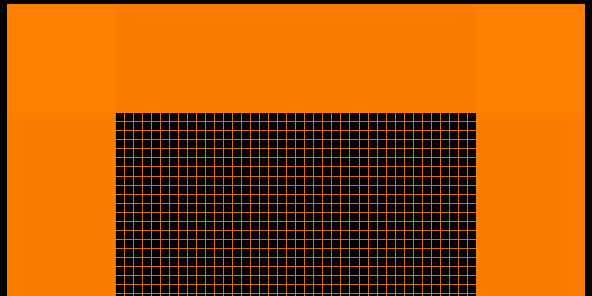
This section describes how to get the locations of the mesh points.
Measure the mesh with the ruler
The mesh can be viewed in the CAD layout editor by clicking the View simulation mesh button. The simulation mesh is not constantly updated as simulation objects are manipulated because it would make the interface too slow. The Recalculate simulation mesh (F5) button can be used to force a recalculation of the mesh.
Once the mesh is visible, the Ruler (R) mouse mode can be used to measure the mesh size. The ruler measurements are visible at the bottom of the screen.
When viewing the mesh (orange), it is often best to hide the drawing grid mesh (grey) to keep the screen from becoming too cluttered. To hide the drawing grid, click on the Edit drawing grid button, and unselect "Show grid".
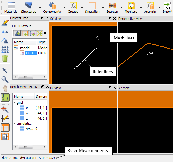
Getting the mesh from Simulation region properties
Before a simulation has been run, some information about the mesh can be obtained by getting the Simulation region properties.
addfdtd;
?getresult("FDTD","x"); # it will return the x positions of the grid points

result:
-8.5e-007
-8.10465e-007
-7.7093e-007
-7.31395e-007
-6.9186e-007
-6.52326e-007
-6.12791e-007
-5.73256e-007
-5.33721e-007
-4.94186e-007
...
...
...
Getting the mesh from monitor data
After a FDTD or propagator simulation has been run, the mesh point locations can be easily obtained from the monitor data. Generally, monitors record data at each mesh point. The getdata command can be used to get the x,y,z position vectors of the monitor data. These vectors will specify the position of each mesh point that intersect the monitor. To obtain the mesh point positions in the X,Y plane, use a 2D monitor located in the XY plane. The following script commands will get the x position vector from monitor1.
m="monitor1";  # monitor name
x=getdata(m,"x");  # x position data
Understanding Mesh Refinement and Conformal Mesh in FDTD
This page explains how conformal mesh technology can be used to improve simulation accuracy and why it is important on a finite sized mesh. For details on how to choose the best mesh refinement option for your application, please see Selecting mesh refinement options.
The conformal mesh method
The concept of the conformal mesh is to use an integral solution of Maxwell's equations near interfaces. The method used in Lumerical's software is similar to the methods described in the following publications, with some proprietary modifications:
- Yu, W., and R. Mittra, "A conformal finite difference time domain technique for modeling curved dielectric surfaces," IEEE Microwave Components Lett,, Vol. 11, 2001, pp. 25-27.
- Allen Taflove, Computational Electromagnetics: The Finite-Difference Time-Domain Method. Boston: Artech House, (2005).
- Y. Zhao and Y. Hao, “Finite-difference time-domain study of guided modes in nano-plasmonic waveguides,” IEEE Trans. Antennas Propag. 55, 3070–3077 (2007).
- A. Mohammadi, H. Nadgaran, and M. Agio, “Contour-path effective permittivities for the two dimensional finite-difference time-domain method,” Opt. Express 13, 10367–10381 (2005) .
Mesh refinement choices
To enable conformal meshing, go to the Simulation Region "Mesh settings" tab.
Please see Mesh refinement options for details on how to choose the conformal mesh settings for your application.
Maxwell's equation on a finite mesh
There are two key challenges associated with solving Maxwell's equations on a finite mesh:
- There are numerical errors associated with the finite mesh size, even in homogenous material. For example, the speed of light on a finite mesh is not the same as real space, but depends on dx, dy, dz and dt. Lumerical's graded meshing with automatic mesh generation solves this problem by adjusting the mesh to the refractive index of the materials. For example, the mesh in a material of n=2 will be twice as small as in a material with n=1, because the wavelength is smaller in the higher index material. This ensures that the numerical errors associated with the finite mesh are kept below a certain threshold in all regions of the simulation.
- It is not possible to resolve interfaces to higher precision than the size of the mesh used. One solution is to use mesh override regions to force a very small spatial mesh near interfaces. The disadvantage of this method is that it can greatly increase simulation times and memory requirements. In the FDTD method, the simulation time scales as 1/dx^4 for 3D simulations. A better solution for many applications is to use conformal mesh technology. In some cases, a combination of both solutions is required. In general, we recommend using conformal meshing as much as possible, and sometimes mesh override regions to force a smaller mesh size in critical regions.
The default conformal setting will apply conformal meshing to all materials except metals and PEC. Please see Mesh refinement options for a detailed description of the different mesh refinement options and how to choose the right setting for your application.
The figures below shows some typical structures where problems with a finite mesh size are encountered.
Example 1
Default mesh, Graded mesh
A 50nm thick layer of silicon on glass. The simulation mesh size is approximately 7nm. Without conformal meshing, the layer thickness cannot be defined to better than 7nm - in other words, a 49nm layer and a 55nm layer can give exactly the same results!
The graded mesh solution uses mesh override regions to make the mesh size 1nm at the interfaces, however many more mesh points are needed. The conformal mesh solution allows you to obtain accurate results for this type of structure without using any mesh override regions. Please note that you should see at least 2 mesh cells in your layer.
Example 2
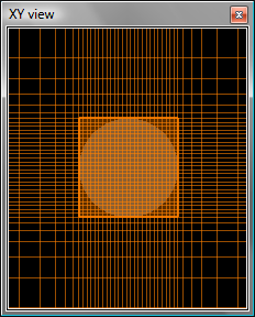
Default mesh, Graded mesh
A silver rod of diameter 50nm. In the default mesh, the curved interfaces cannot be well resolved. The graded mesh solution forces a much smaller mesh over the entire rod, introducing many more grid points.
In this application, we use a combination of graded meshing and conformal meshing. The conformal meshing can allow you to obtain more accurate results for a given mesh size. Even if the mesh size is only twice as large, for example 2nm compared to 1nm, the computation time in 3D simulations can be reduced by a factor of 16. Please take care when using conformal mesh technology with metals, however, and do some convergence testing to be sure that the conformal mesh technology is appropriate for your precise application.
Example 3
Default mesh, Graded mesh
A waveguide coupler region made from two silicon waveguides a short distance apart. The coupling length is critically sensitive to the distance between the waveguides, which can't be resolved to better than the size of dx without conformal mesh technology.
The graded mesh solution forces a much smaller mesh between the waveguides, in order to resolve the distance to any desired accuracy.
The conformal mesh solution will allow you to obtain accurate results for this type of structure without using a special mesh override region between the waveguides. Please note that the space between the waveguides should be at least 2*dx. If this is not the case, a mesh override region may be necessary to ensure this, even with the conformal mesh.
Simulation times and memory requirements
The following table shows the relationship between mesh step size and simulation time and memory requirements for 2D and 3D simulations:
| 3D | 2D | |
| Memory requirements | ∼V(λ/dx)3 |
|
| ∼A(λ/dx)2 |
| Simulation time | ∼V(λ/dx)4 |
| ∼A(λ/dx)3 |
Selecting the best mesh refinement option in the FDTD simulation object
Lumerical provides a number of mesh refinement options which can give sub-cell accuracy from a simulation. This section explains the various options and how to choose the appropriate one for your simulation. Background information can be found at Understanding Mesh Refinement and Conformal Mesh (FDTD).
How to choose which mesh refinement method to use
The default, Conformal Variant 0 setting can be used for most FDTD and varFDTD simulations. In this setting, Conformal Mesh Technology (CMT) is applied to all materials except metals and Perfect Electrical Conductors (PEC). For the purpose of this discussion, we define metals (or plasma materials) as materials with real(e) < 1 over the bandwidth of the simulation and e is the relative permittivity. The material properties in your simulation can always be viewed in the Materials Explorer.
Exceptions can be determined based on your material properties, but if options other than Conformal Variant 0 are used, careful convergence testing is highly recommended:
- If your simulation involves metals, then you may want to consider using Conformal variant 1. In this variant, CMT is applied to all materials, including metals. CMT will give better convergence than staircasing for small enough mesh sizes, but at larger mesh sizes it can sometimes give much worse results. Unfortunately, the size of a "small enough" mesh is highly dependent on the simulation. In some cases, a <5nm mesh is sufficient, while in other cases a 1nm is not sufficient (optical wavelengths). Please do some careful convergence testing between Conformal variant 0 and Conformal variant 1 to test which method you should use for your particular application. Conformal variant 1 may give numerical artifacts when |ϵplasma|>>|ϵdielectric|
- and the mesh size is not sufficiently small.
- If your simulation uses PEC instead of metals, then you will get better convergence with Conformal variant 1.
For the Eigenmode Solver in MODE, the default setting is Conformal variant 1. Since unphysical modes resulting from the possible numerical artifacts can be easily detected in modal analysis.
Note on meshing time
Any conformal meshing technique will increase the time it takes to mesh the structure prior to the simulation itself. For extremely complex structures involving many objects and large simulations the meshing time can become significant compared to the simulation time. If this is the case, you may want to return to Staircase meshing for your initial simulations and only use Conformal meshing for final results. Advanced users may also want to learn how to re-use the simulation mesh between simulations.
Special note for dipole calculations
CMT can give much better convergence for many simulations involving calculations such as Mie scattering from spheres, or reflection and transmission from multilayer stacks. However, it can also modify the local density of states. If you are doing calculations involving the power radiated by dipoles placed very small distances (10s of nm) from metal interfaces, you should compare Conformal variant 1, or Conformal variant 2 with the standard Conformal setting, which disables CMT for metal interfaces, to be sure that your results have converged.
Summary of each method
- Staircasing: The material at each position of the Yee cell is evaluated to determine which material it is in, and the E field at that location uses only that single material property. The resulting discretized structure is unable to account for structure variations that occur within any single Yee cell, resulting in a "staircase" permittivity mesh that coincides with the Cartesian mesh Furthermore, any layers are effectively moved to the nearest E field position on the Yee cell, meaning that layer thickness cannot be resolved to better than dx.
- Conformal variants: Lumerical's Conformal Mesh Technology (CMT) uses a rigorous physical description of Maxwell's integral equations near interfaces between two materials that is able to incorporate Lumerical's Multi-Coefficient Materials. The CMT can handle interfaces between arbitrary dispersive media. In general, this provides greater accuracy for a given mesh size, or make it possible to run jobs much faster without sacrificing accuracy. Due to the (1/dx)4
- dependence of the simulation time on the mesh size, results can often be achieved in roughly 1/10 the time. See Conformal Mesh Technology details below for more information. If more than two materials are found in a single cell, the method reverts to Staircasing for that cell. The Conformal meshing comes in three flavors:
- Conformal variant 0: CMT is not applied to interfaces involving metals or PEC material.
-
Conformal variant 1: CMT is applied to all materials, including PEC and metals.
-
Conformal variant 2: The Yu-Mittra method 1 (see description below) is applied to interfaces involving metals and PEC, while CMT is applied to all other interfaces.
- Dielectric Volume Average: The dielectric volume average method can only handle interfaces between one or more dielectric materials in a Yee cell. In this case, an average permittivity is created that is the simple volume average of all the dielectric permittivities in the given cell. The volume average is calculated by dividing the cell into NxN subcells in 2D and NxNxN subcells in 3D, where N is the "meshing refinement" value specified by the user. If non-dielectric materials are present at the cell center, then the method reverts to the Staircase method for that particular cell. This method has no real physical basis, but can be used for very low index contrast dielectric structures. In particular, if there is a low index contrast spatial variation in the permittivity, such as 1.4+0.01sin(x), then this method can give good results because it will average the permittivity over the entire Yee cell.
- Volume Average: The permittivity of each cell is the simple volume average of the permittivities of the 2 materials in the cell. Each material can be fully dispersive. If more than two materials are found in a single cell, the method reverts to Staircasing for that cell.
- Yu-Mittra method 1: This method was introduced by Yu and Mittra to provide greater accuracy when modeling PEC/dielectric interfaces. Lumerical's formulation is a slight extension of the original Yu-Mittra formulation that can be used with arbitrary dispersive media. In the figure below, we see the original formulation where the presence of a perfect electrical conductor (PEC) is taken into account by reducing the contour integral C to include only the region outside the PEC where the electric field is non-zero (C1). In our implementation, when updating the B field, the contour C1 is evaluated in material 1, while the contour C2 = (C-C1) is evaluated in material 2. In the event that one of the materials is PEC (where E=0), this is identical to the original Yu-Mittra formulation for PEC. If more than two materials are found in a single cell, the method reverts to Staircasing for that cell.

- Yu-Mittra method 2: This method was introduced by Yu and Mittra to provide greater accuracy when modeling dielectric interfaces. Lumerical's formulation is a slight extension of the original Yu-Mittra formulation that can be used with arbitrary dispersive media. An effective permittivity is assigned each permittivity component in the Yee cell, that is weighted by the fraction of the mesh step that is inside material 1 or material 2. If more than two materials are found in a single cell, the method reverts to Staircasing for that cell.
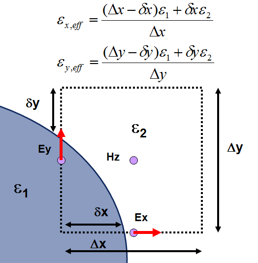
- Precise Volume Average: The precise volume average method should be used in photonic inverse design. It is a memory intensive option, but provides the most sensitive meshing to small geometric variations as required for the accurate gradients calculations used by inverse design. The average permittivity is determined by ratio of the two materials in the mesh cell using more precise techniques than volume average. The meshing refinement parameter is used to increase the accuracy of this technique. By default it is set to 5, but can be increased to 12 for the most accurate results. Photonic Inverse Design Overview - Python API
For more information on the Yu-Mittra method and other conformal mesh algorithms, see the following references:
- Yu, W., and R. Mittra, "A conformal finite difference time domain technique for modeling curved dielectric surfaces," IEEE Microwave Components Lett,, Vol. 11, 2001, pp. 25-27.
- Allen Taflove, Computational Electromagnetics: The Finite-Difference Time-Domain Method. Boston: Artech House, (2005).
- Y. Zhao and Y. Hao, “Finite-difference time-domain study of guided modes in nano-plasmonic waveguides,” IEEE Trans. Antennas Propag. 55, 3070–3077 (2007).
- A. Mohammadi, H. Nadgaran, and M. Agio, “Contour-path effective permittivities for the two dimensional finite-difference time-domain method,” Opt. Express 13, 10367–10381 (2005) .
Conformal Mesh Technology details
Motivation
In recent years, photonic design has focused on ever smaller devices expected to operate over broad wavelength ranges, and that make use of highly dispersive materials. Emerging photonic technologies including plasmonics and silicon photonics exploit dispersive material characteristics and modern semiconductor manufacturing techniques to provide new functionality to the optical designer. While such technologies open the door to greater innovation, the combination of dispersive, high index contrast materials and nanoscale feature sizes have in turn place extreme demands on commercially available photonic design tools.
Background: Conformal Mesh FDTD
While the finite-difference time-domain (FDTD) technique is ideally suited in principle to provide broadband performance data for nanoscale photonic devices, the standard Yee-cell FDTD algorithm relies on discretizing the underlying structure onto a Cartesian mesh. The resulting discretized structure is unable to account for structure variations that occur within any single Yee cell, resulting in a "staircase" permittivity mesh that coincides with the Cartesian mesh.
In general, conformal mesh methods try to account for subcell features by solving Maxwell’s integral equations near structure boundaries. For example, the Yu-Mittra method , shown in Figure 1, can be used to improve accuracy when modeling curved PEC surfaces. While this method is simple to implement, and accurately describes the interaction of electromagnetic radiation at microwave and radio frequencies with most metallic materials, it will not provide accurate results for many types of simulations conducted at optical frequencies, such as propagation through multilayer stacks of dispersive materials. Nevertheless, the Yu-Mittra method is illustrative of the approach used by all conformal meshing methods.
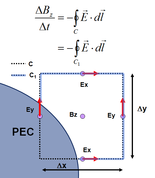
FIGURE 1. In the Yu-Mittra model, the presence of a perfect electrical conductor (PEC) is taken into account by reducing the contour integral C to include only the region outside the PEC where the electric field is non-zero (C1).
Lumerical’s Conformal Mesh Technology
At optical frequencies, the dispersive nature of commonly-used materials must be taken into account. This can be done accurately via Lumerical’s Multi-coefficient Materials (MCMs), which makes it possible to simulate highly-dispersive materials used in applications ranging from solar cells through biosensors and CMOS image sensors. Figure 2 shows common materials employed in such designs, and the types of fits that can be accomplished using MCMs.
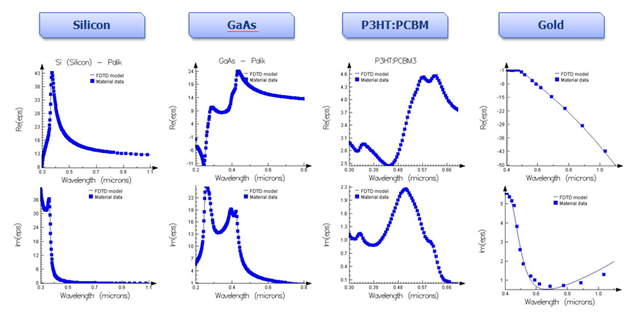
FIGURE 2. Complex permittivity of typical materials employed in current photonic designs over wavelengths ranging from the ultraviolet to near infrared, together with the fits generated by Lumerical’s MCMs.
By applying a more rigorous physical description of the conformal mesh approach, Lumerical has developed Conformal Mesh Technology (CMT) that is able to incorporate arbitrary dispersive MCMs. As an extension of general conformal mesh algorithms to handle dispersive materials, it is easily possible to generate more simple conformal mesh models like the Yu-Mittra model from Lumerical’s CMT.
CMT Capabilities
Greater Accuracy for a Coarse Mesh
Lumerical’s CMT is capable of generating significant accuracy improvements relative to staircase results. This can be illustrated by applying the CMT to a multilayer stack, which is a common element incorporated within various photonic designs. As a conceptually simple but challenging test case, we consider the reflection and transmission of non-normal incidence p-polarized light through a five layer stack which includes dielectrics, metals and semiconductors. As the analytic transmission from this multilayer stack can be easily computed with transfer matrix theory, it provides a good test case to demonstrate the ability of CMT to account for subcell features as shown in Figure 3.
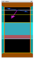
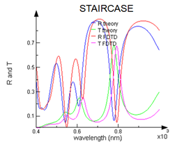
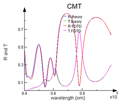
FIGURE 3. Multi-layer stack composed of gold, a constant dielectric material of index 1.9, Si, GaAs, and Ge tested over a wavelength range of 400-1000nm using a mesh resolution of 10 points per wavelength. The staircase result in (b) shows significant deviations relative to the analytic response calculated from transfer matrix theory, while the CMT result in (c) demonstrates that subcell features can be accurately accounted for.
This simple test demonstrates the ability of CMT to resolve subcell features which, in this case, is the location of interfaces that do not necessarily match the discretized mesh. Testing shows that at a mesh resolution of 10 points per wavelength, CMT provides significantly greater accuracy than the staircase results obtained at a much higher mesh resolution of 34 points per wavelength. Examination of the average error calculated for the sum of the reflection and transmission signals over the 600nm bandwidth simulated in Figure 4 shows that the level of accuracy achieved with CMT at a coarse mesh of 10 points per wavelength could not be achieved with the staircase approach at any reasonable mesh size, and likely that more than 60 points per wavelength would be required.
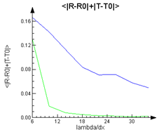
FIGURE 4. Average RMS error for reflection and transmission of five layer multilayer stack over 600nm bandwidth. The accuracy achieved by CMT at 10 points per wavelength would likely require more than 60 points per wavelength for the staircase approach.
The ability of CMT to produce much higher accuracy results with a more coarse mesh can also be demonstrated for 3D structures, like the organic solar cell device shown in Figure 5. While there is no analytic result that can be calculated for such a structure, 3D FDTD results obtained with a very fine mesh can be used in place of an analytic result. As computation time within FDTD varies with inversely with the mesh size to the fourth power (1/dx4) using a coarser mesh can result in significantly faster simulation times. For example, Figure 5 shows that the CMT can achieve the same accuracy at 14 points per wavelength as the staircase method at 26 point per wavelength, which translates into a speedup of more than 7 times.
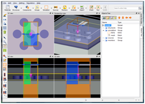
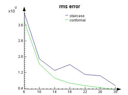
FIGURE 5. A 3D organic solar cell structure that is comprised of a periodic nanoscale pattern in a multilayer structure. By comparing staircase and CMT results against 3D FDTD results obtained using a very fine mesh, the RMS error of the two methods can be compared. To achieve a 1% RMS error, CMT requires a mesh size of less than 14 points per wavelength, while the staircase approach requires a mesh size of more than 26 points per wavelength.
Faster and Smoother Convergence
In most applications, the CMT shows faster and smoother convergence than the staircase method. This allows designers to work at coarser mesh sizes and realize the significant simulations speedups that can be obtained due to the 1/dx4 dependence of the FDTD simulation time. In Figure 6, we see the convergence of the green pixel response in a typical CMOS image sensor. The CMOS image sensor involves complex material properties, such as silicon and color filters which require the MCM to fit, AR coatings the thickness of which must be resolved to within a few nanometers, as well as curved microlens surfaces used to focus the light. The extremely quick convergence of the CMT method for this design demonstrates its robustness in a very complicated application.
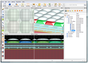
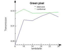
FIGURE 6. A 3D CMOS image sensor model composed of microlenses, color filters, and metallic interconnects on a multilayer substrate. The CMT allows for much faster and smoother convergence. At coarse mesh sizes, such as 6-14 points per wavelength, the CMT shows that 33% of the incident light is converted to electron/holes in the green photodiodes. The staircase method, on the other hand, may not yet be converged even at 26 points per wavelength.
Summary
The conformal mesh can enhance simulation accuracy for a given mesh size, or make it possible to run jobs much faster without sacrificing accuracy. Due to the 1/dx4 dependence of the simulation time on the mesh size, results can often be achieved in roughly 1/10 the time. Also, the CMT provides submesh sensitivity to changes in geometrical parameters, which greatly facilitates design optimization. Owing to its inherent compatibility with Lumerical’s MCMs, CMT allows designers to more efficiently prototype broadband, nanoscale photonic design concepts in high index contrast, dispersive materials.
Understanding the non-uniform mesh in FDTD
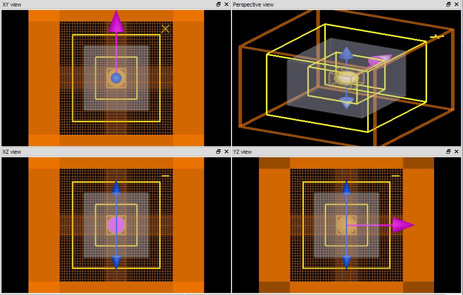
This section applies for FDTD and MODE varFDTD solver, since both use the finite-difference-time-domain method. The simulation files provided in this section are .fsp files, but the same set up can be created using MODE.
The FDTD algorithm supports a graded mesh of Cartesian (rectangular) cells. This means that the size of the mesh cells can vary as a function of position throughout the simulation region, as shown in the screenshot below. Such a non-uniform mesh can make FDTD calculations more accurate, while requiring less memory and less computation time than a comparable uniform mesh. There are two ways that the non-uniform mesh improves accuracy: through reducing numerical dispersion and improving the resolution of interfaces.
Reduced Numerical Dispersion
Numerical dispersion is an artifact resulting from the discrete spatial sampling of the FDTD mesh. This means that for a coarse mesh, the speed of light on the FDTD mesh may depart slightly from the exact value of the speed of light in the material being simulated. Furthermore, the speed of light becomes slightly anisotropic, in that it depends on the direction of propagation of the light relative to the mesh. The critical parameter that affects numerical dispersion is N = lambda_0/(n D) where lambda_0 is the free space wavelength, n is the refractive index and D is the FDTD mesh cell size. N represents the number of mesh cells per wavelength, and the numerical dispersion artifact becomes negligible as N becomes large. If the refractive index, n, is complex, then both the real and imaginary parts are considered to ensure that it has enough points per wavelength and enough points per decay length for accurate modeling.
The automesh feature automatically configures the non-uniform mesh to minimize the effects of numerical dispersion. In the usual use case, the user simply chooses a setting on the accuracy slider, which ranges in value from 1 to 8. A value of 1 creates a coarse mesh (corresponding to a small N), giving the fastest and lowest memory simulations but also introduces some (several percent) error due to the numerical dispersion artifact. At the other end of the scale, a setting of 8 creates a very fine mesh (N is large), requiring more time and memory, while ensuring that numerical dispersion is a negligible contribution to errors in virtually all situations. Simulation accuracy and computational resource requirements can be traded off in this way. For most applications, a setting of between 2 and 5 on the accuracy slider is sufficiently accurate.
Ability to accurately resolve interfaces
Many optical structures have properties that are critically sensitive to the precise locations of material interfaces. This is particularly true of structures that have resonant characteristics or high index contrast interfaces. The non-uniform mesh makes it possible to take into account the precise geometric location of these interfaces by using fine mesh cells in regions where the interfaces are important and larger mesh cells in bulk regions where there are no important interfaces as with homogeneous materials.
Lumerical provides special mesh objects termed "mesh override" objects that enable the user to indicate where the interfaces are physically significant to the problem. The automesh feature, which otherwise operates as it normally does, will then also take into account the override regions, as well as continuing to reduce numerical dispersion throughout the simulation volume. The mesh override feature is particularly useful for structures with metallic interfaces.
Boundary conditions
PML boundary conditions in FDTD and MODE
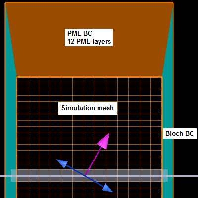
PML absorbing boundary conditions are designed to absorb incident light with minimal reflections. PML boundaries are basically implemented as an absorbing material that is also impedance matched to the surrounding materials, to minimize reflections. An ideal PML boundary produces zero reflections, however, in practice, there will always be small reflections due to the discretization of the underlying PML equations. Furthermore, as a consequence of using finite difference approximations to discretize the PML equations, there is some chance of producing numerical instabilities. The goal of this section is to outline best practices for minimizing reflection errors and getting rid of numerical instabilities without increasing simulation times unnecessarily.
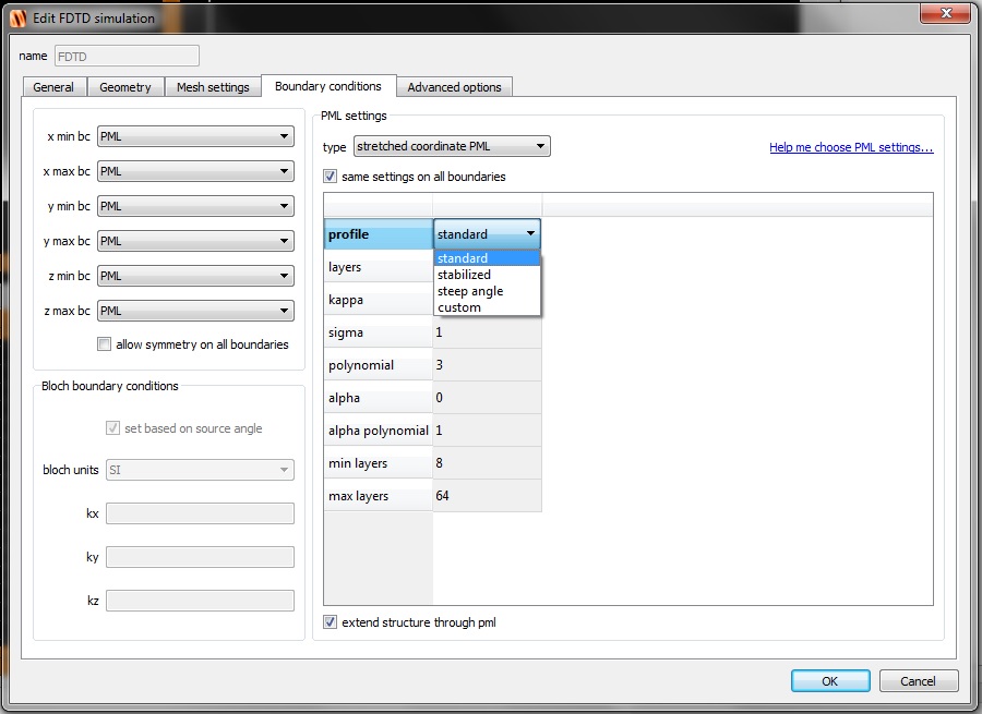
PML Type
Stretched coordinate PML (based on the formulation proposed by Gedney and Zhao [2]) is the default and recommended option. A legacy uniaxial anisotropic PML formulation is also available, but is rarely used in practice.
PML Profiles
In FDTD or varFDTD simulation regions, the user can directly specify all the parameters that control the absorption properties of the selected PML boundaries (see the screenshot on the right). To facilitate the selection of PML parameters, a number of profiles are available on the PML settings table under the boundary conditions tab. Under most simulation scenarios, the user only needs to choose one of the predefined profiles (standard, stabilized, steep angle and custom) and fine tune the number of layers. For all profiles, increasing the number of layers will usually lead to lower reflections. Having said that, each profile has a different numerical behavior and was designed with a particular application in mind.
PML Profile options
Standard
The standard profile was designed to provide good overall absorption with a relatively small number of layers. Large numbers of PML layers can significantly increase simulation times, so it is suggested to try this profile before considering any of the remaining choices. If a simulation does not contain material boundaries that cut through PML regions, this profile will almost certainly be the most sensible choice. In general, PML boundaries perform best when structures extend completely through the PML region. Whenever material interfaces cut through a PML region, it may be necessary to employ the stabilized profile.
Stabilized
When material boundaries cut through PML regions, there is some chance that numerical instabilities will appear. These usually manifest themselves as a localized exponential growth of the field amplitudes inside the PML regions (usually near material interfaces). Most numerical instabilities that can occur inside PML regions will go away with the use of this profile, however, this profile will require a higher number of PML layers than the standard profile to achieve the same absorption performance. The stabilized profile was designed to provide enhanced stability at the expense of having to increase the number of PML layers.
Steep Angle
This profile is very similar to the standard profile, and it is meant to be used when PML boundaries are combined with periodic boundary conditions. It is designed to provide enhanced absorption in situations where light travels in directions that are nearly parallel to PML boundaries. This profile is usually less absorptive than the standard profile at very coarse discretizations (less than ten points per wavelength).
Custom
The standard, stabilized and steep anlge profiles have fixed PML parameters. The custom profile allows users to experiment by giving the user full control over all the PML parameter values. The initial values of the custom profile are those of the standard profile.
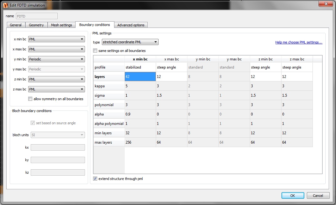
Setting PML parameters for boundaries in all diections
Using Different Profiles for Different Boundaries
PML profiles can be set individually for each PML boundary. This option can be enabled by un-checking the option "SAME SETTINGS ON ALL BOUNDARIES" at the top of the PML settings table (see the screenshot on the right). This option allows users to make changes - like increasing the number of layers - only on the boundaries that actually need them.
Using different PML profiles for different boundaries can significantly reduce simulation times. The example on the right shows the PML settings table for a 3D simulation where a stabilized profile is only needed on the x min boundary. Using the stabilized profile on all boundaries would lead to much longer simulation times, so it is recommended to increase the number of layers only on the boundaries that actually need them.
FDE vs. varFDTD and FDTD Solvers
In FDE simulation regions, the user can also specify the parameters that control the absorption properties of PML boundaries. From the onset, the FDE solver has employed a stretched coordinate PML formulation. Unlike the FDTD and varFDTD solvers, the FDE solver does not come with predefined profiles, and it employs a fixed number of layers.
PML Parameters
Unlike conventional boundary conditions, PML boundaries have a finite thickness. In other words, they occupy a finite volume that surrounds the simulation region. It is within this volume that the absorption of light happens.
- LAYERS: For discretization purposes, PML regions are divided into layers.
- KAPPA, SIGMA, ALPHA : The absorption properties of PML regions are controlled by three parameters. Their definition can be found in the second reference at the bottom of this page. Kappa is unitless by definition, but sigma and alpha must be entered into the PML settings table as normalized unitless values. Kappa, sigma and alpha are all graded inside the PML regions using polynomial functions. Parameter alpha is sometimes described as a complex frequency shift (CFS) in the reference [2]. Its main role is to improve numerical stability. Increasing the ratio alpha / sigma will make a a PML boundary more stable, but it will reduce its absorption effectiveness; this is why the stabilized profile requires a larger number of layers. To recover the S.I. unit values of alpha and sigma, it is necessary to multiply by twice the permittivity of free space and divide by the time step employed in the simulation.
- POLYNOMIAL: It specifies the order of the polynomial used to grade kappa and sigma.
- ALPHA POLYNOMIAL: It specifies the order of the polynomial used to grade alpha.
- MIN LAYERS, MAX LAYERS: They enforce a sensible range of values for the number of PML layers.
Symmetric and anti-symmetric BCs in FDTD and MODE

Symmetry boundary conditions can be used whenever the EM fields have a plane of symmetry through the middle of the simulation region. By taking advantage of this symmetry, the simulation volume and time can be reduced by factors of 2, 4 or 8.
This topic describes the difference between symmetric and anti-symmetric boundary conditions, and how to select the appropriate boundary for your simulation.
For an alternative video in Mandarin, click here
Fields at the symmetry boundary
When the EM fields have a plane of symmetry, some field components must be zero at the plane of symmetry. Symmetry boundary conditions are implemented by forcing the appropriate field components to zero. The following table lists the field components that are zero for each symmetry option.
| Symmetric Boundary | Anti-Symmetric Boundary | |
| Normal Electric Field | ZERO | |
| Tangential Electric Field | ZERO | |
| Normal Magnetic Field | ZERO | |
| Tangential Magnetic Field | ZERO |
The non-zero field components are shown in the following figure. Note that the blue arrows are electric field and the green arrows are magnetic field.

Reflection symmetry rules
The electric and magnetic fields will obey certain symmetry rules with respect to reflections through the plane of symmetry. The reflection symmetry rules are shown in the figure below.
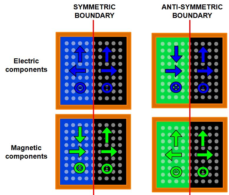
The above symmetry rules are helpful when determining the symmetry of modes found with the mode source, and resonant modes of cavities. The following figure shows the Real part of Ex and Ey of a mode that was calculated with the Mode source. The direction of propagation is +Z. Notice that Ex has the same sign on each half of the simulation region. Ey has the opposite sign on each half. Ey also goes through zero along the plane of symmetry.
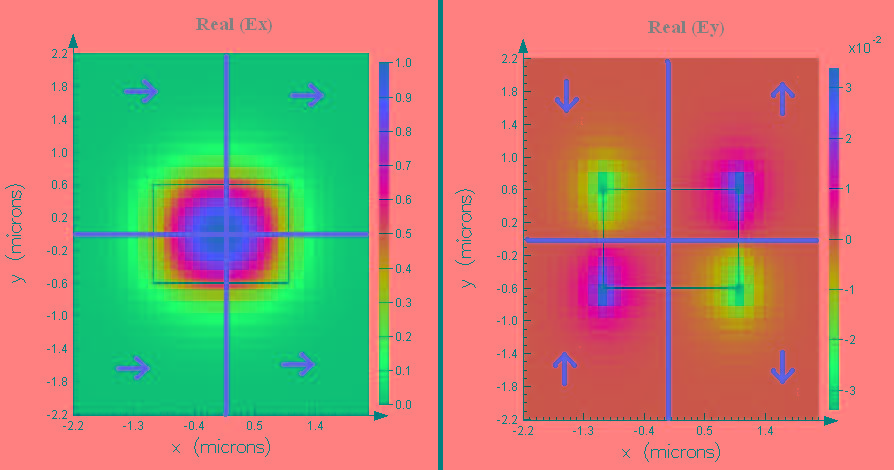
Using the above symmetry rules, we can determine that there is a plane of anti-symmetry at X=0, and a plane of symmetry at Y=0. Therefore, the x min boundary should be set to anti-symmetric and the y-min boundary condition should be set to symmetric.
Symmetric Boundary Conditions for Periodic Structures
If the EM fields through a periodic structure have a plane of symmetry or anti-symmetry in the middle of a period of the structure, then set the boundary conditions as follows:
1) select the option allow symmetry on all boundary conditions
2) set the minimum and maximum boundary conditions to be either symmetric or anti-symmetric depending on the symmetry rules given above (in practice the boundary conditions are usually either both symmetric or both anti-symmetric).
Referring to the example below, changing from Setting A to Setting B will preserve periodicity while reducing the computation time needed by about 4x. Again this only applies if the structure and fields are BOTH symmetric and periodic.
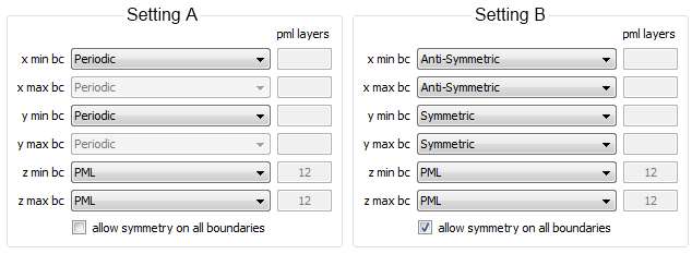
Selecting the correct symmetry option with sources
This section applies for FDTD and the MODE varFDTD solver. Most sources in these solvers show their Electric or Magnetic polarization with colored arrows, where the electric field polarization is shown in blue and magnetic polarization is green. The following image shows an electric dipole on the left and a magnetic dipole on the right. The sources use a color scheme Electric field polarization is Blue
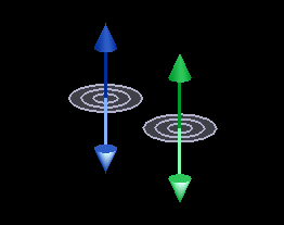
Symmetry boundary conditions use a similar color scheme:
- Symmetric BC are Blue
- Anti-Symmetric are Green.
The following figure shows how to select the correct symmetry condition based on the source polarization.
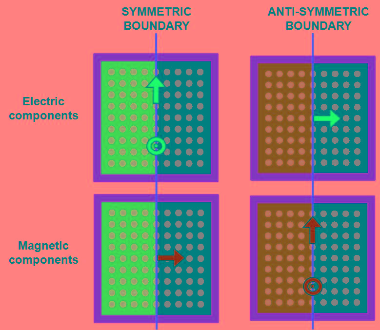
- If the source polarization is tangential to the plane of symmetry, select the symmetry option with the same color.
- If the source polarization is normal to the plane of symmetry, select the symmetry option with the opposite color.
Examples
In the following example with the triangular structure, there is one plane of symmetry in X. The source polarization (Blue) is tangential to the X boundary. Therefore, we use Symmetric for the X min boundary condition. This simulation will run 2x faster than the equivalent simulation without any symmetry settings. Notice that the blue arrow of the source is along the edge of the region with the same color.

This next example shows a simulation with two planes of symmetry (in X and Y) The source polarization (Blue) is normal to the X boundary, and tangential to the Y boundary. Therefore, use Anti-Symmetric for the X min boundary and Symmetric for the Y min boundary. The X and Y max boundary condition do not need to be modified. This simulation will run 4x faster than the equivalent simulation without symmetry boundary conditions. Notice that the blue arrow of the source is along the edge of the region with the same color, and sticking into the region with opposite color following the rules outlined above.
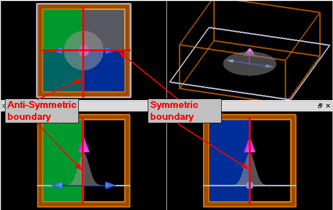
Notes
Using the wrong symmetry option
When using symmetry boundary conditions, it is easy to select the wrong symmetry option. There will be no warning message if the wrong symmetry option is selected, but the simulation results will be completely wrong. The easiest way to confirm that you have the correct option is by re-running the simulation without symmetry boundary conditions. Both simulations should give the same results. If they don't, you may have selected the wrong symmetry option.
Simulation span
Do not change the size of the simulation region when using symmetry. If symmetry boundary conditions are selected, half of the simulation region will automatically be shaded in blue or green, indicating the portion of the simulation region that will not be directly simulated.
Unfolding data
Script commands like getdata, getelectric or getmagnetic automatically unfold the field data according to the symmetry rules of the boundary condition. This makes it easy to create an image monitor the data over the entire simulation region, even though only half the simulation region was actually simulated. However, there will be no data recorded by the monitor if it is entirely in the shaded region. Some analysis group may not work when symmetry is applied but some of them contain script commands to properly unfold the field data.
Bloch boundary conditions in FDTD and MODE
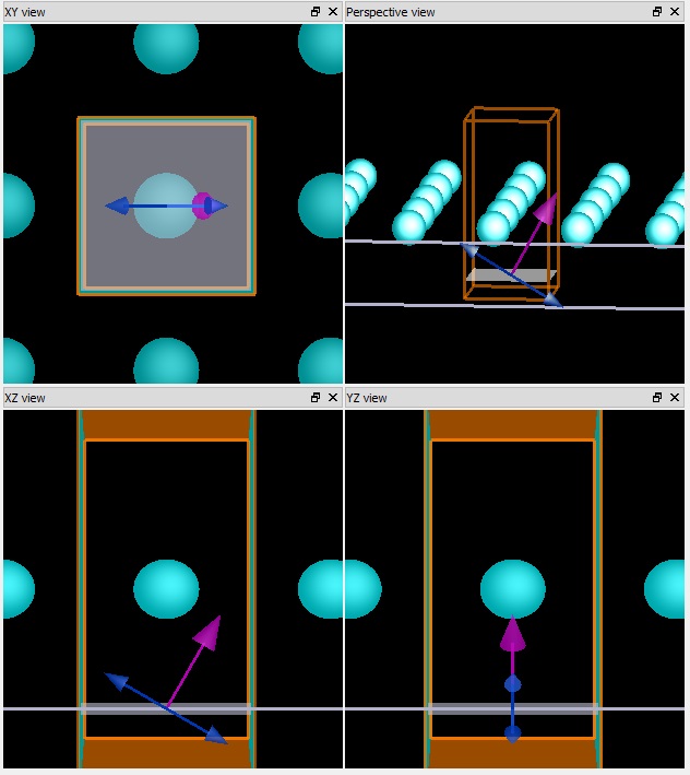
This section describes Bloch Boundary Conditions (BC's), when they are required, and how they are different from periodic BC.
Bloch boundary conditions are used in a variety of situations, but the most common is in simulations of periodic structures that are illuminated with a plane wave source propagating at an angle (as shown in the screenshot below). If a BFAST plane wave is used, this Bloch BCs are automatically overridden by use of its own built in BCs.
Periodic structures illuminated by the plane wave source
Bloch BC's are easiest to understand when compared with Periodic BC's for applications where a periodic structure is illuminated by a plane wave source, as shown in the above screenshot. Periodic BC's simply copy the fields at one edge of the simulation region and re-inject them at the other edge. Bloch BC's are very similar, but while copying the fields from one edge to the other they also apply a phase correction to the fields.
→Exmin=e−iax kblochx→Exmax
→Exmax=eiax kblochx→Exmin
The need for this phase correction is easy to understand when considering a plane wave propagating at an angle as shown in the following movies. When the propagation is at an angle, the fields from one period to the next are not exactly periodic: They will be out of phase by some amount. The Bloch BC's correct for this factor.
Movie of plane wave propagating at an angle

This simulation is setup correctly. A uniform wave front at an angle of 45 degrees is visible, as expected. Movie of Ex fields from a simulation of a plane wave propagating in the Z direction at a 45 degree angle of incidence in free space. Bloch BC's are used in the X direction.

INCORRECT! Same setup as above, but with periodic BC in the X direction. This is a common error. Periodic boundaries are not correct because kx of the plane wave is non-zero. A similar error will occur if the "set based on source angle" is not enabled. The error is visible in the scattering that occurs at the simulation boundary.
Other uses, including bandstructure calculations
Bloch BC's are useful in other situations where setting the in-plane wavevector is important. For example, they are used extensively in Bandstructure calculations.
Tips and additional information
Can Bloch BC's be used for propagation at normal incidence
Bloch BC's can be understood as a more general form of Periodic BC's. Simulations that use Periodic BC's would continue to give correct results if the Periodic BC's were replaced with Bloch BC's. In such cases, the Bloch BC's will apply a phase correction of zero degree's, which is equivalent to simply copying the fields from one edge to the other. However, as described in the Computational cost section, using Bloch BC's requires more memory and time, compared to using Periodic BC's.
Computational cost
Simulations that use Bloch BC's required up to 2x the memory and time compared to an equivalent simulation without Bloch BC's. This increase occurs because the simulation must use complex valued time domain fields, rather than the default choice of real valued time domain fields.
Implications of using complex valued time domain fields
As stated in the Computational cost section, simulations using Bloch BC's used complex valued time domain fields. In addition to increasing the computational cost of the simulation, this can affect the type of data collected by some monitors:
- Index monitors: No change.
- Frequency domain field monitors: No change.
- Time domain field monitors: Recorded data will be complex, rather than real. In some situations, having complex valued data is helpful. In situations where it is not desired, simply take the real part of the monitor data.
- Time domain movie monitors: When the 'Intensity' option is selected, movies will look slightly different. Rather than seeing every oscillation of the fields, only the envelope function will be visible. This is easy to understand in the following example:
|
The blue line shows a sin wave modulated by a gaussian pulse. The green line shows |E|^2 of this signal (Ex1 in the following code). This is what you would see in an 'Intensity' movie from a simulation using real valued fields. The red line shows |E|^2 of the complex version of this signal (Ex2 in the following code). This is what you would see in an 'Intensity' movie from a simulation using complex valued fields. # Code to reproduce figure
t=linspace(0,20,1000);
w=10;
Ex1=sin(w*t)*exp(-(t-10)^2/5);
Ex2=exp(1i*w*t)*exp(-(t-10)^2/5);
plot(t,real(Ex1),abs(Ex1)^2,abs(Ex2)^2);
legend("Real Ex","|Ex_real_field|^2","|Ex_complex_field|^2"); |
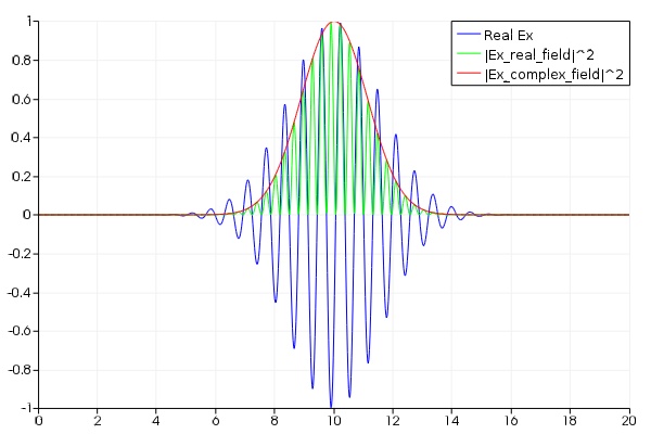
Broadband injection for sources at an angle
As explained above, Bloch BC's apply a phase correction to the fields. This has important consequences for broadband simulations, as explained on the Plane waves - Angled injection page. Additional information can be found on the Bloch BCs in broadband sweeps over angle of incidence KX page. For broadband angled injection, the BFAST plane wave is recommended.
Automatic calculation of the Bloch vector when using the plane wave source
When doing simulations that involve Bloch BC and plane waves at an angle, "set based on source angle" option should be enabled (it is by default), as shown in the following figure. This setting is only accessible when using Bloch BC. If you disable this option, you have to input kx, ky, and kz manually. Manually setting the bloch vector is important for bandstructure simulations.
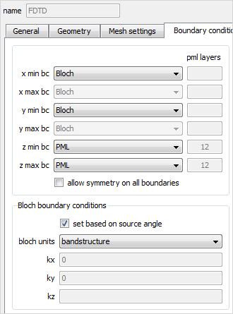
| Note: When using multiple plane wave sources and Bloch BC in the simulation, all sources should have the same bandwidth and angle. If not, a warning will be shown and the Bloch vector will be set to 0.
|
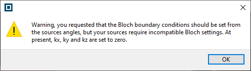
Edge Effects to the Mesh
When simulating periodic, or uniform structures that intersect the Bloch BCs it is important to be careful with how the edges of the structure are being meshed. As described in this article the BC will always be one mesh cell thick, the inner FDTD boundary is used for the calculations; however, if the structure doesn't extend through this BC the structure can be meshed incorrectly. The easiest solution is to extend the structures through Bloch mesh cell.
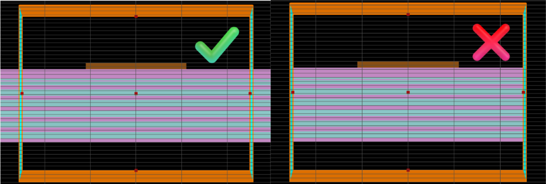
This can be cryptic because even with the default setting of the index monitor this anomaly will not be visible. It can be visualized by changing the the spatial interpolation in the index monitor to 'none', or 'nearest mesh cell'.
Periodic boundary conditions in FDTD and MODE
When studying periodic systems, Periodic BC's allow you to calculate the response of the entire system by only simulating one unit cell. Periodic BC's are relatively straightforward to use in your simulation: simply set the simulation span to be one unit cell wide and select Periodic BC's for that boundary. When the simulation runs, the Periodic BC's simply copy the EM fields that occur at one side of the simulation and inject them at the other side.
The most important detail to remember is that when using Periodic BC's, everything in the system must be periodic: both the the physical structure AND the EM fields. A common source of error is to use periodic boundary conditions in systems where the structure is periodic, but the EM fields are not. Examples include:
- A periodic structure is illuminated by a plane wave propagating at an angle. The fields will not be quite periodic in this case, as there will be a phase difference between each period of the device. Use Bloch BC's instead.
- A periodic structure is excited by a single dipole source, such as in OLED simulations. In this case the system is not periodic because there is only one dipole, not one dipole per period.
Movie of Ex fields from a simulation of a plane wave propagating in the Z direction at normal incidence in free space. Periodic BC's are used in the X and Y directions.

Additional Tips
- Periodic BC's are most often used with the planewave source.
- If the Plane wave source is injecting at an angle, then the fields will not be periodic (there will be a phase difference between each period). Use Bloch BC's instead to get single frequency result, or use BFAST to get broadband result.
- For systems that are both periodic and have symmetry, select symmetry (or anti-symmetry) on both boundaries. This allows you to simulate only 1/2 of one unit cell. See Symmetric and anti-symmetric BCs for details.
- For best performance, enough of the structure should be drawn in the CAD so that it extends through the boundary condition region (the one mesh cell thick boundary region drawn in a light blue color. This ensures that the material properties are correctly defined in the boundary condition region.
- PML boundaries are typically used on the 'non-periodic' boundaries (the Z direction in the above video). The 'Steep angle' PML profile is recommended for periodic simulations because the structure can scatter light at steep angles.
Import
The import button includes options to import from a variety of formats:
Importing and exporting GDSII files
Import: The GDSII import simulation object
![]()
allows you to import structures from a GDSII file into the layout editor. The GDSII file format is commonly used to store 2-dimensional geometric data. This data can be directly imported into a 2D layout environment, or it can be used to import 3D objects into a 3D layout environment by extruding the 2D data in the Z dimension.
Export: An example can be found on the GDSII export automation and GDSII real example page. Users may also find the built-in Layer builder function useful when importing and exporting GDS files.
Characteristics of the GDSII file
Lumerical products support most, but not all features of the GDSII file format. Unsupported features should not prevent the file from being imported, however, the results may not be as expected. The following table details the supported and unsupported features.
| Features | Supported |
|---|---|
| General | |
| Multiple cells in GDSII library file | Yes |
| Layer numbers for drawing objects | Yes |
| Primitives/Objects | |
| Box/Rectangle | Yes |
| Polygon | Yes |
| Path | Yes |
| Node | No |
| Text | Yes |
| Symbolic cell reference | Yes |
| Array cell reference | Yes |
| Advanced | |
| Cell references in external library/file | No |
| Magnifications in array and symbolic references | Yes |
| Rotations and mirroring in array and symbolic references | Yes |
Note: Path corners
Path objects in GDSII files are piecewise linear lines plus a width and optionally some information on how to handle corners and ends. In general, GDSII files support several types of corner style options (squared, rounded, extended squared, etc). Our import function supports type 0 (squared ends flush to the end-point) and will default to type 2 (square ends with 1/2 the width added to the end-point) for all other types.
Note: Flattened GDSII files
While we do include scale, rotate, flip, and automatic flattening of references, not all features of GDSII are currently supported. If you run into any problems, you may have better results by flattening the file first.
GDSII file import
Import using GUI
GDSII import is initiated by accessing the IMPORT->GDSII option from the FILE menu, or by pressing the Import GDS button
![]()
located on the main toolbar. This will bring up a standard file browser, which will allow you to select a file with the extension .gds or .db. Selecting a GDSII file will bring up the Single layer GDSII Import window as shown below. A downloadable associated file GDS_export.gds can be used to test the GUI import function.
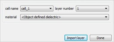
The following 3 input parameters control how the GDSII data is imported:
- Cell name: This selection menu contains the valid cells available in the GDSII library. Select the cell you wish to import.
- Layer number: This selection menu contains all of the layer number present in the GDSII file. Only structures with the selected layer number will be imported by this operation.
- Material: This selection menu contains a list of the valid materials in your current simulation environment. This material will be assigned to the imported structures.
Selecting the Import layer button imports all the structures with the selected layer number in the selected cell into the layout environment. These structures are automatically inserted into a structure group. The material is set as an input parameter for the structure code, and the script in the structure group sets all the objects to the desired material. The name of the structure group includes the original number of layers. For 3D simulations, the structure group contains a variable "z span". This used to set the width of the layer in the z direction. The origin of the structures, as well as their orientation, can be changed by changing the properties of the structure group.
In the simple ' GDS_export.gds ' example file, valid cell/layer combinations with structure information are:
Substrate / Layer 1
Si_polygon / Layer 2
Au_particle / Layer 3
Au_particle_array / Layer 3
Import using script command
The GDSII file can also be imported via script, the command gdsimport can be used, see stage 3 of the associated files GDS_export_import.lsf for example. For more information of the script commands, please visit List of commands .
GDSII file export
To export a graphical design to .gds format, the following commands can be used, see stage 2 of the associated file GDS_export_import.lsf for example.
gdsopen, gdsclose, gdsbegincell, gdsendcell, gdsaddcircle, gdsaddpoly, gdsaddrect, gdsaddref
The graphical information can be exported to the a .gds file in the current working directory. For more information of the commands, please visit Reference Guide - List of commands.
To automate the GDSII file export process, please visit the KB page GDSII export automation and GDSII real example
STL import - Simulation object
FDTD MODE DGTD CHARGE HEAT FEEM
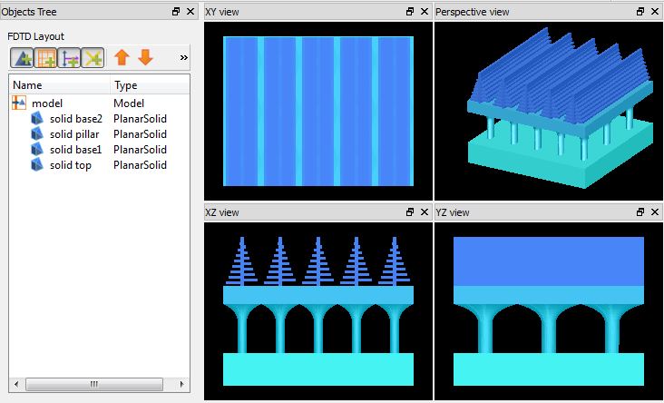
STL (Standard Tessellation Language or STereoLithography) is a well-supported format for many 3D CAD products. It is widely used for rapid prototyping and computer-aided manufacturing. STL files describe the surface geometry of 3D objects by triangular representation of the objects. The surface of the objects are broken into a series of triangles. Each triangle is uniquely defined by its three vortices and the surface-normal vector.
STL files can be imported by selecting 'File' --> 'Import' --> 'STL'. Multiple STL objects, as shown below, can also be imported by sequentially importing each file. Once imported, the STL-imported objects are treated as planar solid objects in the layout editor.
The associated files below can be used to test the import. When imported, the assembly is recognized as a single object. Alternatively, each part can be separately imported and assembled in the layout editor. In this case, each part imported is treated as a separate object.
| Notes:
|
Geometry tab
- X, Y, Z: The relative position of imported object from the origin of the layout editor.
Material tab
The material options are as follows:
- MATERIAL: This field can be set to any material included in the material database. It is possible to include new materials in the database, or edit the materials already included. See the material database section for more information.
- OVERRIDE MESH ORDER FROM MATERIAL DATABASE: Select to override the mesh order from the material database and manually set a mesh order. The mesh order is used by the simulation engine to select which material to use when two materials overlap. See the mesh order (optical) or mesh order (electrical) section for more details.
- MESH ORDER: Set the mesh order in this field if the OVERRIDE MESH ORDER FROM MATERIAL DATABASE option is selected. If the option is not selected, the field displays the material's default mesh order from the database. For example, a material of mesh order 1 will take precedence over a material of mesh order 2.
The following only applies to MODE and FDTD:
If <Object defined dielectric> is selected, then the INDEX property must be set.
- INDEX: The refractive index of the structure, when the material type is <Object defined dielectric>. The index must be greater than one.
-
-
- Anisotropic index: To specify an anisotropic refractive index, use a semicolon to separate the diagonal xx,yy,zz indices. Eg. 1;1.5;1
- Spatially varying index: It is possible to specify a spatially varying refractive index by entering an equation of the variables x,y,z in this field. Eg. 2+0.1*x will create an object where the refractive index increases in the X direction. The units of the spatial variables (x,y,z) must be set with the 'INDEX UNITS' property described below. The variables x,y,z will be zero in the center of the object. When using an equation in this field, consider using a mesh override region to control the simulation mesh size. For more information on entering equations, see the Equation interpreter section.
-
- INDEX UNITS: Only relevant when specifying a spatially varying equation in the INDEX properly described above. Specify the units (nm, um, m) of the x,y,z position variables.
- GRID ATTRIBUTE NAME: Enter the name of the grid attribute that applies to this object, see the grid attribute section
The following only applies to CHARGE, HEAT, FEEM, DGTD:
If the material chosen from the drop down menu is a binary alloy consisting of two semiconductors, then there will be an additional property, namely, the "composition fraction" to set as well.
COMPOSITION FRACTION: This is x, the fraction of the semiconductor in the alloy. x can either take a fixed value or vary.
The user can see which semiconductor has fraction x and which has fraction (1-x) shown in a line above this drop down menu.
FIXED: This means that fraction x will be a constant value between 0 and 1.
LINEAR X/Y/Z: This means that the composition fraction x will vary as a function x or y or z. In this case, user can specify the min and max fraction values for the min and max spatial points and the fraction will be interpolated linearly in between. x,y,z here are those of the unrotated object. x,y,z are local to the object.
EQUATION: The user can enter an equation for the fraction that varies with u,v and w. u is (x-x0), v is (y-y0) and w is (z-z0) where x0, y0 and z0 are the center coordinates of the object. This means that u,v and w are local to the object.
Rotation tab
Rotate objects by setting the following variables:
- FIRST, SECOND, THIRD AXES: Select rotation axis. Up to three different rotations can be applied.
- ROTATION 1,2,3: The rotation of the object in a clockwise direction about each axis, measured in degrees.
Graphical Rendering tab
The graphical rendering tab is used to change how objects are drawn in the layout editor. The options are:
- RENDER TYPE: The options for drawing the objects are detailed or wireframe. Detailed objects are shaded and their transparency can be set using OVERRIDE COLOR OPACITY FROM MATERIAL DATABASE.
- DETAIL: This is a slider which takes values between 0 and 1. By default it is set to 0.5. Higher detail shows more detail, but increases the time required to draw objects. This setting has no effect on the simulation.
- OVERRIDE COLOR OPACITY FROM MATERIAL DATABASE: When unselected the opacity is determined from the material database. When selected, you can specify a value for ALPHA between 0 (transparent) and 1 (opaque) for the object, depending on how transparent you want the object to be.
Surface import - Simulation object
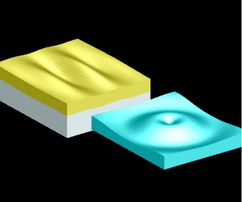
This section describes the data format for importing surface data Z(x,y) into the import primitive. It provides example data files and example script files that generate the data files. This object is sometimes used to import atomic force microscope (AFM) data.
File formats
The file formats are shown in the following tables. Spaces, commas or tabs can be used as separators in the files. The columns do not have to be aligned. Please note that as shown below, the data ranges go from 0 to m for x (0 to n for y). This means that there are actually m+1 data points in x and n+1 data points in y.
Z = Z(x,y): It is often easy to reverse the meaning of x and y when exporting a file. The surface import window provides a check button to invert x and y to correct this problem easily.
| Description | File format |
|---|---|
| type 1: The x and y data is contained in the file. An example file is usr_surface_3d_1.txt. A script file that generates this example is usr_surface_3d_1.lsf. |
|
| type 2: The x and y data is not contained in the file. An example file is usr_surface_3d_2.txt. A script file that generates this example is usr_surface_3d_2.lsf. |
|
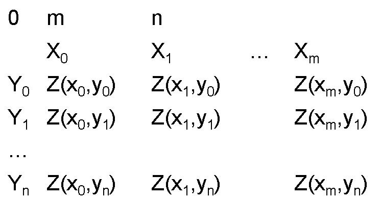
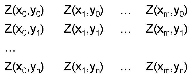
Surface object import
Using GUI
To import surface data, click on the Surface option
![]()
of the Import button in the main toolbar, which will open the Surface data import wizard.
|
|
|
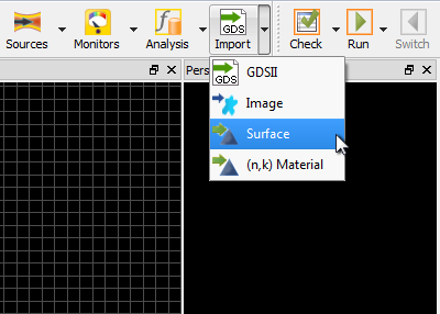
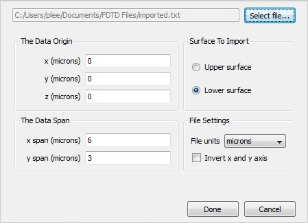
- SELECT FILE: let the user specify the data file to be imported.
- X, Y, Z: the data origin in the global coordinates of the Graphical Layout Editor. For example, if you are importing a surface defined by an AFM that is on a slab of Si that ranges from 0 to 2 microns, you should set z0 to 2 microns.
- X SPAN, Y SPAN: This defines the size of surface area that you are importing. If the x and y data was contained in the file (file format type 1), then these fields are inactive. If the x and y data was not in the file, then these fields are active and should be set to the desired data span.`
- UPPER SURFACE, LOWER SURFACE: Choose which surface is being imported.
- FILE UNITS: Select units for the data in your file.
- INVERT X AND Y AXIS: It is often easy to invert the x and y axis when exporting the file. Selecting this checkbox means that the x and y axes are automatically reversed.
| Note: importing surfaces for 2D simulations or other orientations (eg. X(y,z) or Y(x,z)) The import object always creates a surface as a function of x,y. If you need the a different surface orientation (such as when running 2D simulations which are oriented in the XY plane), use the object rotation property to rotate the object into a different plane. |
After surface data has been imported, the Import data tab allows the following properties to be modified:
- IMPORT: You can import new data into the object, or clear the imported data via a simple GUI. For properties of the import GUI, see bottom of page.
- X,Y FINE SCALE ADJUSTMENTS: Re-scale the object X,Y span. Modifying these properties will change the X,Y span properties. Z SCALE property not used for surface import.
- DATA SIZE: These properties provide some information about the imported data. They are read-only.
- LOWER, UPPER REF HEIGHT: Set the vertical location of the reference plane (height=0 in the imported data). Modifying these properties will change the Z, Z span properties.
Using Script
The following script commands are described in detail in the Scripting chapter. Examples script files are provided here.
| Command | Example files | Description |
|---|---|---|
| importsurface | usr_surface_3d_1.txt usr_surface_3d_1.lsf | Import surface data from a file created by usr_surface_3d_1.lsf |
| importsurface2 | usr_surface_3d_2.txt usr_surface_3d_2.lsf | Import surface data from script variables |
| Note: Related properties It is important to notice that the 'x, y scale' and 'x, y span' properties are linearly related. Doubling the object 'x span' will automatically double the 'x scale' property. Similarly, the 'lower, upper ref height' properties are related to the 'z and z span' properties, although the relationship is slightly more complex. See the following figure for details. The surface's can be truncated by setting the 'z span' property to a small value. |
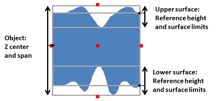
| Note: Overlapping surfaces If the z span is small enough such that the upper and lower surfaces overlap (as shown below), no structure will be included in the simulation in that region. |
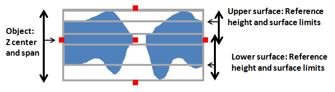
Spatial (n,k) data - Simulation object
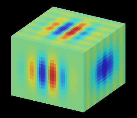
This section describes the data format for importing n and k (anisotropy possible, 2D and 3D) as a function of volume into the import primitive. It also provides example data files and example script files that generate the data files. There are two ways to import the nk data, 1) from data stored in a text file, 2) from matrices created by script commands. The imported nk data is only for a single frequency.
File formats (isotropic and anisotropic)
The file formats are shown in the following tables. Spaces, commas or tabs can be used as separators in the files. The columns do not have to be aligned. For 2D data, it will need at least 2 data points in the z direction, ie, p=2.
| Description | File format (isotropic) | File format (anisotropic) |
|---|---|---|
| type 1: Only the real part of the index is included in the file. The values of x range from X1 to Xn, y from Y1 to Ym and z from Z1 to Zp. X1 must be the minimum X value and Xn is the maximum value. Also, the values of x, y, and z must be uniformly spaced - see above note. |
|
|
| type 2: The imaginary part of the index (k) is included in the second column of the file after the header. An example file is usr_importnk_3d.txt. A script file that generates this example is usr_importnk_3d.lsf |
|
|
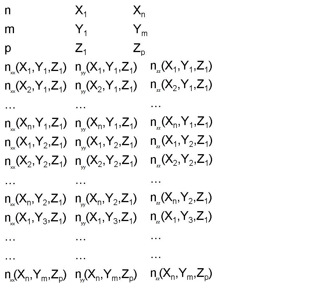
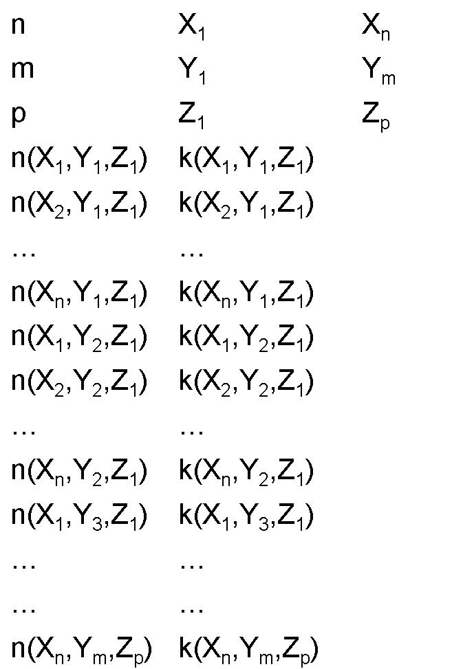
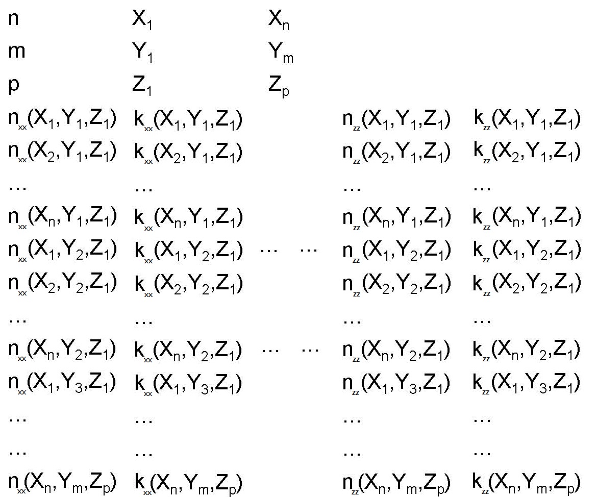
n and single frequency k import GUI
To import n,k data, click on the (n,k) Material option of the Import button in the main toolbar, which will open up the import wizard.
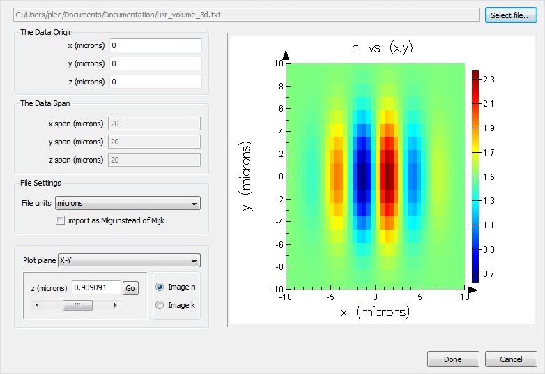
The different fields are
- SELECT FILE: let the user specify the data file to be imported.
- X, Y, Z: the data origin in the global coordinates of the Graphical Layout Editor. If you defined your volume with respect to a particular point in space, for example (0,0,-5) microns, then you should set z0 to -5 microns.
- X SPAN, YSPAN, ZSPAN: This defines the size of volume that you are importing. These fields are inactive and help to determine that the file units have been properly chosen.
- FILE UNITS: Select units for the data in your file.
- IMPORT AS Mji INSTEAD OF Mij: 2D simulation only. It is often easy to cycle through the array indices in the wrong order when exporting the file, and this check button allows you to reverse the order easily. Typically, it is very easy to see in the figure window when you have the order incorrect.
- IMPORT AS Mkji INSTEAD OF Mijk: It is often easy to cycle through the array indices in the wrong order when exporting the file, and this check button allows you to reverse the order easily. Typically, it is very easy to see in the figure window when you have the order incorrect.
- PLOT PLANE: You can image the data in either the x-y plane, the x-z plane or the y-z plane to be sure that it is correctly imported. Use this menu chooser to switch between planes.
- Z (or X or Y): Depending on the PLOT PLANE chosen, you can view cross sections at any depth into the structure. Use this slider or the value input field to choose the depth of cross section.
- IMAGE N, IMAGE K: Choose to view n or k in the figure window.
Importing n and k data using script commands
The following script commands are described in detail in the Scripting chapter. Examples script files are provided here.
| Command | Example files | Description |
|---|---|---|
| importnk | usr_importnk_3d.fsp usr_importnk_3d.lsf usr_importnk_3d.txt | Import n and k data from a file. |
| importnk2 | usr_importnk_3d.fsp usr_importnk2_3d.lsf | Import n and k data from script variables |
Visualizing the anisotropy
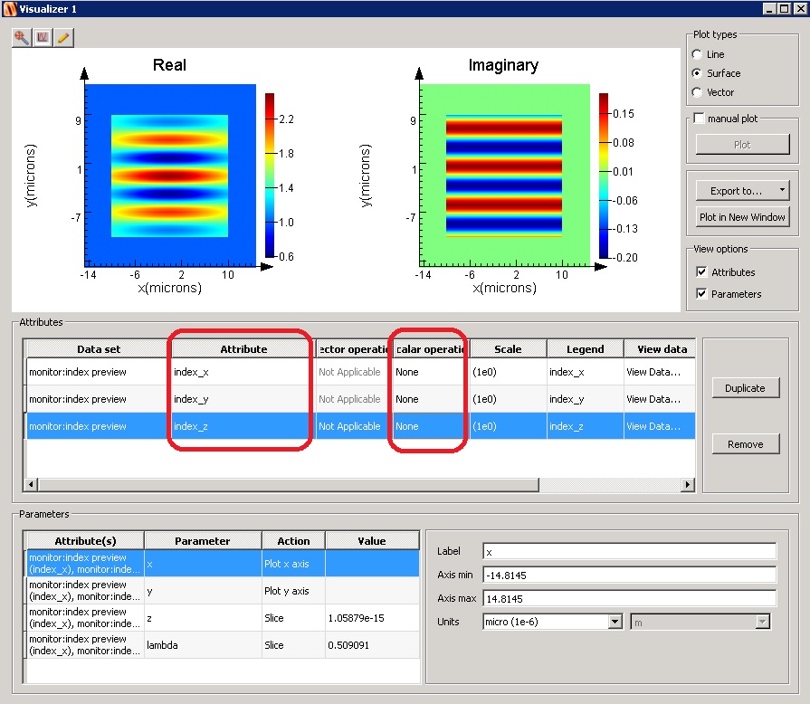
By default, only the xx-index is shown in the CAD and the import wizard. Use an index monitor to see indices in other direction.
Binary spatial data - Simulation object
This section describes the data format for importing binary data to define an object. In this binary import, the data should have values of 1 or 0, indicating that the object is or is not present.
File formats
The file formats are shown in the following tables. Spaces, commas or tabs can be used as separators in the files. The columns do not have to be aligned.
| Description | File format |
|---|---|
| The values of x range from X1 to Xn, y from Y1 to Ym and z from Z1 to Zp. The values of x, y, and z must be uniformly spaced. The number n should be either 1 (the material is present at this location) or 0 (the material is not present). If other values are used, any non-zero value will be interpreted to be 1. Note that there must be at least 2 data points in each dimension (ie, n, m, p >= 2). |
|

Binary import window
To import binary data, click on the Binary import option of the Import button in the main toolbar, which will open up the import wizard.
A screenshot of the wizard is shown in the following figure
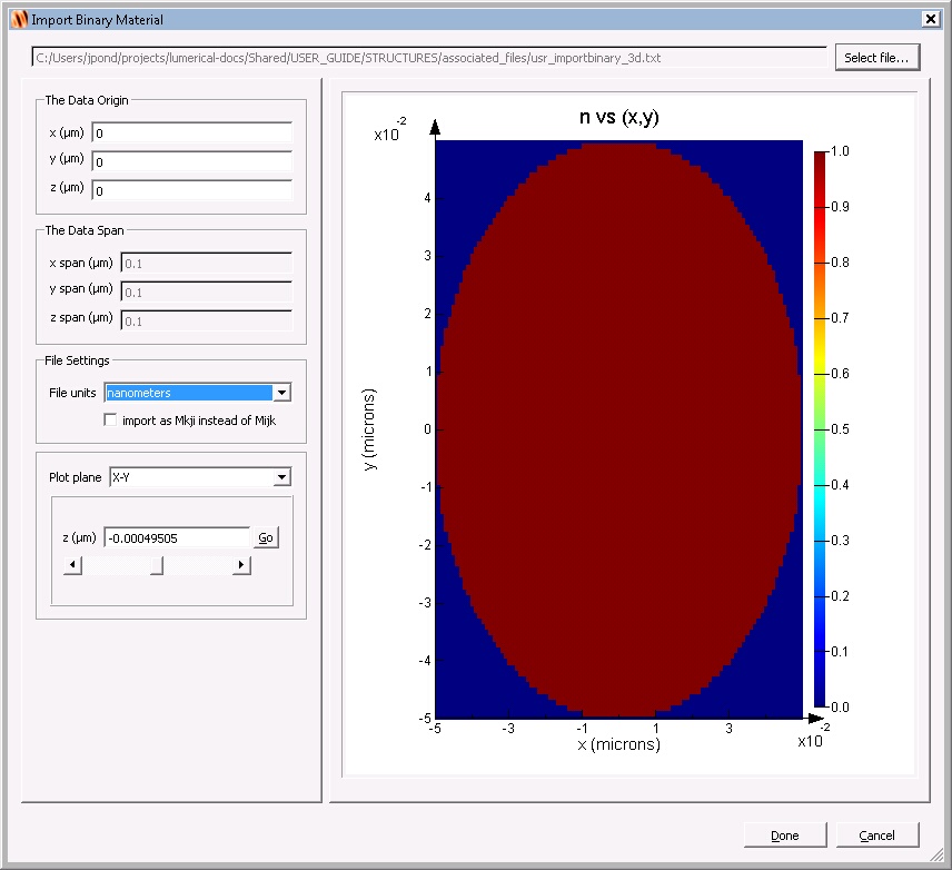
The different fields are
- X, Y, Z: the data origin in the global coordinates of the Graphical Layout Editor. If you defined your volume with respect to a particular point in space, for example (0,0,-5) microns, then you should set z0 to -5 microns.
- X SPAN, YSPAN, ZSPAN: This defines the size of volume that you are importing. These fields are inactive and help to determine that the file units have been properly chosen.
- FILE UNITS: Select units for the data in your file.
- IMPORT AS Mkji INSTEAD OF Mijk: It is often easy to cycle through the array indices in the wrong order when exporting the file, and this check button allows you to reverse the order easily. Typically, it is very easy to see in the figure window when you have the order incorrect.
- PLOT PLANE: You can image the data in either the x-y plane, the x-z plane or the y-z plane to be sure that it is correctly imported. Use this menu chooser to switch between planes.
- Z (or X or Y): Depending on the PLOT PLANE chosen, you can view cross sections at any depth into the structure. Use this slider or the value input field to choose the depth of cross-section.
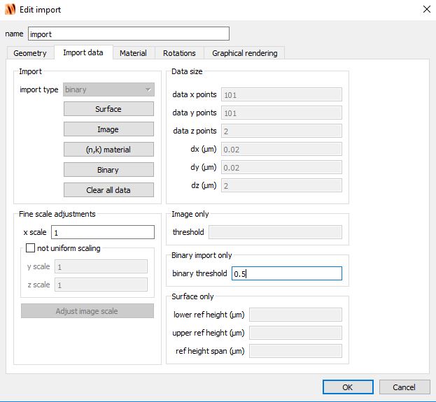
BINARY THRESHOLD: This property can be set between 0 to 1 to define the object's edge. By default, it is set to 0.5 which means that as the binary data (0 or 1) is interpolated onto the current mesh, any point that has a value of 0.5 or larger is considered "inside" the object. This default value can be the best setting for curved surfaces such as spheres.
Importing binary data using script commands
The following script commands are described in detail in the Reference Guide. Example script files are provided here.
| Command | Example files | Description |
|---|---|---|
| importbinary | usr_importbinary_3d.fsp usr_importbinary_3d.lsf usr_importbinary_3d.txt | Import binary data from a file. |
| importbinary2 | usr_importbinary_3d.fsp usr_importbinary2_3d.lsf | Import binary data from script variables |
| NOTE: Imported binary object boundaries The boundary of the import binary object is positioned between the vertices where the material is present and the vertices where the material is not present. The shape of this implied boundary can be complex, and the viewport does not show the full detail. The boundary can be moved closer to vertices where the material is present by increasing the "binary threshold" property of the import object. To confirm the boundary that will be used in the simulation by the solver, use an index monitor. |
Example:
The following lines of script will generate a simple binary object and visualize the actual boundary in an index monitor as shown below. You can see that the actual boundary (right) is not represented by the layout editor window (left).
x = [-3e-6;3e-6];
y = [-2e-6;2e-6];
z = [-1e-6;1e-6];
X = meshgrid3dx(x,y,z);
Y = meshgrid3dy(x,y,z);
Z = meshgrid3dz(x,y,z);
binary = zeros(2,2,2);
binary(1,1,1) = 1;
binary(2,1,2) = 1;
addimport;
importbinary2(binary, x, y, z);
addfdtd;
set("x span", 10e-6);
set("y span", 10e-6);
set("z span", 10e-6);
addindex;
set("monitor type","3D");
set("x span", x(2)-x(1));
set("y span", y(2)-y(1));
set("z span", z(2)-z(1));
visualize(getresult("monitor","index preview"));

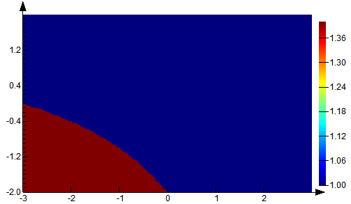
Image import - Simulation object
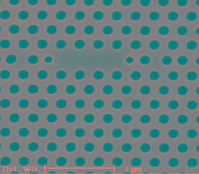
This section describes how to use the import object to create structures from an image. Images can be imported from JPG (*.jpg) or PNG (*.png). Other image types can be exported to these two formats in most image editing software.
Selecting the Import Image button in the main toolbar will open the Image Import Wizard. The wizard provides a simple interface to import, threshold, crop and scale the image. The image is used to define the objects shape in the XY plane. The object is extruded in the Z direction.
Image Import wizard
STEP 1: Add import object with the image import wizard.
A) Click on the Import button expansion arrow in the main toolbar and select the Image option to open the Image import wizard.
B) Click "Select Image" to choose your image file
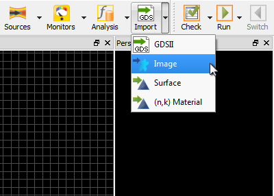
STEP 2: Set threshold
The import process takes a color or grayscale image and converts it into a binary representation of the structure. The threshold which defines what portion of the image will be set to be the background index of the simulation region is defined with the THRESHOLD slider.
The “invert” button can be used to invert the image
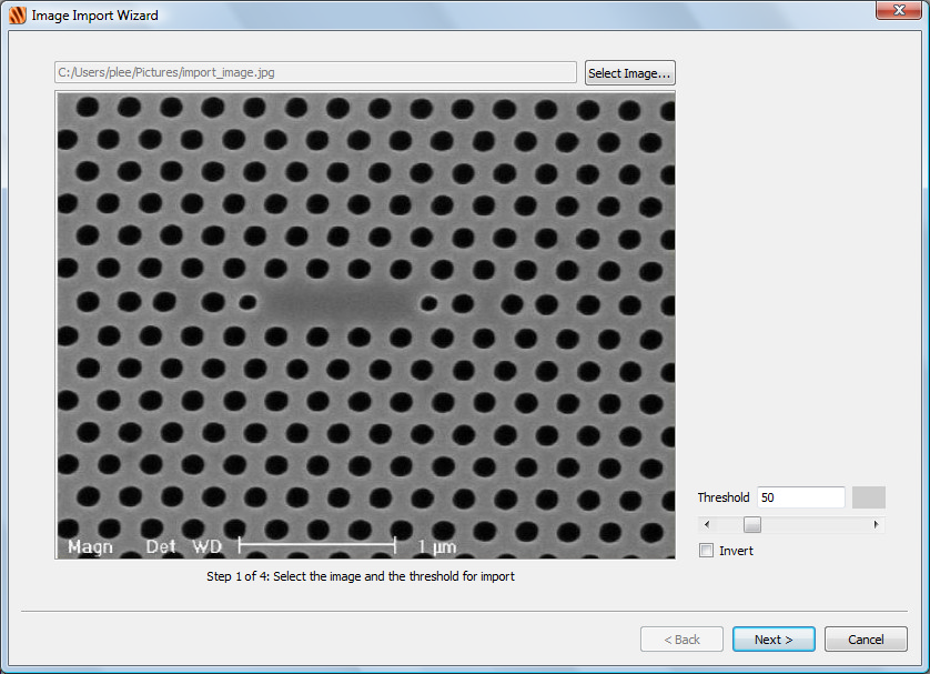
STEP 3: Set scale
Once the image has been imported, it is necessary to calibrate the length of the structure.
Here, with GRAPH CONTROL selected, the user can drag a rectangle and use the horizontal, vertical, or diagonal dimension of the rectangle to define the size of the imported structure.
For this example, we use the fact that the period is 270nm, or that 10 periods is 2.7 microns.

STEP 4: Crop image
With the “crop image” and “crop” items selected, the image can be cropped using the mouse to define a rectangular region.
Once a rectangle has been dragged within the plot area region, its edges can be dragged to the correct location.
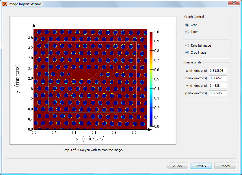
STEP 5: Review result
The last step of the import wizard allows you to accept the structure as depicted, or move back through the steps to make modifications.
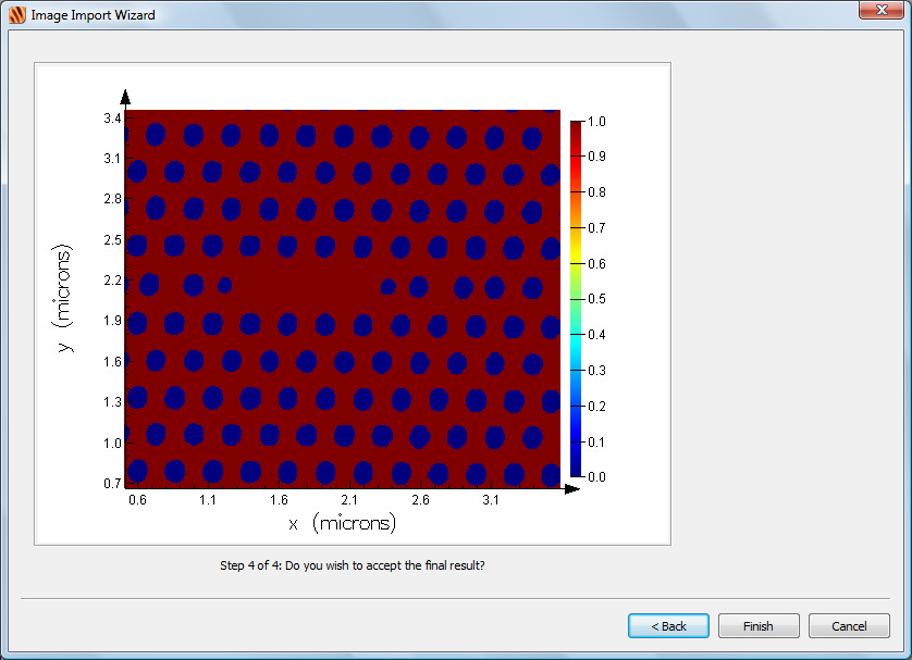
STEP 6:
See imported object in the CAD layout editor.
When the image import wizard is finished, you will see the imported object in the CAD layout editor.
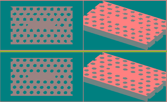
Note: Drawing resolution
Initially the object will be drawn at a low resolution, as shown in the top half of this figure. You can increase the drawing resolution with the settings on the Graphical rendering tab. The bottom half of this figure shows the object displayed at the same resolution as the image that is was imported from. It is important to note that the graphical rendering does not affect the simulation. Irrespective of the drawing resolution, the meshed object used for the simulation is always as has been defined.
Fine scale adjustment
In order to open up the wizard to adjust the fine scale, click on the "Adjust image scale" button in the "Import data" tab of the import object's edit window as shown below.
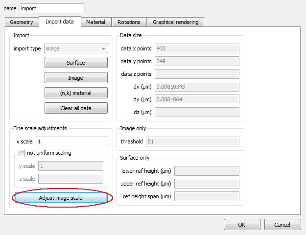
STEP 1: Verify settings
Drag the ruler to a desired horizontal, vertical or diagonal length. Check that the distance from A-B is what you expect.
Verify lengths in at least 2 different directions.
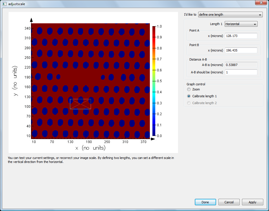
STEP 2: Define one length
Choose a direction to recalibrate your scale, for example, horizontal. Drag the ruler over a known length, enter the “distance A-B should be” setting and hit Apply. The distance A-B will now be precisely what you defined.
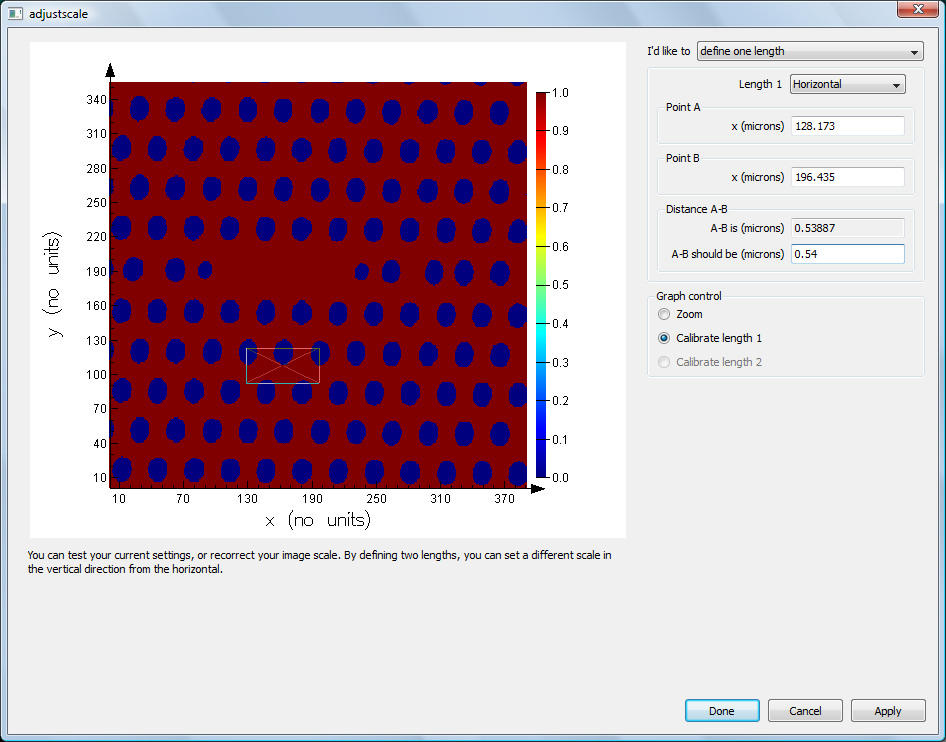
STEP 3: Define a second length
Verify that your structure has the correct length in a direction different to the one used in STEP 2. If the length is not correct, choose to “define two lengths”. Select “calibrate length 2” and drag the ruler to define a second length, for example, diagonal. Enter the desired distance A-B for the second length and hit Apply. You can now verify that both lengths are correct.
Hit Done when you are satisfied with your calibration. The x scale and y scale settings will be automatically updated to reflect your desired changes.
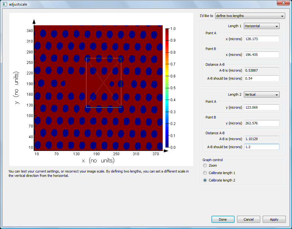
Import liquid crystal orientation from CSV - Simulation object
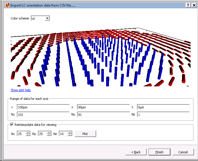
This section describes how to use the CSV import to directly import spatial Liquid Crystal (LC) orientation data from a CSV (comma-separated value) file. This file is typically created with TechWiz LCD from Sanayi System Co., Ltd. (사나이시스템) and makes it easy to import spatial information on LC orientation from TechWiz LCD simulations.
| Note: Other methods to define spatially-varying LC The required CSV file format is not simple to generate yourself, so data that is not already in the required format can be imported using the addgridattribute and importdataset script commands instead. See LC rotation for more information about adding spatially-varying LC grid attributes. |
The file format for the CSV file that defines the LC orientation as a function of space can be in a 2D format or 3D format.
File format
2D format
The file should have the form:
THETA,X=-50,X=-49,X=-48,X=-47,X=-46,X=-45,X=-44,X=-43,X=-42,X=-41,X=-40,X=-39,X=-38,...

Y=1,90,90,90,90,90,90,90,90,-,-,90,90,-,-,…

Y=2,45,45,35,25,-,-,-,-,25,…

….


PHI,X=-50,X=-49,X=-48,X=-47,X=-46,X=-45,X=-44,X=-43,X=-42,X=-41,X=-40,X=-39,X=-38,...

Y=1,35,45,55,65,75,85,90,90,-,-,90,90,-,-,…

Y=2,11.5,15.2,20,30,-,-,-,-,30,40,…

….
Where
- The orientation of the LC is defined by THETA and PHI.
- PHI is the azimuthal angle in the X-Y plane with respect to the x-axis, in degrees, using a clockwise rotation when looking down the z-axis
- THETA is the angle between the x-y plane and the LC, in degrees. The polar angle, measured from the z-axis, is 90-THETA, in degrees.
- The Ux, Uy, and Uz components of the unit orientation vector of the LC is given by
- Ux = sin(90-THETA)*cos(-PHI)
- Uy=sin(90-THETA)*sin(-PHI)
- Uz=cos(90-THETA)
- When THETA or PHI are given by “-”, it indicates that there is no LC at that grid location
- The units of X and Y are always in micrometers (microns)
- There are precisely 2 sections, one for THETA and one for PHI
- The same values of X and Y are repeated in each section
- Each section has the same number of values of X and Y as columns and rows for THETA or PHI
3D format
The file should have the form:
THETA

Z=0,X=0,X=1,X=2,X=3,…

Y=1,90,90,90,90,90,90,90,90,-,-,90,90,-,-,…

Y=2,45,10,22.5,15.7,-,-,-,-,75,…

….


PHI

Z=0,X=0,X=1,X=2,X=3,…

Y=1,0,0,0,0,90,90,90,90,-,-,90,90,-,-,…

Y=2,13.4,10.5,3.23,15.7,-,-,-,-,75,73,…

….

THETA

Z=1,X=0,X=1,X=2,X=3,…

Y=1,75,75,75,90,90,90,90,90,-,-,90,90,-,-,…

Y=2,45,10,22.5,15.7,-,-,-,-,75,…

….


PHI

Z=1, X=0,X=1,X=2,X=3,…

Y=1,10,20,30,0,90,90,90,90,-,-,90,90,-,-,…

Y=2,13.4,10.5,3.23,15.7,-,-,-,-,75,73,…

….


…………
Where
- The orientation of the LC is defined by THETA and PHI.
- PHI is the azimuthal angle in the X-Y plane with respect to the x-axis, in degrees, using a clockwise rotation when looking down the z-axis
- THETA is the angle between the x-y plane and the LC, in degrees. The polar angle, measured from the z-axis, is 90-THETA, in degrees.
- The Ux, Uy, and Uz components of the unit orientation vector of the LC is given by
- Ux = sin(90-THETA)*cos(-PHI)
- Uy=sin(90-THETA)*sin(-PHI)
- Uz=cos(90-THETA)
- When THETA or PHI are given by “-”, it indicates that there is no LC at that grid location
- The units of X and Y are always in micrometers (microns)
- There are an equal number of THETA and PHI sections. The number of values of Z is equal to the number of THETA (or PHI) sections.
- The same values of X and Y are repeated in each section
- The same value of Z is repeated in each pair of THETA and PHI sections
- Each section has the same number of values of X and Y as columns and rows for THETA or PHI
Graphical import
Opening the wizard
The CSV import feature is accessible from the import toolbar with the menu item “Import from CSV”.
This will open the CSV import wizard where you can import any CSV file described in the file format section. The import wizard has three pages.
Page 1
This page allows you to select a file. Press the browse button get a file browser for easier selection.
Page 2
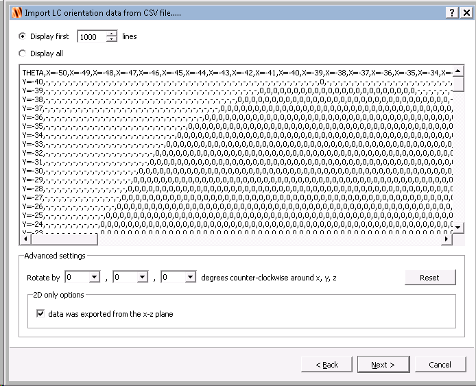
The file display
This page displays the CSV file, and you can control the amount of the file viewed. For larger files, it may not be desirable to preview the entire file.
The advanced settings and rotations
- Optionally, rotations in increments of 90 degrees around the x, y, and z axes may be performed. For example, if the exported format was in the x-y plane while the user desires the structure to be in the x-z plane, a 90-degree rotation around the x-axis can be used. This rotation applies to both the spatial location and the LC orientation.
- For 2D data sets, the user can indicate that the data was originally exported from the x-z plane (even though in the CSV file, the axes are specified as 'X' and 'Y'). This is critical to obtain the correct orientation of the LC with respect to the x-y plane that will be used in FDTD. However, if 2D data is actually exported from the x-y plane then this should be unchecked.
Page 3

The color scheme
The color scheme setting can be used to make the arrows appear blue when they are oriented with a particular axis. For example, if the color scheme is set to "uz", the arrows will be blue if they are in the +z direction, green if they are at 45 degrees to the z-axis, and red if they are in the x-y plane.
The plot control
The plot allows for full zooming and rotation in 3D. Click the Show plot help link to expand the plot help and see all the possible controls.
Range of data for each axis
This displays the actual span of data for each axis and the number of data points that were imported. Note that you may see fewer cylinders displayed because some of the imported locations may have been set to "-" in the file, and a cylinder will not be drawn at that location.
Reinterpolate data for viewing
The user can interpolate the data for better viewing. This is particularly useful when the data is defined over a region with a large aspect ratio or for large files.
Scripted import
The importcsvlc script command can be used to import the LC information from the CSV file from the script without using the GUI import wizard.
Imported object
The CSV data is imported into a group object that contains Lumerical’s “grid attribute” and a rectangle. The rectangle is transparent for better viewing. The properties of the imported LC including position, scaling, resampling for viewing, and the LC material can all be set directly by the “LC” analysis group. The names of the LC material and LC attribute can be changed directly in the tree view. If desired, the grid attribute can be removed from the group for association with more complex physical geometries. Also, when scripted import is used, it is possible to import only the grid attribute for association with more complex physical geometries.
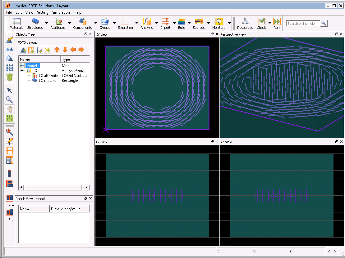
The following properties can be edited directly in the analysis group called "LC".
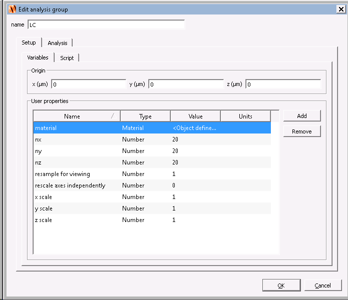
Please note that the corresponding properties should not be edited directly in the "LC attribute" child or the "LC material" child objects as they will immediately be overwritten by the "LC" analysis group.


 245
245

 被折叠的 条评论
为什么被折叠?
被折叠的 条评论
为什么被折叠?
 到【灌水乐园】发言


