


- 引脚图
- 简化版,引脚逻辑图(抄PPT的
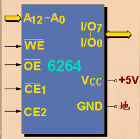
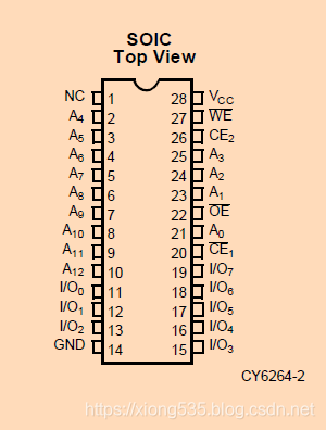
引脚功能:
- A 12 − A 0 A_{12} - A_0 A12−A0,13根地址线,选择芯片内 2 13 2^{13} 213 个存储单元中的任一个单元。
- I / O 7 − I / O 0 I/O_7-I/O_0 I/O7−I/O0, 8根双向数据线,并行传送8位读/写数据
- W E ‾ \overline{WE} WE 写入允许信号,低电平有效。
- O E ‾ \overline{OE} OE 读出允许信号,低电半有效。
-
C
E
1
‾
,
C
E
2
\overline{CE_1},CE_2
CE1,CE2 片选信号,两者均为低电平时才能对芯片进有读/写操作。
- Functional Description
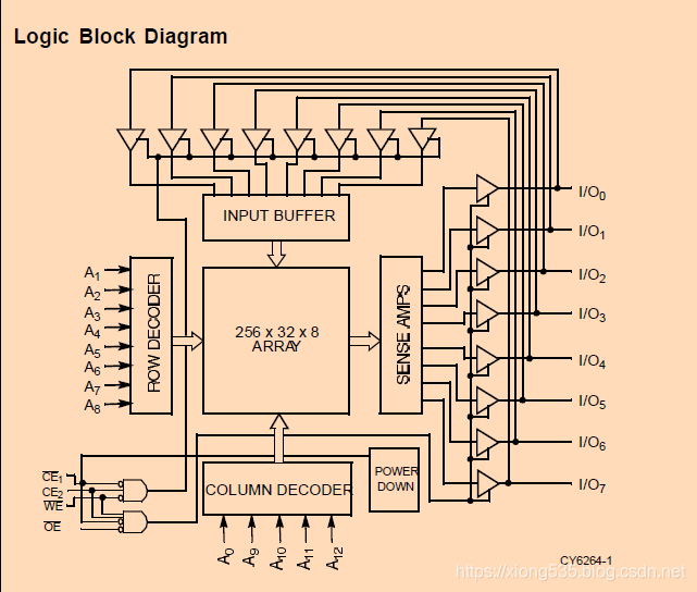
The CY6264 is a high-performance CMOS static RAM orga-nized as 8192 words by 8 bits. Easy memory expansion is provided by an active LOW chip enable (CE1), an active HIGH chip enable (CE2), and active LOW output enable (OE) and three-state drivers. Both devices have an automatic power-down feature (CE1), reducing the power consumption by over 70% when deselected. The CY6264 is packaged in a 450-mil (300-mil body) SOIC.An active LOW write enable signal (WE) controls the writing/reading operation of the memory. When CE1 and WE in-puts are both LOW and CE2 is HIGH, data on the eight data input/output pins (I/O0 through I/O7) is written into the memory location addressed by the address present on the address pins (A0 through A12). Reading the device is accomplished by selecting the device and enabling the outputs, CE1 and OE active LOW, CE2 active HIGH, while WE remains inactive or HIGH. Under these conditions, the contents of the location addressed by the information on address pins is present on the eight data input/output pins.The input/output pins remain in a high-impedance state unless the chip is selected, outputs are enabled, and write enable (WE) is HIGH. A die coat is used to insure alpha immunity.


 1234
1234

 被折叠的 条评论
为什么被折叠?
被折叠的 条评论
为什么被折叠?
 到【灌水乐园】发言


