


目录
5 bit LFSR
A linear feedback shift register is a shift register usually with a few XOR gates to produce the next state of the shift register. A Galois LFSR is one particular arrangement where bit positions with a "tap" are XORed with the output bit to produce its next value, while bit positions without a tap shift. If the taps positions are carefully chosen, the LFSR can be made to be "maximum-length". A maximum-length LFSR of n bits cycles through 2n-1 states before repeating (the all-zero state is never reached).
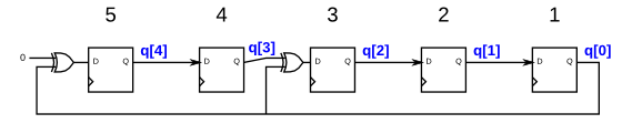
The following diagram shows a 5-bit maximal-length Galois LFSR with taps at bit positions 5 and 3. (Tap positions are usually numbered starting from 1). Note that I drew the XOR gate at position 5 for consistency, but one of the XOR gate inputs is 0.
Module Declaration
module top_module(
    input clk,
    input reset,    // Active-high synchronous reset to 5'h1
    output [4:0] q
);
线性反馈移位寄存器是通常带有几个XOR门的移位寄存器,用于产生移位寄存器的下一个状态。 Galois LFSR是一种特殊的移位寄存器,其中将带有“抽头”的位位置与输出位进行异或运算以产生其下一个值。 如果仔细选择抽头位置,则可以将LFSR设为“最大长度”。 n位的最大长度LFSR在重复之前循环经过2n-1个状态(永远不会达到全零状态)。
下图显示了一个5位最大长度的Galois LFSR,在位置5和3处有抽头(抽头位置通常从1开始编号)。 请注意,为保持一致性,我在位置5处绘制了XOR门,但XOR门输入之一为0。
说到底,就是一个移位寄存器,只不过某些输入不是上一级触发器的输出,而是有可能和其他级的输出进行了异或作为当前的输入;
给出设计(与0异或等于本身):
module top_module(
    input clk,
    input reset,    // Active-high synchronous reset to 5'h1
    output reg [4:0] q
);
    always@(posedge clk) begin
        if(reset) q <= 5'h1;
        else begin
           // q[4] <= q[0];
           // q[3] <= q[4];
           // q[2] <= q[3]^q[0];
            //q[1] <= q[2];
            //q[0] <= q[1];
            q <= {q[0],q[4],q[3]^q[0],q[2:1]};
        end

    end


endmodule
3 bit LFSR
Module Declaration
module top_module (
	input [2:0] SW,      // R
	input [1:0] KEY,     // L and clk
	output [2:0] LEDR);  // Q
下面对上面的电路进行设计:
首先,可以看出有三个类似的模块可以调用,那就描述出来这个子模块如下:
module sequential_com(
	input clk,
	input in1,
	input in0,
	input sel,
	output q
	);

	wire in_sel;
	assign in_sel = sel ? in1 : in0;

	reg q_mid = 0;
	always@(posedge clk) begin
		q_mid <= in_sel;
	end
	assign q = q_mid;

endmodule
例化该子模块得到顶层设计:
module top_module (
	input [2:0] SW,      // R
	input [1:0] KEY,     // L and clk
	output [2:0] LEDR);  // Q

    sequential_com isnt0(
        .clk(KEY[0]),
        .in1(SW[0]),
        .in0(LEDR[2]),
        .sel(KEY[1]),
        .q(LEDR[0])
    );

    sequential_com isnt1(
        .clk(KEY[0]),
        .in1(SW[1]),
        .in0(LEDR[0]),
        .sel(KEY[1]),
        .q(LEDR[1])
    );

    sequential_com isnt2(
        .clk(KEY[0]),
        .in1(SW[2]),
        .in0(LEDR[1]^LEDR[2]),
        .sel(KEY[1]),
        .q(LEDR[2])
    );


endmodule
32 bit LFSR
Build a 32-bit Galois LFSR with taps at bit positions 32, 22, 2, and 1.
第一题就写了5 bit的LFSR,这一题只不过多了几位,且告诉你抽头在32, 22, 2, and 1,这几个位置,请设计电路?
如何做这个题目呢?
其实很简单,先写一个位数少的,找下规律,就可以了:
module top_module(
    input clk,
    input reset,    // Active-high synchronous reset to 32'h1
    output [31:0] q
);

    reg [31:0] q1;
        always@(posedge clk) begin
            if(reset) q1 <= 32'h1;
        else begin
            q1 <= {q1[0],q1[31:23],q1[0]^q1[22],q1[21:3],q1[0]^q1[2],q1[0]^q1[1]};
        end

    end
    assign q = q1;

endmodule


 1297
1297

 被折叠的 条评论
为什么被折叠?
被折叠的 条评论
为什么被折叠?
 到【灌水乐园】发言


