


Consider the n-bit shift register circuit shown below:考虑下图所示的n位移位寄存器电路。
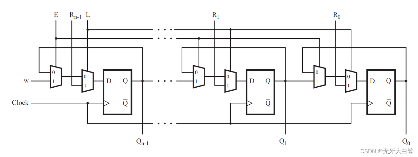
Write a top-level Verilog module (named top_module) for the shift register, assuming that n = 4. Instantiate four copies of your MUXDFF subcircuit in your top-level module. Assume that you are going to implement the circuit on the DE2 board.假设n=4,为移位寄存器编写一个顶级Verilog模块(名为top_module)。在你的顶层模块中实例化四个MUXDFF子电路的副本。假设你将在DE2板上实现该电路。
- Connect the R inputs to the SW switches,
- clk to KEY[0],
- E to KEY[1],
- L to KEY[2], and
- w to KEY[3].
- Connect the outputs to the red lights LEDR[3:0].
(Reuse your MUXDFF from exams/2014_q4a.)
通过实例数组实现,子模块是根据 exams/2014_q4a 写的。
module top_module (
    input [3:0] SW,
    input [3:0] KEY,
    output [3:0] LEDR
); //
    reg [3:0] rQ;
    MUXDFF MUXDFF_U [3:0]
    (
        .clk({KEY[0],KEY[0],KEY[0],KEY[0]}),
        .w({KEY[3],rQ[3],rQ[2],rQ[1]}),
        .R(SW[3:0]),
        .E({KEY[1],KEY[1],KEY[1],KEY[1]}),
        .L({KEY[2],KEY[2],KEY[2],KEY[2],}),
        .Q(rQ[3:0])
    );
    assign LEDR = rQ;
endmodule
module MUXDFF (
    input clk,
    input w, R, E, L,
    output Q
);
    reg rd1;
    reg rd2;

    always @ (posedge clk)
		begin
        	Q <= rd2;
        end
    assign rd1 = E? w:Q;
    assign rd2 = L? R:rd1;
endmodule


 178
178


 被折叠的 条评论
为什么被折叠?
被折叠的 条评论
为什么被折叠?
 到【灌水乐园】发言


