


位运算符
~   按位取反
&   按位与
|   按位或
^   按位异或
^~  按位同或(异或非)
除了对变量的具体位做运算,也可对整个变量进行操作,相当于将变量的每一位加到相同的与或异或同或门上
例:HDLBits 39 Gates100 要求对100位的输入建立与、或、异或门,此时可通过位运算符对整个变量作用来实现功能。
/*
Build a combinational circuit with 100 inputs, in[99:0].
There are 3 outputs:
out_and: output of a 100-input AND gate.
out_or: output of a 100-input OR gate.
out_xor: output of a 100-input XOR gate.
*/

module top_module(
    input [99:0] in,
    output out_and,
    output out_or,
    output out_xor
);
	assign out_and=∈
    assign out_or=|in;
    assign out_xor=^in;
endmodule
位拼接运算符
{}
{}={}
在进行向量拼接并进行赋值时,只需保证两边的位长相等即可,括号中的变量不需要一一对应
例:HDLBits 17 vectorr 要求对8位输入翻转输出,则左侧括号需要写出全部从0~7位(逆序),右侧(正序)则直接放上变量即可
/*
Given an 8-bit input vector [7:0], reverse its bit ordering.
*/

module top_module(
    input [7:0] in,
    output [7:0] out
);
    // this is fine, but the one below is better
    // assign {out[7],out[6],out[5],out[4],out[3],out[2],out[1],out[0]}=
    // {in[0],in[1],in[2],in[3],in[4],in[5],in[6],in[7]};
    assign {out[7],out[6],out[5],out[4],out[3],out[2],out[1],out[0]}=in;
endmodule
此外,在进行复制操作时,每个部分都需要用额外的括号包裹,如把三个in的最高位和三个in连接:
{ {3{in}},3{in[7]} }或非和异或
{}
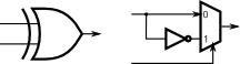
{}={}或非是NOR,或后取反,只有全0才为1
异或是XOR,相同为0,不同为1
异或门也可以实为一个特殊的数据选择器——在控制信号为1时对原数据取反
阻塞与非阻塞复制
在Bits30 alwaysblock2的中:
There are three types of assignments in Verilog:
- Continuous assignments (assign x = y;). Can only be used when not inside a procedure ("always block").
- Procedural blocking assignment: (x = y;). Can only be used inside a procedure.
- Procedural non-blocking assignment: (x <= y;). Can only be used inside a procedure.
In a combinational always block, use blocking assignments. In a clocked always block, use non-blocking assignments. A full understanding of why is not particularly useful for hardware design and requires a good understanding of how Verilog simulators keep track of events. Not following this rule results in extremely hard to find errors that are both non-
deterministic and differ between simulation and synthesized hardware.
- 不可在always块中用assign赋值
- always中,组合逻辑用阻塞赋值(大概是always的条件是*?);在时序逻辑(大概是always由clk驱动?)用非阻塞赋值
用generate实例化模块
5.2 Verilog 模块例化 | 菜鸟教程 (runoob.com)
当例化多个相同的模块时,一个一个的手动例化会比较繁琐。用 generate 语句进行多个模块的重复例化,可大大简化程序的编写过程。
重复例化 4 个 1bit 全加器组成一个 4bit 全加器的代码如下:
module full_adder4(
    input [3:0]   a ,   //adder1
    input [3:0]   b ,   //adder2
    input         c ,   //input carry bit

    output [3:0]  so ,  //adding result
    output        co    //output carry bit
    );

    wire [3:0]    co_temp ;
    //第一个例化模块一般格式有所差异,需要单独例化
    full_adder1  u_adder0(
        .Ai     (a[0]),
        .Bi     (b[0]),
        .Ci     (c==1'b1 ? 1'b1 : 1'b0),
        .So     (so[0]),
        .Co     (co_temp[0]));

    genvar        i ;
    generate
        for(i=1; i<=3; i=i+1) begin: adder_gen
        full_adder1  u_adder(
            .Ai     (a[i]),
            .Bi     (b[i]),
            .Ci     (co_temp[i-1]), //上一个全加器的溢位是下一个的进位
            .So     (so[i]),
            .Co     (co_temp[i]));
        end
    endgenerate

    assign co    = co_temp[3] ;

endmodule
在HDLBits43 Bcdadd100中,需要实例化100个模块
You are provided with a BCD one-digit adder named bcd_fadd that adds two BCD digits and carry-in, and produces a sum and carry-out.
module bcd_fadd (
    input [3:0] a,
    input [3:0] b,
    input     cin,
    output   cout,
    output [3:0] sum );
Instantiate 100 copies of bcd_fadd to create a 100-digit BCD ripple-carry adder. Your adder should add two 100-digit BCD numbers (packed into 400-bit vectors) and a carry-in to produce a 100-digit sum and carry out.
module top_module(
    input [399:0] a, b,
    input cin,
    output cout,
    output [399:0] sum );

    generate
        genvar i;
        wire[99:0] cout0;
        for (i = 0;i < 100;i++ ) begin:bcd_fadd
            if(i == 0)begin
                bcd_fadd b_f1(.a(a[3:0]),.b(b[3:0]),.cin(cin),.cout(cout0[0]),.sum(sum[3:0]));
            end
            else begin
                bcd_fadd b_f2(.a(a[4*i+3:4*i]),.b(b[4*i+3:4*i]),.cin(cout0[i-1]),.cout(cout0[i]),.sum(sum[4*i+3:4*i]));
            end

        end
        assign cout = cout0[99];
    endgenerate


endmodule
/*这里因为是相当于100个4位加法器进行相加,因而中间进位产生了一个100位的进位情况;这里面是采用generate块的使用。这个方法要学会使用*/


 1166
1166


 被折叠的 条评论
为什么被折叠?
被折叠的 条评论
为什么被折叠?
 到【灌水乐园】发言


