


目录
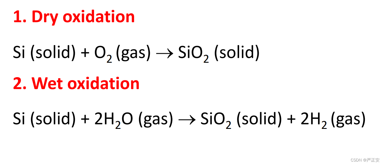
27.wet oxidation and dry oxidation equation
1.什么是直接带隙半导体和间接带隙半导体
导带底和价带顶处以同一K值,称为直接带隙半导体
导带底和价带顶不处在同一K值,称为间接带隙半导体
2.扩散和漂移的公式
3.三五族半导体的性质
1.high mobility
2.wide bandgap
3.direct bandgap
4.三五族半导体的应用
light emitters
microwave devices
UV detectors
5.二六族化合物半导体的优缺点
优点 1. direct and wide gap 2.high luminous efficiency
缺点 1.defects 2. unipolar character
6.二维材料的性质
1.Thin
2.Tunable electrical
3. high transmittance
4.high mobility
5.high thermal conductivity
6.high Young's modulus
7.亮场和暗场的对比
Dark field: 1. field is not exposed 2.used for small spaces
light field 1.field is exposed 2.used for small lines
8.正胶和负胶的对比
正胶 1.high resolution 2.acqueous-based solvents 3.less sensitive
负胶 1.more sensitive 2.more tolerant of developing situation 3.more chemical resistance 4.cheap
5.lower resolution 6.organic-based solvents
9.光刻胶的组成
Resin(树脂或者基材)
Photo active compound (光敏化合物)
solvent(溶剂)
10.光刻的十个基本步骤
1.surface preparation
2.photoresist application
3.soft bake
4.align & expose
5.develop
6.hard bake
7.inspection
8.etch
9.resist strip
10.final inspection
11.光源的要求
1. short wavelength 2.high intensity 3.stable
such as high-pressure mercury lamp and excimer laser
12.对准和曝光系统的种类
1.接触式 contact printing
2.渐进式 proximity printing
3.投影式 projection printing
4.步进式 stepper
13.光刻中,对图像质量起关键作用的两个因素是分辨率和焦深
14.分辨率的公式
K 工艺因子 NA 数值孔径
15.数值孔径公式
16.提升分辨率的三种方法
1.增加NA
2.减小波长
3.减小
17.焦深的公式
18.光刻的发展趋势
1.reduce the feature size
2.reduce the wavelength
3.improve the resolution
4.phase-shift mask
19.扩散的定义,两个种类,两个机理
Mass transport by atomic motion
interdiffusion,self-diffusion
vacancy diffusion,interstitial diffusion
20.空穴扩散速率的两个影响因素
number of vancancies
activation energy to change
21.为什么间质扩散比空穴扩散更快
beacuse more small atoms and more interstitial diffusion
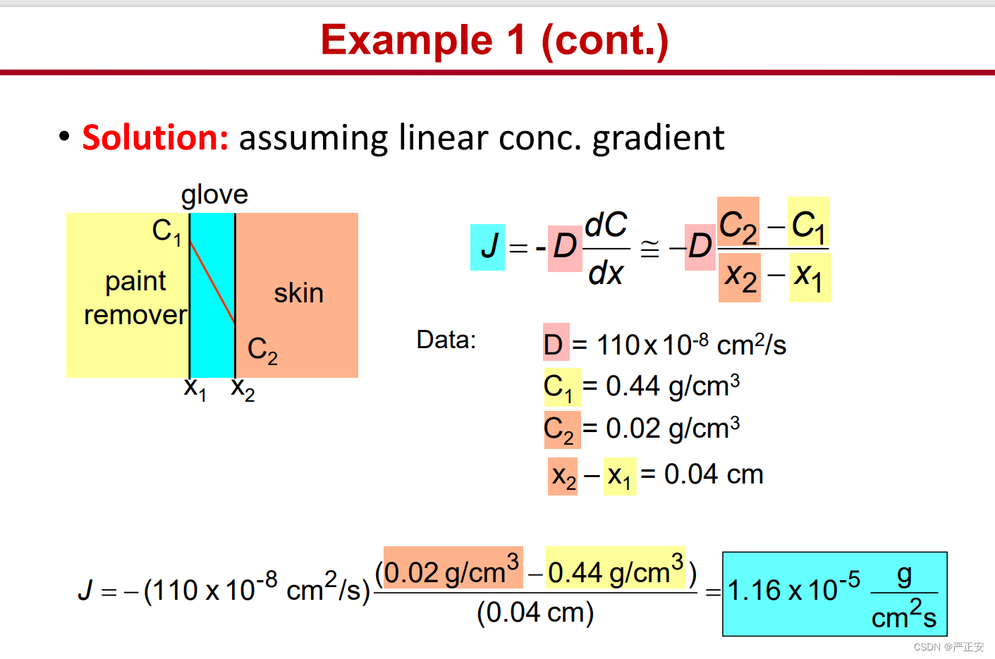
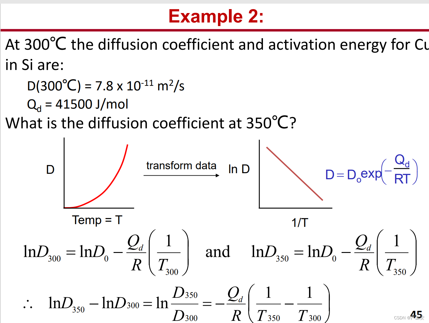
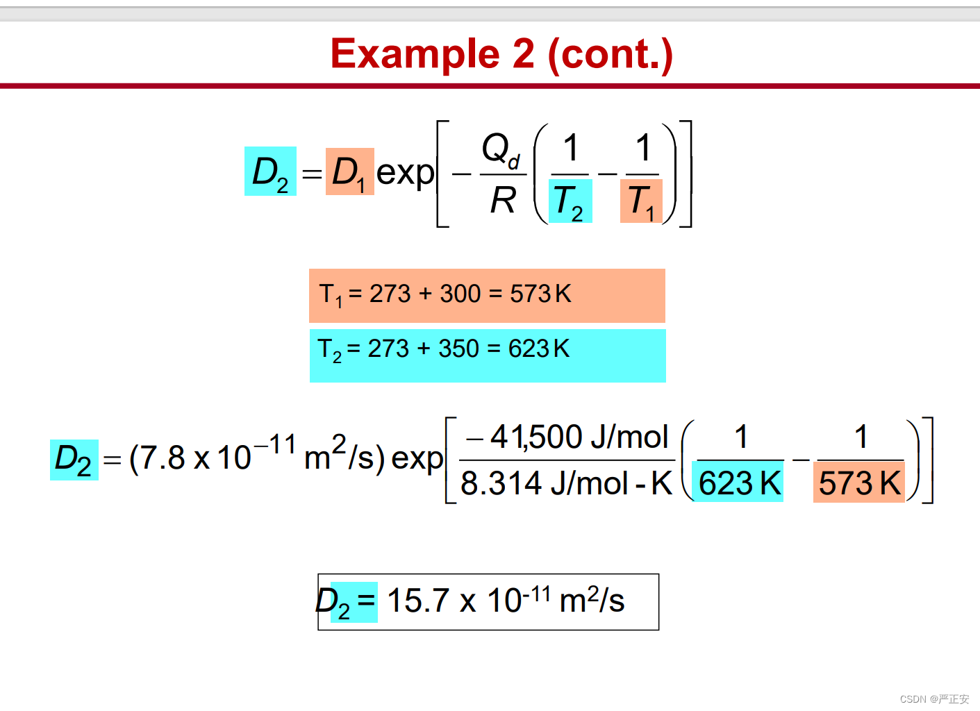
22.菲克第一定律与第二定律的两道练习题
23.杂质扩散的两个步骤以及主要过程
1.predeposition
2.Drive-in
1.predeposition of dopant layer 2.oxidation in window
3.Drive-in 4. Strip and clean
24.热氧化的两个条件
1.high temperature
2. environment
25.二氧化硅的表面层的作用
1.surface passivation(表面钝化)
2.doping Barrier
3.surface dielectric
4.device dielectric
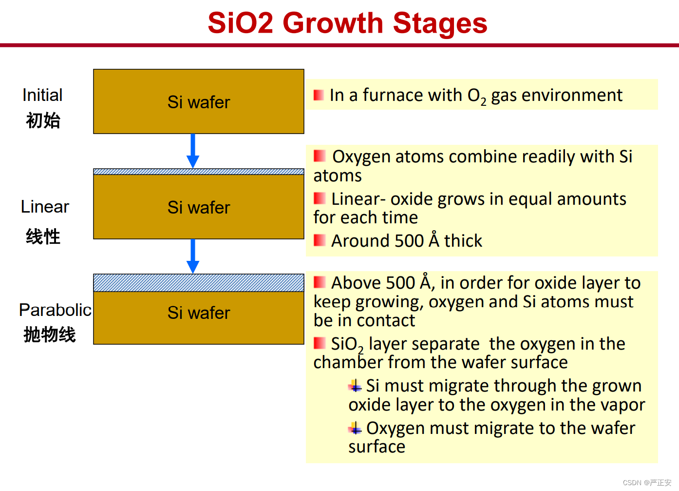
26.二氧化硅的生长过程
27.wet oxidation and dry oxidation equation
28.影响表面生长的两个机理
1.Actual chemical reaction rate between Si and O2
2.diffusion rate
29.如何控制氧化速率
1.wafer orientation
2.waver dopant
3.impurities
4.oxidation of polysilicon layers
30.离子注入的机理
1.隧道效应 Channeling effect
2.阴影效应 shadowing effect
3.stopping mechanism
4.damage production
5.annealing
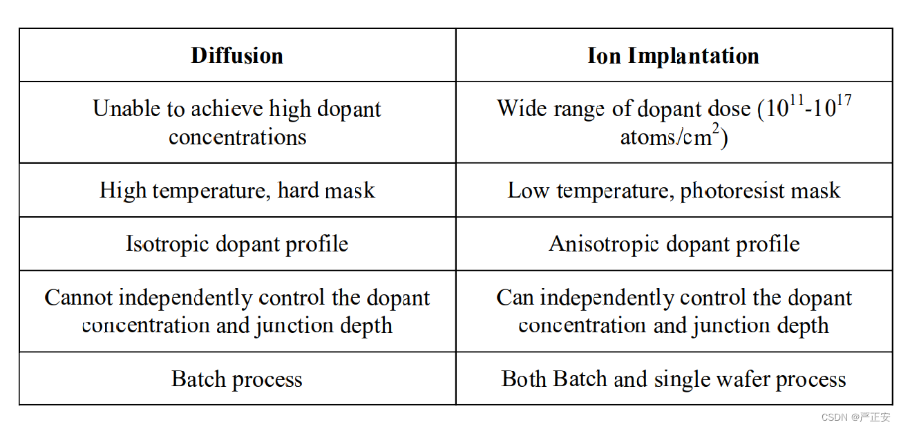
31.离子注入和扩散的对比
32.离子注入的优点
1.precise control of dose and depth profile
2.low-temperature process
3.anisotropic dopant profile
4.less sensitive to surface cleaning procedures
33.两个停止机理
1. nuclear stopping
2. electronic stopping
34.刻蚀的定义
Etch is a main technology for patterning, which is widely used to remove undesired materials from the wafer surface after photolithography.
35.刻蚀的特点
1.chemical,physical or combination of two
2.selective or blanket
36.刻蚀的应用
1.Art work 2.mask making 3.printed circuit Board fabrication 4.silicon solar cells
37.刻蚀的五个术语
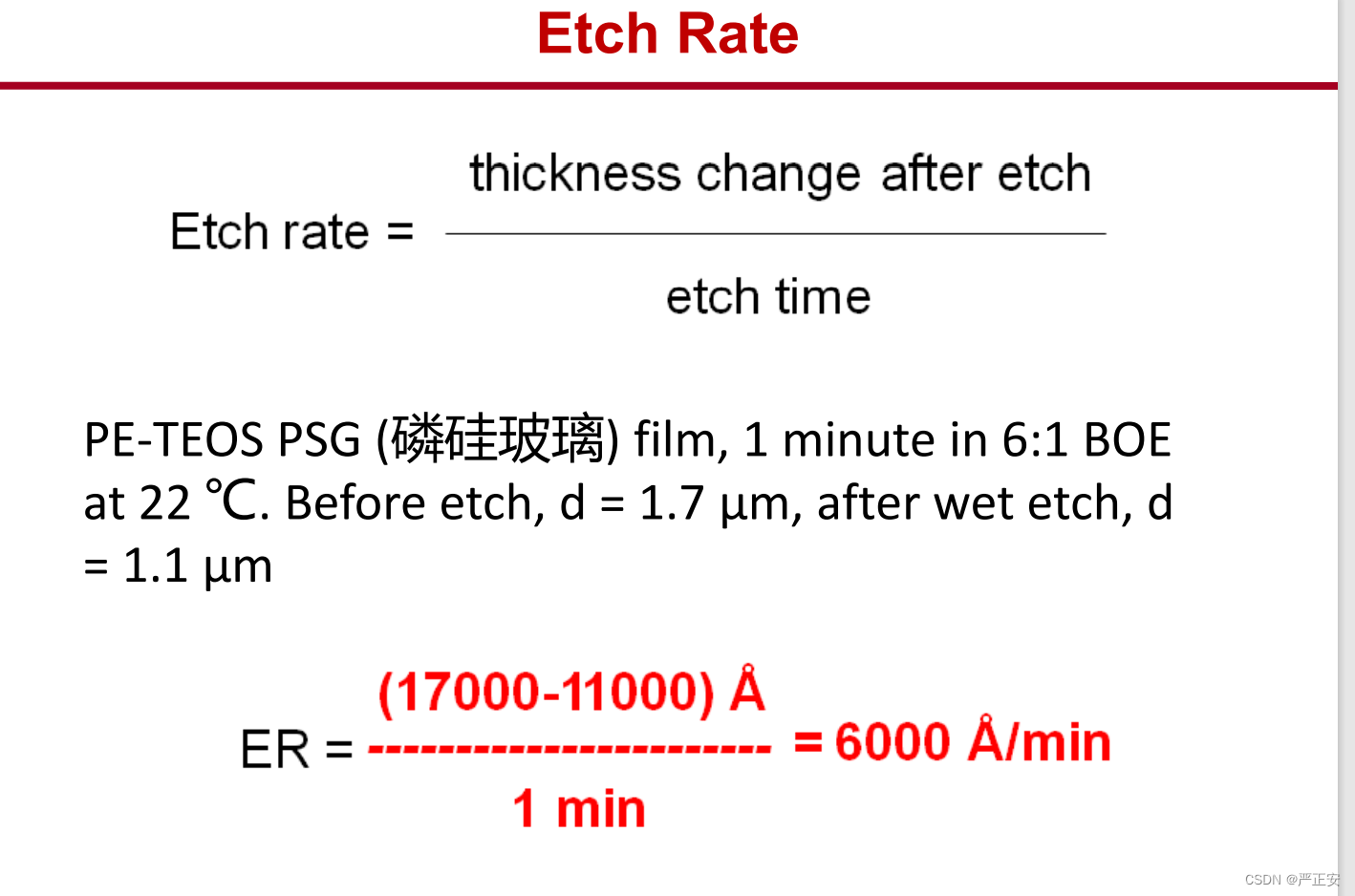
1.刻蚀率 etch rate
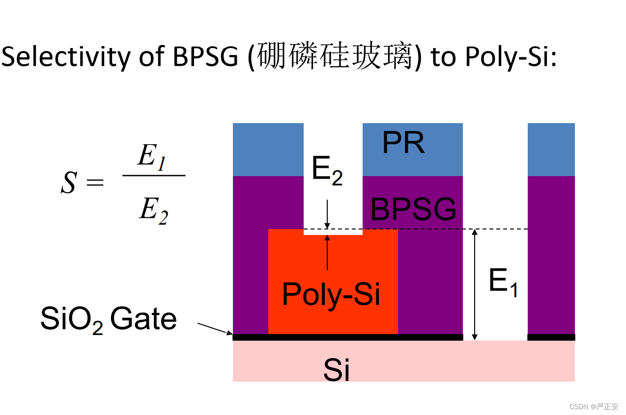
2.挑选性 selectivity: the ratio of each rates of different materials
3. 刻蚀均匀程度 etch uniformity : is a measure of the process repeatability within the wafer (WIW) and wafer to wafer (WTW)
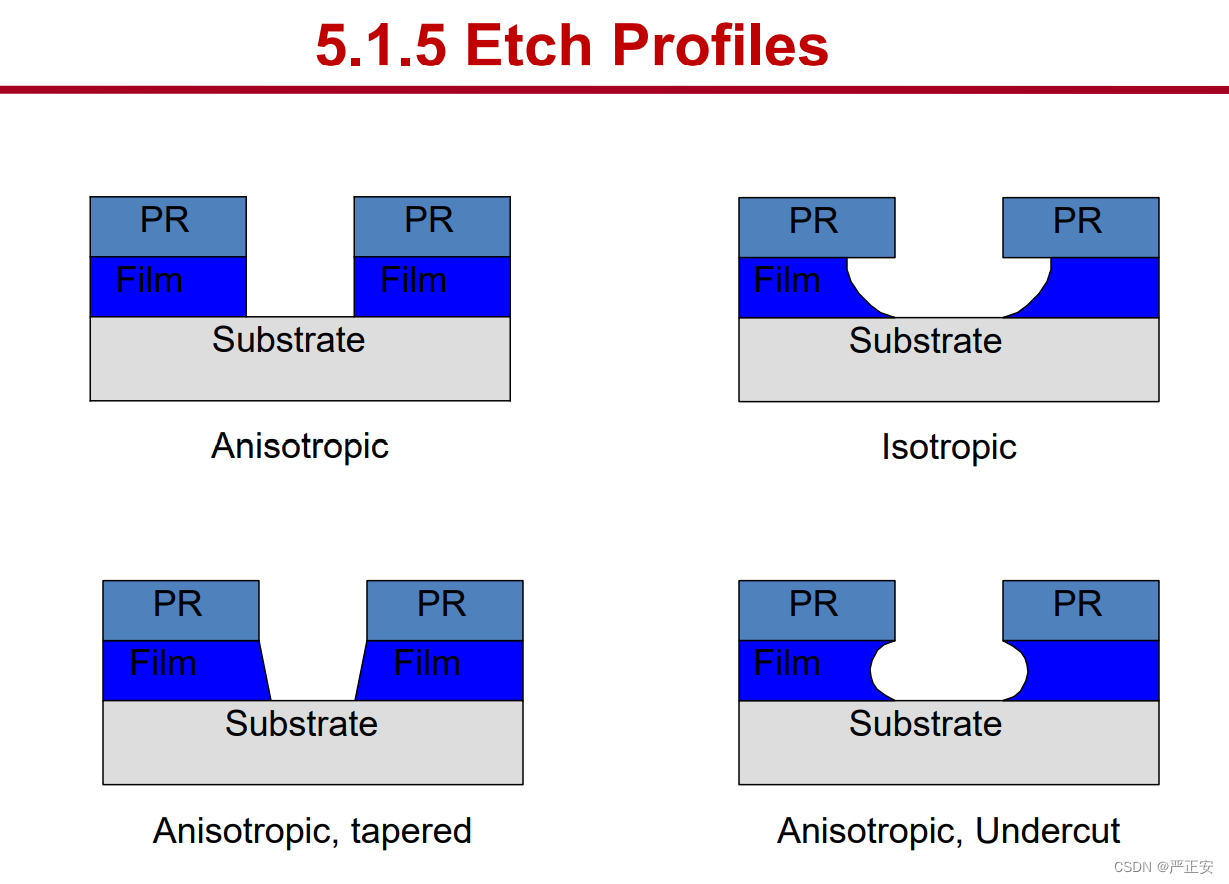
4.各向同性/各向异性的刻蚀 isotropic etch /anisotropuc etch
1. Same etch rate in all directions. (Lateral etch rate is about the same as vertical etch rate)
2. Etch shape does not depend upon the orientation of the mask edge
1. Etch rate depends upon orientation to crystalline planes (Lateral etch rate can be much larger or smaller than vertical etch rate)
2. Orientation of mask edge and the details of the mask pattern determine the final etched shape
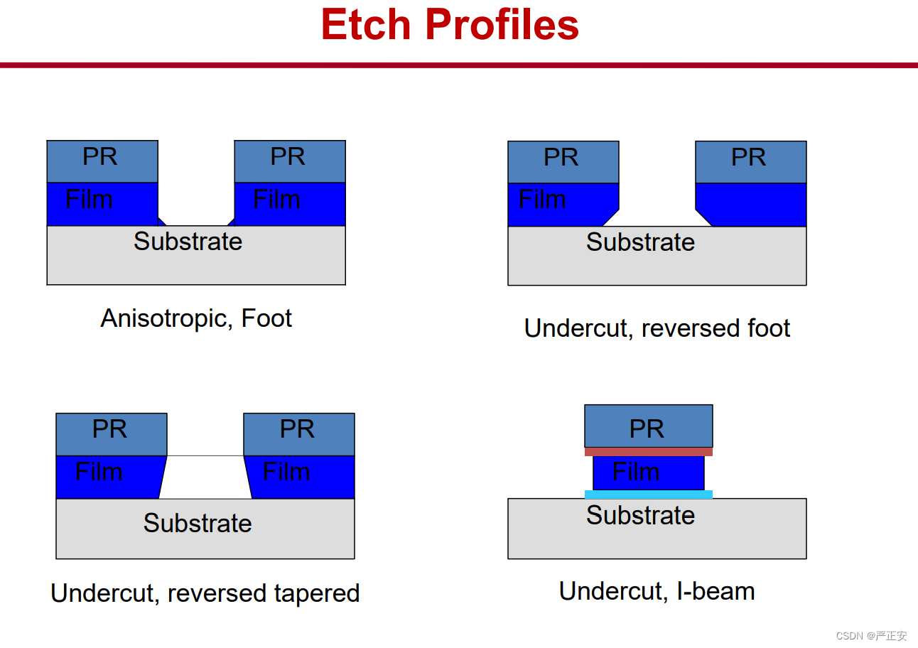
5.刻蚀曲线 etch profile
38.刻蚀的分类
wet etch plasma etch
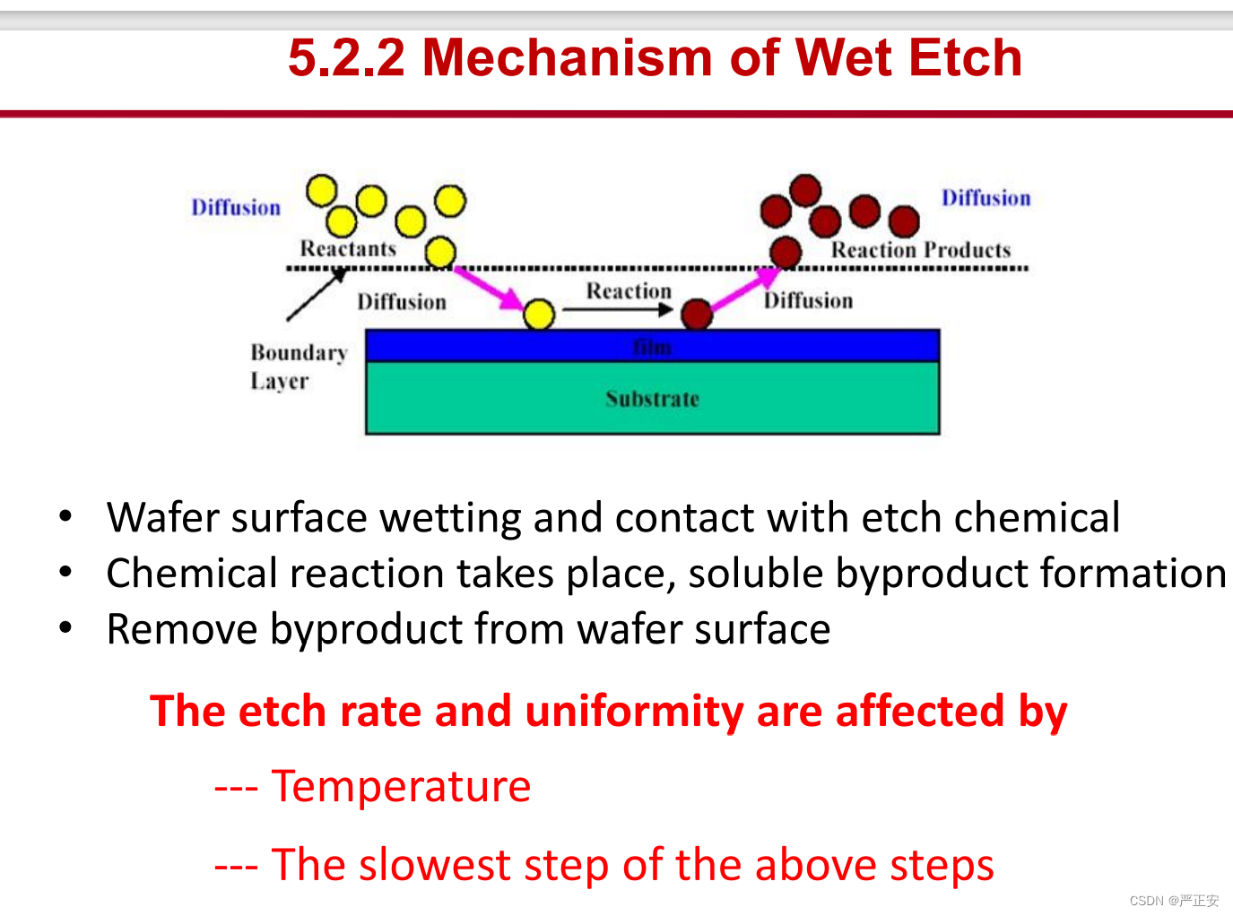
39.湿法刻蚀的定义,主要步骤,副产物
1. use chemical solution to dissolve the materials on the wafer surface
2. Etch & Rinse in an immersion tank
dry in spin-dryer
3. gases,liquids or sulable materials
40.湿法刻蚀的原理
41.湿法刻蚀的特点
1.pure chemical reaction
2.highly selective
3.mainly isotropic etch
4. for use with features >3 微米
5. high throughput
6.low cost equipment
7.hazardous liquid materials
42.湿法刻蚀的优缺点
1.pure chemical reaction
2.highly selective
3. high throughput
4. for use with features >3 微米
5.mainly isotropic etch
6.low cost equipment
7.hazardous liquid materials
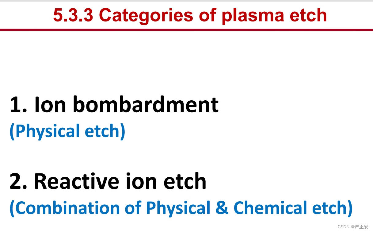
43.干法刻蚀的种类
ion bombardment 离子轰击
reactive ion etch 反应离子刻蚀
44.干法刻蚀的定义
A plasma is an ionized gas with equal numbers of positive and negative charges. Plasma is quasi-neutral.
45.干法刻蚀的特征
1.it contains highly reactive gas species
2.it emits light --- glow
3.it is driven by electric field
4.it is quasi-neutral ni约等于ne
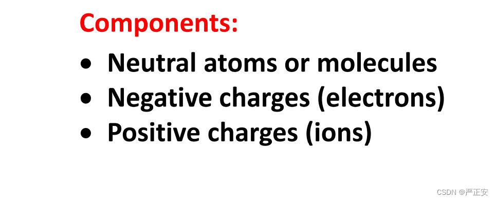
46.等离子体的组成
47.DC power 的特点
require high energy consumption
require conducitive materials for elctrodes
48 RF power的特点
1. in high frequency,electrons will oscillate in the electron gap
2. can work with ielectric materials
3. can operate at lower electorde voltage
4.all commercial plasma processing systems are RF systems
49.等离子体的四个术语
1.Ionization rate
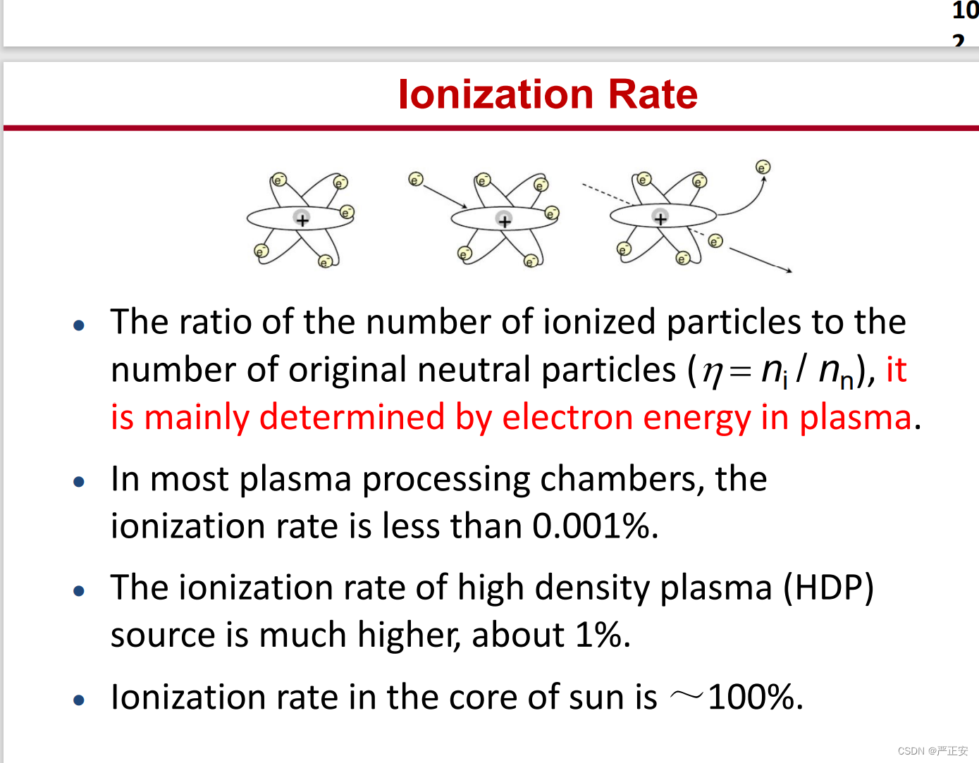
2.mean free path

50.等离子体的种类
51.物理刻蚀的定义,以及特征
physically dislodging material from surface
bomardment with inert ions sych as Ar+
plasma process
anisotropic profile
low selectivity
52.等离子体轰击的应用
1. Help to achieve anisotropic etch profile
2.Argon sputtering
3.help to control film stress in PEVCD process
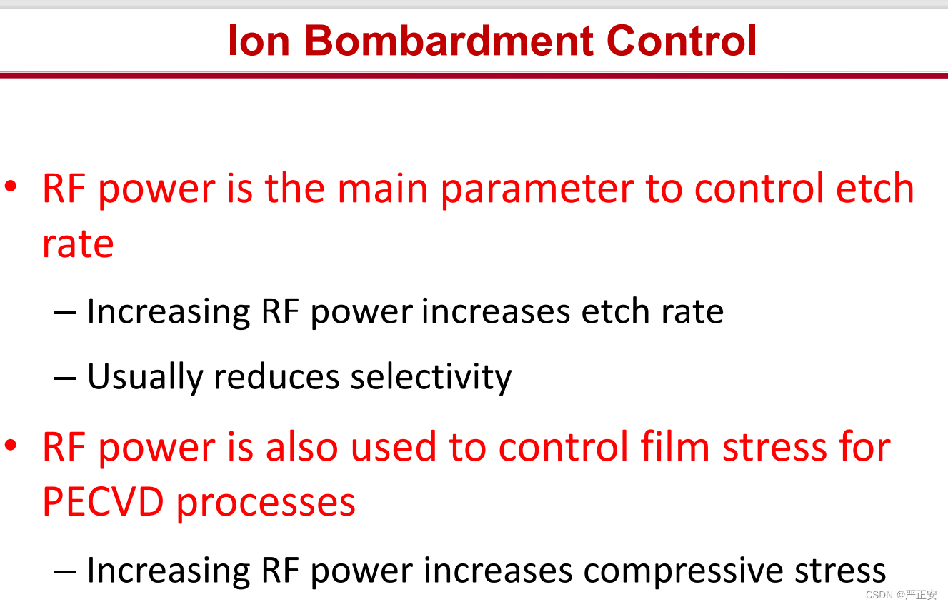
53.如何控制等离子体轰击
54.反应离子刻蚀的两个机理,以及特征
damage mechanism & blocking mechanism
high and controllable rate
anisotropic and contronlable etch profile
Good and controllable selectivity
All patterned etches are RIE processes in 8” fabs
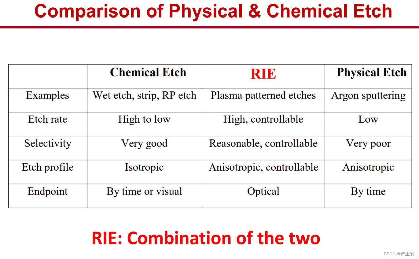
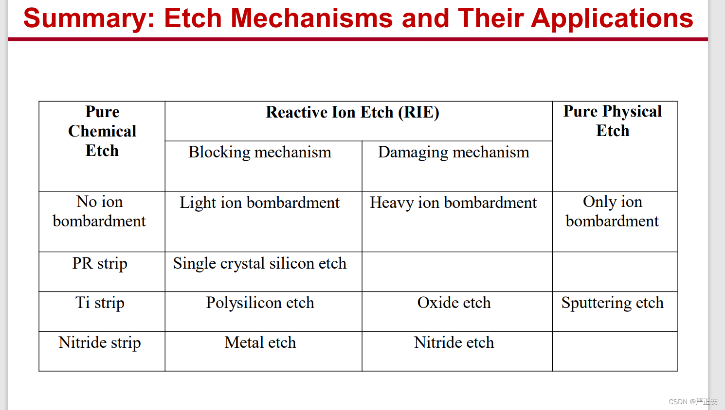
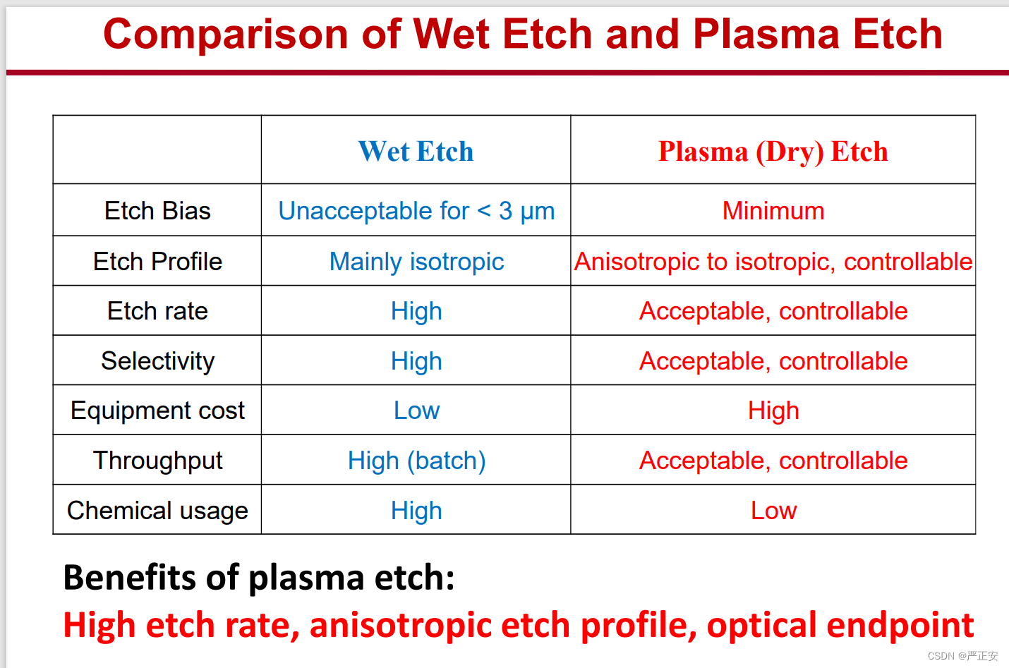
55.三种刻蚀方式的对比
56.刻蚀在CMOS中的应用
Dielectric etch
Single-crystalline silicon etch
Polysilicon etch
Metal etch
Photoresist dry strip
Blanket dry etch
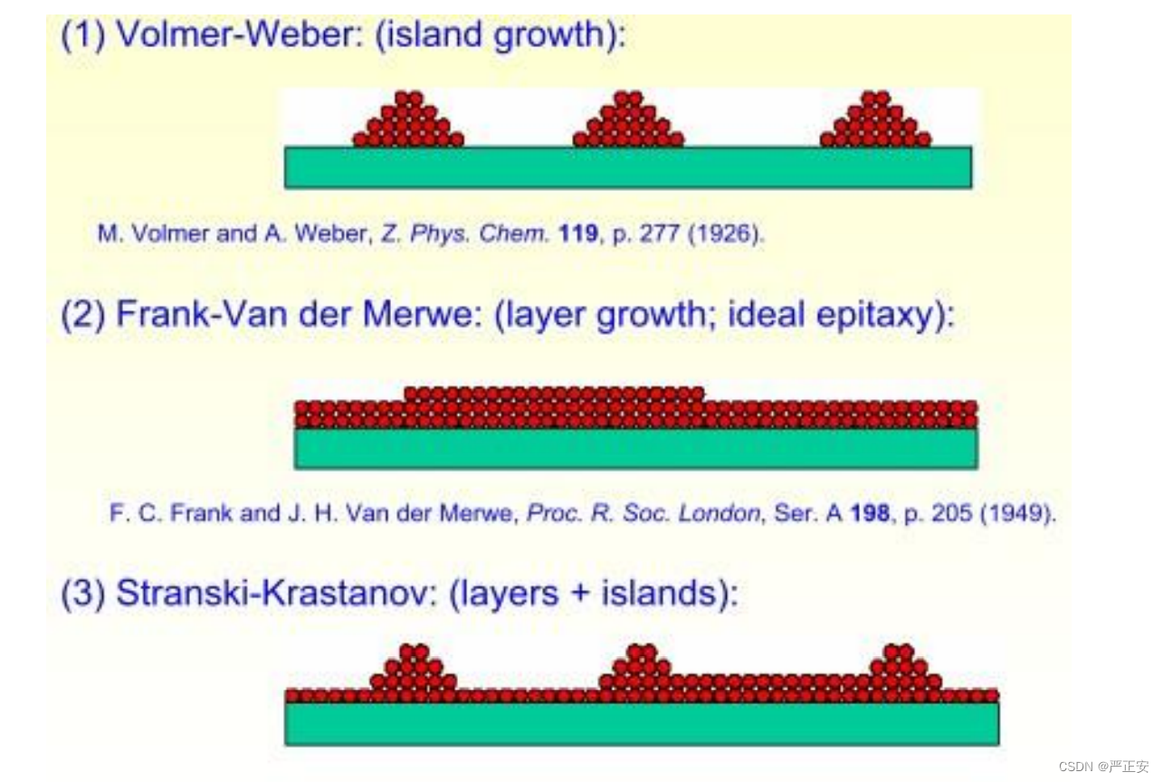
57.薄表面生长的三种方式
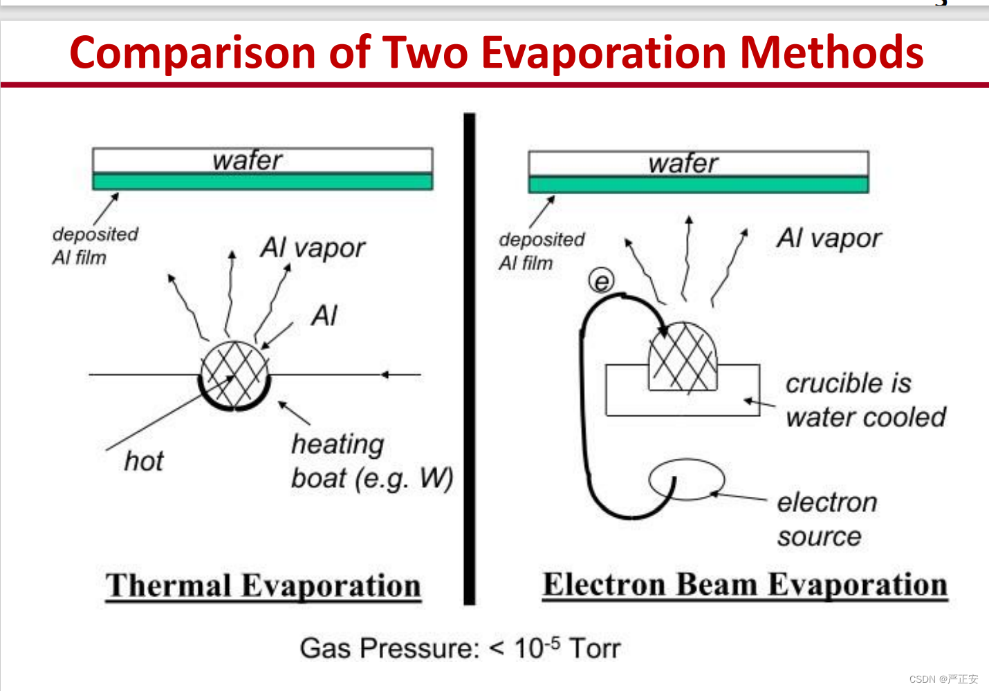
58.物理挥发沉积的两种方式(PVD)
1.Evaporation
2,sputtering
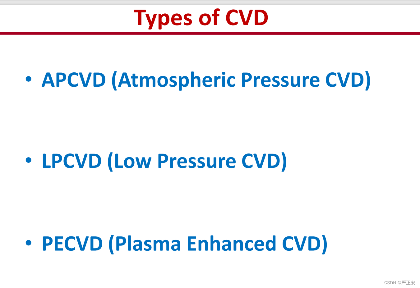
59.化学挥发沉积的两种方式(CVD)
Atmospheric/Low pressure CVD
Plasma enhanced CVD
60.外延沉积的两种方式
MBE
MOCVD
61.两种挥发方式的对比
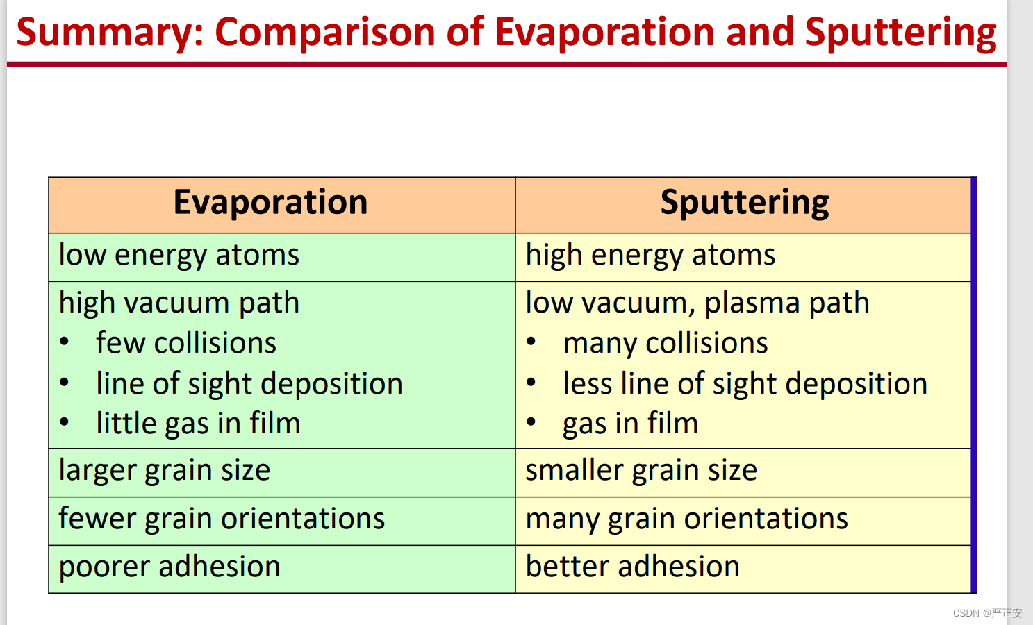
62.sputtering与evaporation的对比
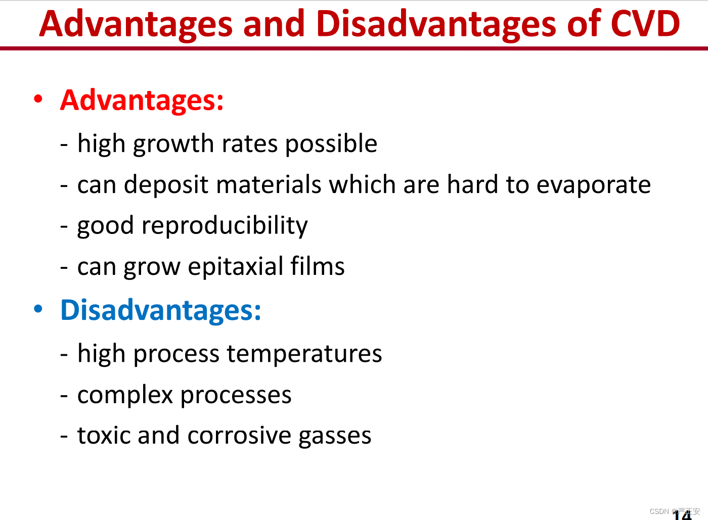
63.CVD的长处与短处
64.薄膜的特征参数
Mechanical properties
Residual stress measurement
Micro/Nanoindentation
Electrical properties
resistance (4 point probe)
capacitance
Optical properties
ellipsometry
Film thickness - Stylus profilometer - ellipsometry
65.微纳加工三种常见工艺
EBL E-beam lithography
FIB Focused ion beam
Nanoimprint NIL
66.EBL的优点与缺点
优点
1.High resolution
2.High flexibility
3.High reliability
4.High reproducibility
缺点
1.Expensive
2.Slow and low throughput
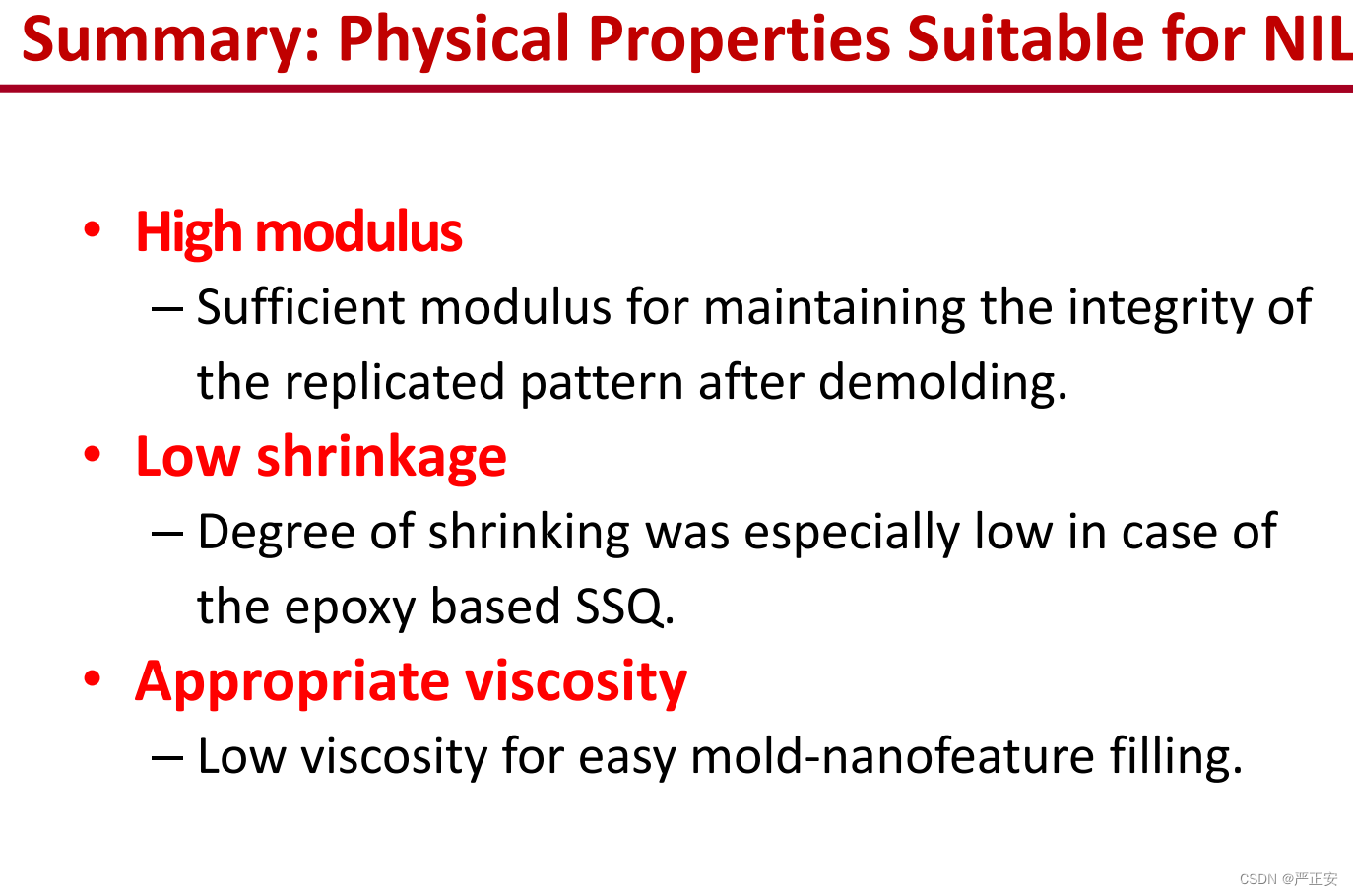
67.NIL的物理性质


 1370
1370


 被折叠的 条评论
为什么被折叠?
被折叠的 条评论
为什么被折叠?
 到【灌水乐园】发言


