


hello,大家好,这里是xddcore。最近开始折腾FPGA,然后今天早上花了一个多小时的时间,搭建了一个D类触发器。为后面要做的BCD Genertor做一些前期工作。(关于 BCD Genertor的设计思路可以看我的这篇博客:https://blog.csdn.net/qq_36229876/article/details/107728996)
前言
什么是D类触发器?
D触发器(data flip-flop或delay flip-flop)由4个与非门组成,其中G1和G2构成基本RS触发器。电平触发的主从触发器工作时,必须在正跳沿前加入输入信号。D触发器在时钟脉冲CP的前沿(正跳变0→1)发生翻转,触发器的次态取决于CP的脉冲上升沿到来之前D端的状态,即次态=D。因此,它具有置0、置1两种功能。由于在CP=1期间电路具有维持阻塞作用,所以在CP=1期间,D端的数据状态变化,不会影响触发器的输出状态。
应用
D触发器应用很广,可用做数字信号的寄存,移位寄存,分频和波形发生器等。在BCD Genertor中,我主要把它当作每次自增1的加法器用。
引脚定义

D, //数据输入
CLK, //时钟(上升沿有效)
SD, //复位(低电平有效),Q置1
RD, //复位(低电平有效),Q置0
Q, //输出端
QN //输出端Q取反
工作原理
如果要用文字来描述工作原理会比较复杂,但是用真值表的话,大家一看就明白了。
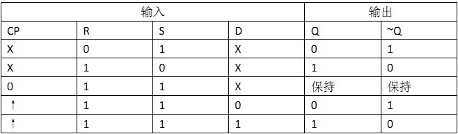
ps:CP=CLK,R=RD,S=SD,~Q=QN
一句话概述D类触发器工作原理:当RD=SD=1时,每当CLK上升沿,便将D上的电平状态赋值给Q,QN等于~Q
再来两句话进行补充说明:
1.当RD=0,SD=1时,D类触发器处于复位低电平保持状态,Q=0,QN=1
1.当RD=1,SD=0时,D类触发器处于复位高电平保持状态,Q=1,QN=0
Verilog程序编写
`timescale 1 ns/ 1 ns //时间单位/时间精度

module data_flip_flop( //定义D类触发器模块
	D, //数据输入
	CLK, //时钟(上升沿有效)
	SD, //复位(低电平有效),Q置1
	RD, //复位(低电平有效),Q置0
	Q, //输出端
	QN //输出端取反
	);

//===========================================================================
// 端口声明与寄存器定义
//===========================================================================
input D; //数据输入
input CLK; //时钟输入(上升沿有效)
input SD; //复位(低电平有效),Q置1
input RD; //复位(低电平有效)
output Q; //输出端
output QN; //输出端取反

reg Q; //1bit的输出Q
reg QN; //1bit的输出QN

//===========================================================================
// 主体逻辑
//===========================================================================
	always @(posedge CLK) //CLK上升沿触发
		begin
			if({RD,SD} == 2'b11) //当RD,SD都为高电平时,每个CLK上升沿,把D的数据取到Q
				begin
					Q <= D; //非阻塞赋值
					QN <= ~D;
				end
			else if({RD,SD} == 2'b01) //当RD=0,SD=1时
				begin
					Q <= 1'b0;
					QN <= 1'b1;
				end
			else if({RD,SD} == 2'b10) //当RD=1,SD=0时
				begin
					Q <= 1'b1;
					QN <= 1'b0;
				end
		end
endmodule //模块结束
TestBench
// Copyright (C) 2017  Intel Corporation. All rights reserved.
// Your use of Intel Corporation's design tools, logic functions
// and other software and tools, and its AMPP partner logic
// functions, and any output files from any of the foregoing
// (including device programming or simulation files), and any
// associated documentation or information are expressly subject
// to the terms and conditions of the Intel Program License
// Subscription Agreement, the Intel Quartus Prime License Agreement,
// the Intel FPGA IP License Agreement, or other applicable license
// agreement, including, without limitation, that your use is for
// the sole purpose of programming logic devices manufactured by
// Intel and sold by Intel or its authorized distributors.  Please
// refer to the applicable agreement for further details.

// *****************************************************************************
// This file contains a Verilog test bench template that is freely editable to
// suit user's needs .Comments are provided in each section to help the user
// fill out necessary details.
// *****************************************************************************
// Generated on "08/04/2020 10:22:36"

// Verilog Test Bench template for design : data_flip_flop
//
// Simulation tool : ModelSim-Altera (Verilog)
//

`timescale 1 ns/ 1 ns
module data_flip_flop_test(); //模块名和vt文件名保持一致
	reg CLK;
	reg D;
	reg RD;
	reg SD;
	// wires
	wire Q;
	wire QN;

	// assign statements (if any)
	data_flip_flop i1 (
	// port map - connection between master ports and signals/registers
		.CLK(CLK),
		.D(D),
		.Q(Q),
		.QN(QN),
		.RD(RD),
		.SD(SD)
	);
	initial //初始化
	begin
		CLK = 1'b1; //时钟线拉高
		D <= 1'b0;  //数据线拉低
		RD <= 1'b1; //ban 0 reset
		SD <= 1'b1; //ban 1 reset
		$display("Running Data flip-flop testbench");
		forever
			begin
				#60 D <= 1'b1;
				#22 D <= 1'b0; //模拟噪声
				#2 D <= 1'b1; //模拟噪声
				#2 D <= 1'b0; //模拟噪声
				#16 D <= 1'b0;
			end
	end
   always #20 CLK <= ~CLK; //生成周期40ns的clk信号

endmodule
RTL仿真结果
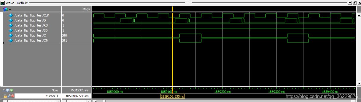
结论
通过上述仿真结果,可以看出,实现了D类触发器的工作效果。本次利用FPGA搭建D类触发器的任务目标实现。


 2097
2097

 被折叠的 条评论
为什么被折叠?
被折叠的 条评论
为什么被折叠?
 到【灌水乐园】发言


