


DSP48E1的整体结构如下:

仿真代码:
// ============================================================
// File Name: tb_dsp_test.v
// VERSION : V1.0
// DATA : 2022/8/27
// Author : FPGA自学笔记分享
// ============================================================
// 功能:fifo测试
// ============================================================
`timescale 1ns/1ps
module tb_dsp_test ;
// ============================================================
// wire reg 信号声明
// ============================================================
reg CLK ='d0 ; // clk
reg RST ='d1 ; // RST
wire [47:0] PCOUT ; // 只能直连PCIN
reg [47:0] PCIN ; // 只能直连PCOUT
reg [3:0] ALUMODE ;
reg [4:0] INMODE ;
reg [6:0] OPMODE ;
reg [29:0] A ;
reg [17:0] B ;
reg [47:0] C ;
reg [24:0] D ;
wire [47:0] P ;
// assign PCIN = 48'd10;
// ============================================================
// main
// ============================================================
always #1 CLK = ~CLK;
initial begin
RST = 1'b1;
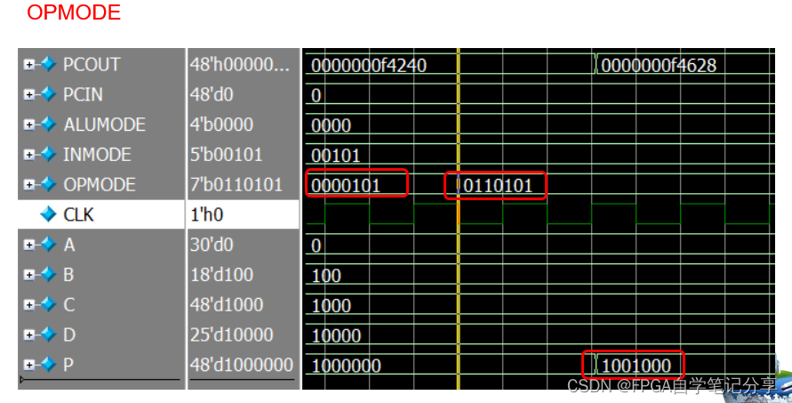
INMODE = 5'b00101 ; //(D+A1)*B2
OPMODE = 7'b0000101 ; ///C+ M
ALUMODE= 4'b0000;
PCIN = 48'd0;
#2000;
RST = 1'b0;
#200;
// PCIN = 48'd10;
OPMODE = 7'b0110101 ; /// M
end
// ============================================================
// data_in
// ============================================================
always @(posedge CLK)
if(RST)
begin
A <= 30'd0;
B <= 18'd100;
C <= 48'd1000;
D <= 25'd10000;
end
else
begin
A <= A ; //+ 'd1;
B <= B ; //+ 'd1;
C <= C ; //+ 'd1;
D <= D ; //+ 'd1;
end
// always @(posedge CLK)
// if(A[4])
// OPMODE = 7'b0110101 ; /// C M
// else
// OPMODE = 7'b0000101 ; /// 0 M
// ============================================================
// DSP48E1
// ============================================================
DSP48E1 #(
// Feature Control Attributes: Data Path Selection
.A_INPUT ("DIRECT" ), // Selects A input source, "DIRECT" (A port) or "CASCADE" (ACIN port)
.B_INPUT ("DIRECT" ), // Selects B input source, "DIRECT" (B port) or "CASCADE" (BCIN port)
.USE_DPORT ("TRUE" ), // Select D port usage (TRUE or FALSE)
.USE_MULT ("MULTIPLY" ), // Select multiplier usage ("MULTIPLY", "DYNAMIC", or "NONE")
.USE_SIMD ("ONE48" ), // SIMD selection ("ONE48", "TWO24", "FOUR12")
// Pattern Detector Attributes: Pattern Detection Configuration
.AUTORESET_PATDET ("NO_RESET" ), // "NO_RESET", "RESET_MATCH", "RESET_NOT_MATCH"
.MASK (48'h3fffffffffff ), // 48-bit mask value for pattern detect (1=ignore)
.PATTERN (48'h000000000000 ), // 48-bit pattern match for pattern detect
.SEL_MASK ("MASK" ), // "C", "MASK", "ROUNDING_MODE1", "ROUNDING_MODE2"
.SEL_PATTERN ("PATTERN" ), // Select pattern value ("PATTERN" or "C")
.USE_PATTERN_DETECT ("NO_PATDET" ), // Enable pattern detect ("PATDET" or "NO_PATDET")
// Register Control Attributes: Pipeline Register Configuration
.ACASCREG (1 ), // Number of pipeline stages between A/ACIN and ACOUT (0, 1 or 2)
.ADREG (1 ), // Number of pipeline stages for pre-adder (0 or 1)
.ALUMODEREG (1 ), // Number of pipeline stages for ALUMODE (0 or 1)
.AREG (1 ), // Number of pipeline stages for A (0, 1 or 2)
.BCASCREG (1 ), // Number of pipeline stages between B/BCIN and BCOUT (0, 1 or 2)
.BREG (2 ), // Number of pipeline stages for B (0, 1 or 2)
.CARRYINREG (1 ), // Number of pipeline stages for CARRYIN (0 or 1)
.CARRYINSELREG (1 ), // Number of pipeline stages for CARRYINSEL (0 or 1)
.CREG (1 ), // Number of pipeline stages for C (0 or 1)
.DREG (1 ), // Number of pipeline stages for D (0 or 1)
.INMODEREG (1 ), // Number of pipeline stages for INMODE (0 or 1)
.MREG (1 ), // Number of multiplier pipeline stages (0 or 1)
.OPMODEREG (1 ), // Number of pipeline stages for OPMODE (0 or 1)
.PREG (1 ) // Number of pipeline stages for P (0 or 1)
)
DSP48E1_inst (
// Cascade: 30-bit (each) output: Cascade Ports
.ACOUT ( ), // 30-bit output: A port cascade output
.BCOUT ( ), // 18-bit output: B port cascade output
.CARRYCASCOUT ( ), // 1-bit output: Cascade carry output
.MULTSIGNOUT ( ), // 1-bit output: Multiplier sign cascade output
.PCOUT (PCOUT ), // 48-bit output: Cascade output
// Control: 1-bit (each) output: Control Inputs/Status Bits
.OVERFLOW ( ), // 1-bit output: Overflow in add/acc output
.PATTERNBDETECT ( ), // 1-bit output: Pattern bar detect output
.PATTERNDETECT ( ), // 1-bit output: Pattern detect output
.UNDERFLOW ( ), // 1-bit output: Underflow in add/acc output
// Data: 4-bit (each) output: Data Ports
.CARRYOUT ( ), // 4-bit output: Carry output
.P (P ), // 48-bit output: Primary data output
// Cascade: 30-bit (each) input: Cascade Ports
.ACIN (30'd0 ), // 30-bit input: A cascade data input
.BCIN (18'd0 ), // 18-bit input: B cascade input
.CARRYCASCIN (1'b1 ), // 1-bit input: Cascade carry input
.MULTSIGNIN (1'b1 ), // 1-bit input: Multiplier sign input
.PCIN (PCIN ), // 48-bit input: P cascade input
// Control: 4-bit (each) input: Control Inputs/Status Bits
.ALUMODE (ALUMODE ), // 4-bit input: ALU control input
.CARRYINSEL (3'd0 ), // 3-bit input: Carry select input
.CLK (CLK ), // 1-bit input: Clock input
.INMODE (INMODE ), // 5-bit input: INMODE control input
.OPMODE (OPMODE ), // 7-bit input: Operation mode input
// Data: 30-bit (each) input: Data Ports
.A (A ), // 30-bit input: A data input
.B (B ), // 18-bit input: B data input
.C (C ), // 48-bit input: C data input
.CARRYIN (1'b0 ), // 1-bit input: Carry input signal
.D (D ), // 25-bit input: D data input
// Reset/Clock Enable: 1-bit (each) input: Reset/Clock Enable Inputs
.CEA1 (1'b1 ), // 1-bit input: Clock enable input for 1st stage AREG
.CEA2 (1'b1 ), // 1-bit input: Clock enable input for 2nd stage AREG
.CEAD (1'b1 ), // 1-bit input: Clock enable input for ADREG
.CEALUMODE (1'b1 ), // 1-bit input: Clock enable input for ALUMODE
.CEB1 (1'b1 ), // 1-bit input: Clock enable input for 1st stage BREG
.CEB2 (1'b1 ), // 1-bit input: Clock enable input for 2nd stage BREG
.CEC (1'b1 ), // 1-bit input: Clock enable input for CREG
.CECARRYIN (1'b1 ), // 1-bit input: Clock enable input for CARRYINREG
.CECTRL (1'b1 ), // 1-bit input: Clock enable input for OPMODEREG and CARRYINSELREG
.CED (1'b1 ), // 1-bit input: Clock enable input for DREG
.CEINMODE (1'b1 ), // 1-bit input: Clock enable input for INMODEREG
.CEM (1'b1 ), // 1-bit input: Clock enable input for MREG
.CEP (1'b1 ), // 1-bit input: Clock enable input for PREG
.RSTA (RST ), // 1-bit input: Reset input for AREG
.RSTALLCARRYIN (RST ), // 1-bit input: Reset input for CARRYINREG
.RSTALUMODE (RST ), // 1-bit input: Reset input for ALUMODEREG
.RSTB (RST ), // 1-bit input: Reset input for BREG
.RSTC (RST ), // 1-bit input: Reset input for CREG
.RSTCTRL (RST ), // 1-bit input: Reset input for OPMODEREG and CARRYINSELREG
.RSTD (RST ), // 1-bit input: Reset input for DREG and ADREG
.RSTINMODE (RST ), // 1-bit input: Reset input for INMODEREG
.RSTM (RST ), // 1-bit input: Reset input for MREG
.RSTP (RST ) // 1-bit input: Reset input for PREG
);
// End of DSP48E1_inst instantiation
endmodule仿真直接调用dsp48e1的源语,通过修改inmode,altmode,opmode来验证dap48e1的功能:
inmode使用00101,让A、B、D三个端口对齐输入,C延后两个clk;
opmode[3:0]使用0101,使用M作为X,Y的数据;
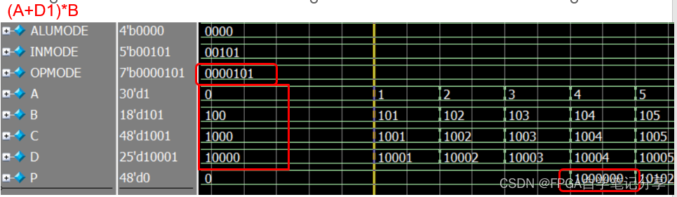
1、(A+D1)*B
2、(A+D1)*B+C

3、(A+D1)*B+Pcin

4、OPMODE
inmode使用00101,让A、B、D三个端口对齐输入,C延后两个clk
opmode[3:0]使用0101,使用M作为X,Y的数据;
这种情况下:
1、 A、B、D三个端口对齐在同一时刻输入;
2、P在数据 A、B、D输入后的第四个clk输出;
3、C数据在数据 A、B、D输入的第二个clk输入;
4、Pcin级联时数据要在数据 A、B、D输入的第三个clk输入;
5、 OPMODE,ALUMODE在数据 A、B、D输入的第二个clk输入;
详细的视频讲解可见B站视频:
【FPGA的底层资源之DSP48E1仿真】 https://www.bilibili.com/video/BV19V4y1W7hj/?share_source=copy_web&vd_source=9736f43bc2eebc284f4fbbe5805247a7


 1万+
1万+


 被折叠的 条评论
为什么被折叠?
被折叠的 条评论
为什么被折叠?
 到【灌水乐园】发言


