


2023.3.8&3.9
祝自己节日快乐呀!上午拍花花去了,下午陪npy听了招聘会,下午五点才开始学习,嘿嘿,也算小放假一下!


一、绘制(overlay)图像(y=0.241um处电场强度随电压变化曲线)
1.1代码
method newton trap maxtrap=10 climit=1e-4
solve vcathode=1
save outf=pin_p1.str
solve vcathode=5
save outf=pin_p5.str
solve vcathode=15
save outf=pin_1p5.str
solve vcathode=30
save outf=pin_3p0.str
solve vcathode=42.5
save outf=pin_4p25.str
solve vcathode=60
save outf=pin_6p0.str
# EL Electric Field at 1V, 5V and 15.0V 30V, 42.5V and 60.0V
tonyplot pin_p1.str
extract init infile="pin_p1.str"
extract name="EleF" curve(depth,impurity="Electric Field" material="All" \
        y.val=0.241) outfile="pin_p1.dat"

extract init infile="pin_p5.str"
extract name="EleF" curve(depth,impurity="Electric Field" material="All" \
        y.val=0.241) outfile="pin_p5.dat"

extract init infile="pin_1p5.str"
extract name="EleF" curve(depth,impurity="Electric Field" material="All" \
        y.val=0.241) outfile="pin_1p5.dat"

extract init infile="pin_3p0.str"
extract name="EleF" curve(depth,impurity="Electric Field" material="All" \
        y.val=0.241) outfile="pin_3p0.dat"

extract init infile="pin_4p25.str"
extract name="EleF" curve(depth,impurity="Electric Field" material="All" \
        y.val=0.241) outfile="pin_4p25.dat"

extract init infile="pin_6p0.str"
extract name="EleF" curve(depth,impurity="Electric Field" material="All" \
        y.val=0.241) outfile="pin_6p0.dat"

tonyplot pin_p1.dat
tonyplot pin_p5.dat
tonyplot pin_1p5.dat
tonyplot pin_3p0.dat
tonyplot pin_4p25.dat
tonyplot pin_6p0.dat
tonyplot -overlay pin_p1.dat pin_p5.dat pin_1p5.dat  pin_3p0.dat pin_4p25.dat pin_6p0.dat
1.2说明:
分别令Vcathode=1、5、15、30、42.5、60V,保存求解(solve)后的器件结构
然后分别从六个器件结构中提取Electric Field-Width曲线并绘制在同一窗口
注意,上述代码,若将curve()里的depth改成width,则会报错,说语法不对,impurity没有ElectricField
TPCS
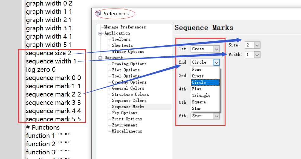
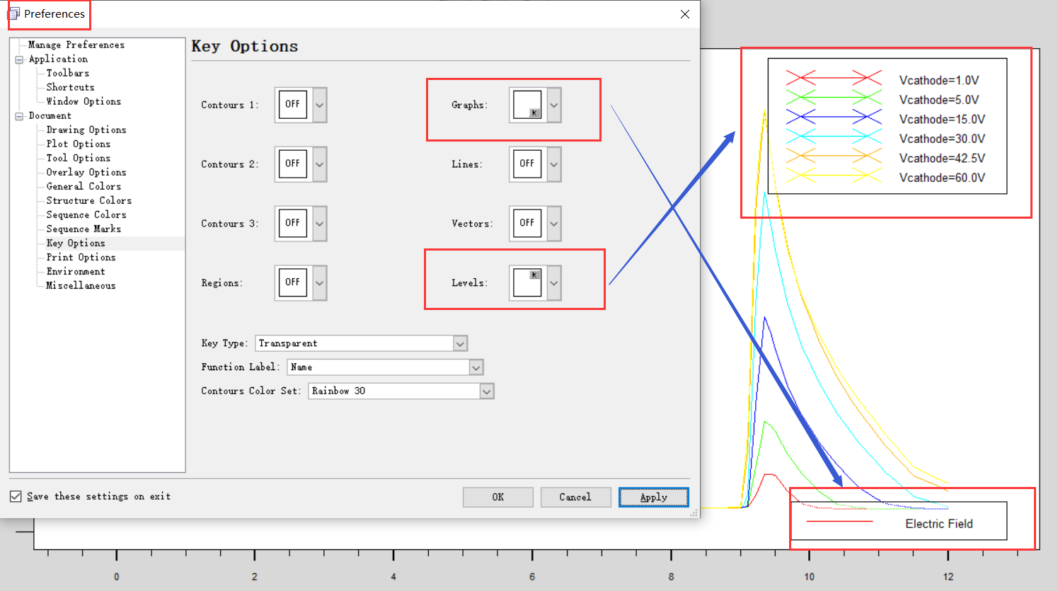
key coutours:

sequence
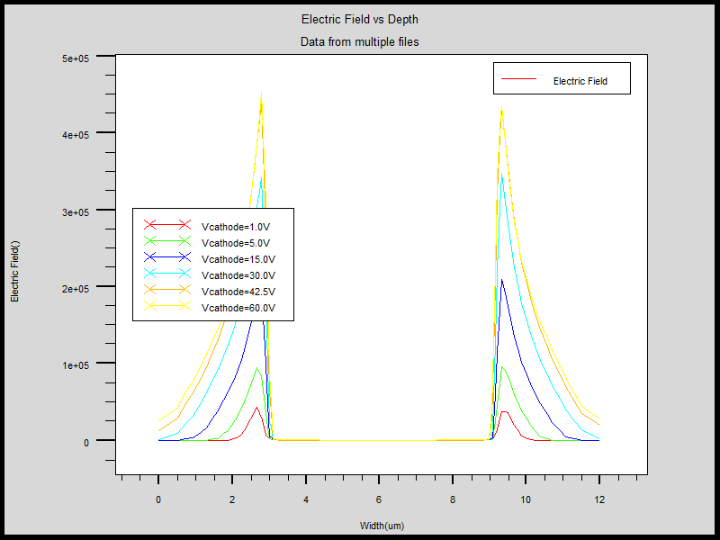
42.5V和60V曲线重合,说明器件已击穿
从led01学到的:
保存不同状态的结构,从中提取多条曲线并绘制在一张图上,直观明了
TPCS语言和实际的tonyplot窗口相对应
写代码的时候可以注明模块和前边的说明,可以增强可读性。
二、LED第二个例子学习
2.1 代码:
# (c) Silvaco Inc., 2013
go atlas
# GaN LED Opto Device Simulation
#
# UltraViolet Multi-quantum well LED
# APL Vol.73 No.12. 21 Sep.(1998) pp.1688-1690
#
# Parameter used for this UV MQW LED
#############################################################################
# Epilayer # Material # Type # Thickness # Doping # Mobility #
# # # p or n # [nm] # [cm-3] # [cm2/V-s] #
#############################################################################
# p-Contact # GaN # p # 100 # 1e20 # 10 #
# p-Emitter # Al0.10GaN # p # 200 # 1e20 # 10 #
# p-Emitter # Al0.20GaN # p # 100 # 1e20 # 10 #
# 4MQW # GaN # - # 3 # - # 200 #
# 3Barrier # Al0.2GaN # - # 7 # - # 100 #
# n-Emitter # Al0.2GaN # n # 100 # 2e18 # 100 #
# n-Contact # GaN # n # 300 # 2e18 # 100 #
#############################################################################
# 1 Dimensional Structure
# for A Cylindrical 120 diameter(3.14*60*60=1.13e4)
mesh width=1.13e4
#
x.mesh loc=0.0 spac=0.5
x.mesh loc=1.0 spac=0.5
#
y.mesh loc=0.0 spac=0.05
y.mesh loc=0.1 spac=0.001
y.mesh loc=0.2 spac=0.025
y.mesh loc=0.3 spac=0.001
y.mesh loc=0.35 spac=0.01
y.mesh loc=0.4 spac=0.0005
y.mesh loc=0.433 spac=0.0005
y.mesh loc=0.483 spac=0.001
y.mesh loc=0.533 spac=0.001
y.mesh loc=2.033 spac=0.10
y.mesh loc=3.533 spac=0.01
#
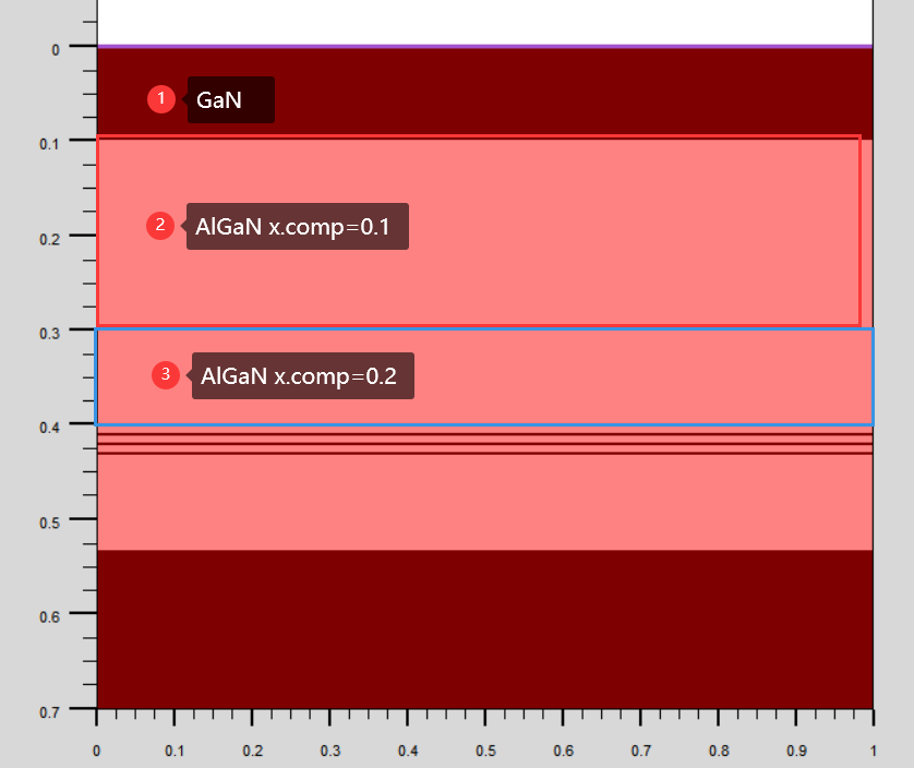
region number=1 y.max=0.1 material=GaN
region number=2 y.min=0.1 y.max=0.3 material=AlGaN x.comp=0.1
region number=3 y.min=0.3 y.max=0.4 material=AlGaN x.comp=0.2
#
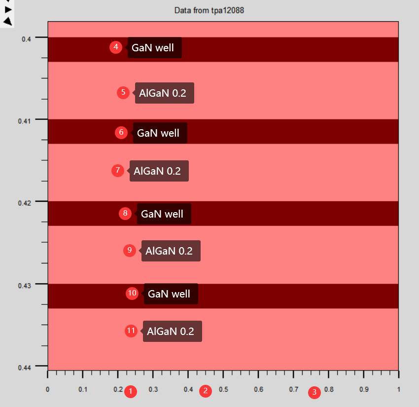
# 4 MQW
#
region number=4 y.min=0.4 y.max=0.403 material=GaN name=well led qwell
region number=5 y.min=0.403 y.max=0.410 material=AlGaN x.comp=0.2
region number=6 y.min=0.410 y.max=0.413 material=GaN name=well led qwell
region number=7 y.min=0.413 y.max=0.420 material=AlGaN x.comp=0.2
region number=8 y.min=0.420 y.max=0.423 material=GaN name=well led qwell
region number=9 y.min=0.423 y.max=0.430 material=AlGaN x.comp=0.2
region number=10 y.min=0.430 y.max=0.433 material=GaN name=well led qwell
region number=11 y.min=0.433 y.max=0.533 material=AlGaN x.comp=0.2
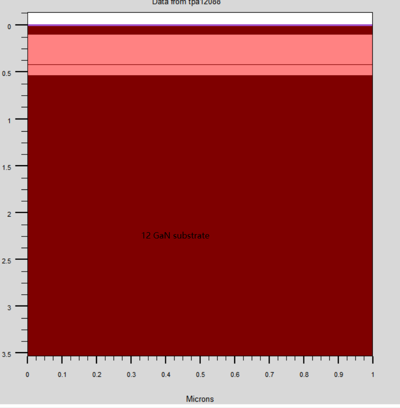
region number=12 y.min=0.533 y.max=3.533 material=GaN substrate
#
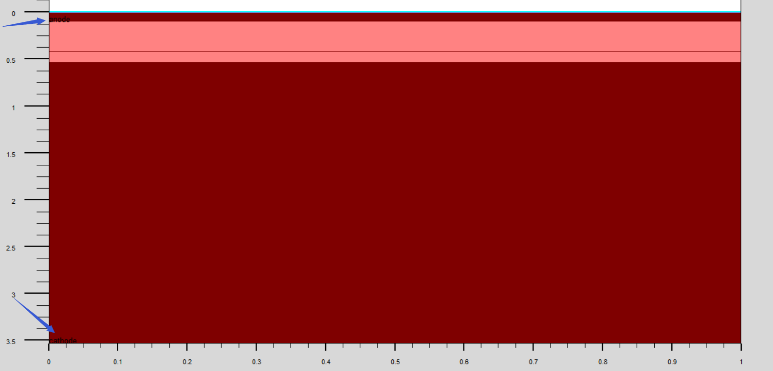
electrode name=anode top
electrode name=cathode bottom
#
doping region=1 uniform p.type conc=1e20
doping region=2 uniform p.type conc=1e20
doping region=3 uniform p.type conc=1e20
# doping 4~10 intrinsic
doping region=11 uniform n.type conc=2e18
doping region=12 uniform n.type conc=2e18
#
models polarization calc.strain polar.scale=0.15
material material=GaN taun0=1e-9 taup0=1e-9 copt=1.1e-8 \
augn=1.0e-34 augp=1.0e-34
material material=AlGaN taun0=1e-9 taup0=1e-9 copt=1.1e-8 \
augn=1.0e-34 augp=1.0e-34
material material=InGaN taun0=1e-9 taup0=1e-9 copt=1.1e-8 \
augn=1.0e-34 augp=1.0e-34
#
material well.gamma0=10e-3
#
material edb=0.080 eab=0.101
#
models k.p fermi incomplete consrh auger optr print
models name=well k.p chuang spontaneous lorentz
#
mobility material=GaN mun0=300 mup0=10
mobility material=AlGaN mun0=250 mup0=5
#
output con.band val.band band.param charge polar.charge e.mobility h.mobility \
u.srh u.radiative u.auger permi
#
solve init
#
method climit=1e-4 maxtrap=10
#block nblockit=50
#
solve prev
#
save outf=ledex02_1.str
#
probe name="Radiative" integrate radiative rname=well
probe name="Recombination" integrate recombination
#
log outf=ledex02.log
solve vstep=0.1 vfinal=2.5 name=anode
save outf=ledex02_2p5.str
save spectrum=ledex02_2p5.spc lmin=0.33 lmax=0.38 nsamp=100
solve vstep=0.1 vfinal=3.0 name=anode
save outf=ledex02_3p0.str
save spectrum=ledex02_3p0.spc lmin=0.33 lmax=0.38 nsamp=100
solve vstep=0.1 vfinal=3.5 name=anode
save outf=ledex02_3p5.str
save spectrum=ledex02_3p5.spc lmin=0.33 lmax=0.38 nsamp=100
solve vstep=0.1 vfinal=4.0 name=anode
save outf=ledex02_4p0.str
save spectrum=ledex02_4p0.spc lmin=0.33 lmax=0.38 nsamp=100
solve vstep=0.1 vfinal=5.0 name=anode
save outf=ledex02_5p0.str
solve vstep=0.1 vfinal=6.0 name=anode
save outf=ledex02_6p0.str
#
# V-I Curve
tonyplot ledex02.log -set ledex02_0.set
# I-L Curve
tonyplot ledex02.log -set ledex02_1.set
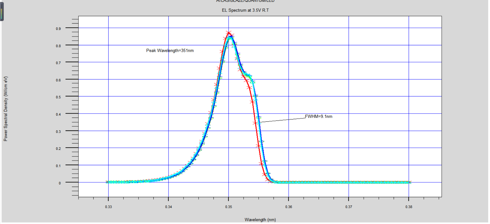
# EL Spectrum
tonyplot ledex02_3p5.spc -set ledex02_2.set
# Extract the Electron And hole Conc.
extract init infile="ledex02_3p5.str"
extract name="Electron" curve(depth,impurity="Electron Conc" material="All" \
x.val=0.5) outfile="ledex02_3p5_Electron.dat"
extract name="Electron" curve(depth,impurity="Hole Conc" material="All" \
x.val=0.5) outfile="ledex02_3p5_Hole.dat"
extract init infile="ledex02_4p0.str"
extract name="Electron" curve(depth,impurity="Electron Conc" material="All" \
x.val=0.5) outfile="ledex02_4p0_Electron.dat"
extract name="Electron" curve(depth,impurity="Hole Conc" material="All" \
x.val=0.5) outfile="ledex02_4p0_Hole.dat"
extract init infile="ledex02_5p0.str"
extract name="Electron" curve(depth,impurity="Electron Conc" material="All" \
x.val=0.5) outfile="ledex02_5p0_Electron.dat"
extract name="Electron" curve(depth,impurity="Hole Conc" material="All" \
x.val=0.5) outfile="ledex02_5p0_Hole.dat"
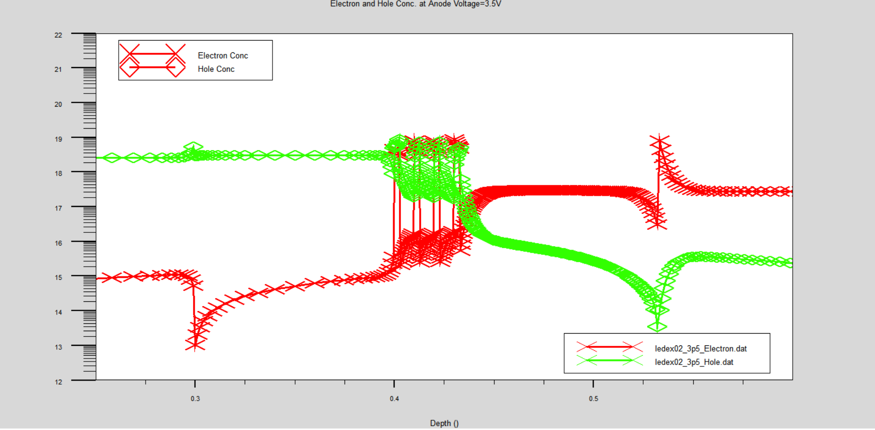
tonyplot -overlay ledex02_3p5_Electron.dat ledex02_3p5_Hole.dat -set ledex02_3.set
tonyplot -overlay ledex02_4p0_Electron.dat ledex02_4p0_Hole.dat -set ledex02_4.set
tonyplot -overlay ledex02_5p0_Electron.dat ledex02_5p0_Hole.dat -set ledex02_5.set2.2逐句解释
0.说明
# (c) Silvaco Inc., 2013
go atlas

# GaN LED Opto Device Simulation
#氮化镓LED光学设备仿真
# UltraViolet Multi-quantum well LED   紫外线多量子阱LED
# APL Vol.73 No.12. 21 Sep.(1998) pp.1688-1690
#来源?
# Parameter used for this UV MQW LED此UV MQW LED用到的参数
#############################################################################
#  Epilayer #  Material  #  Type  # Thickness #  Doping    #    Mobility    #
#           #            # p or n #     [nm]  #   [cm-3]   #    [cm2/V-s]   #
#############################################################################
# p-Contact #    GaN     #    p   #    100    #     1e20   #        10      #
# p-Emitter #  Al0.10GaN #    p   #    200    #     1e20   #        10      #
# p-Emitter #  Al0.20GaN #    p   #    100    #     1e20   #        10      #
#  4MQW     #    GaN     #    -   #      3    #       -    #       200      #
#  3Barrier #  Al0.2GaN  #    -   #      7    #       -    #       100      #
# n-Emitter #  Al0.2GaN  #    n   #    100    #     2e18   #       100      #
# n-Contact #    GaN     #    n   #    300    #     2e18   #       100      #
#############################################################################
网格
# 1 Dimensional Structure
# for A Cylindrical 120 diameter(3.14*60*60=1.13e4)
#对于直径为120的圆柱形(3.14*60*60=1.13e4)
mesh width=1.13e4
#
x.mesh loc=0.0   spac=0.5
x.mesh loc=1.0   spac=0.5
#
y.mesh loc=0.0   spac=0.05
y.mesh loc=0.1   spac=0.001
y.mesh loc=0.2 spac=0.025
y.mesh loc=0.3   spac=0.001
y.mesh loc=0.35 spac=0.01
y.mesh loc=0.4   spac=0.0005
y.mesh loc=0.433 spac=0.0005
y.mesh loc=0.483 spac=0.001
y.mesh loc=0.533 spac=0.001
y.mesh loc=2.033 spac=0.10
y.mesh loc=3.533 spac=0.01
#
mesh width有什么意义?之前没怎么注意过?
这网格整体形状还挺好看
2.区域定义
#
region number=1 y.max=0.1 material=GaN
region number=2 y.min=0.1 y.max=0.3 material=AlGaN x.comp=0.1
region number=3 y.min=0.3 y.max=0.4 material=AlGaN x.comp=0.2
#
# 4 MQW
#
region number=4 y.min=0.4 y.max=0.403 material=GaN name=well led qwell
region number=5 y.min=0.403 y.max=0.410 material=AlGaN x.comp=0.2
region number=6 y.min=0.410 y.max=0.413 material=GaN name=well led qwell
region number=7 y.min=0.413 y.max=0.420 material=AlGaN x.comp=0.2
region number=8 y.min=0.420 y.max=0.423 material=GaN name=well led qwell
region number=9 y.min=0.423 y.max=0.430 material=AlGaN x.comp=0.2
region number=10 y.min=0.430 y.max=0.433 material=GaN name=well led qwell
region number=11 y.min=0.433 y.max=0.533 material=AlGaN x.comp=0.2
region number=12 y.min=0.533 y.max=3.533 material=GaN substrate
#
3.电极和掺杂
#
electrode name=anode   top
electrode name=cathode bottom
#
doping region=1 uniform p.type conc=1e20
doping region=2 uniform p.type conc=1e20
doping region=3 uniform p.type conc=1e20
# doping 4~10 intrinsic#固有不变,看一下组分
doping region=11 uniform n.type conc=2e18
doping region=12 uniform n.type conc=2e18
#
电极:
掺杂:
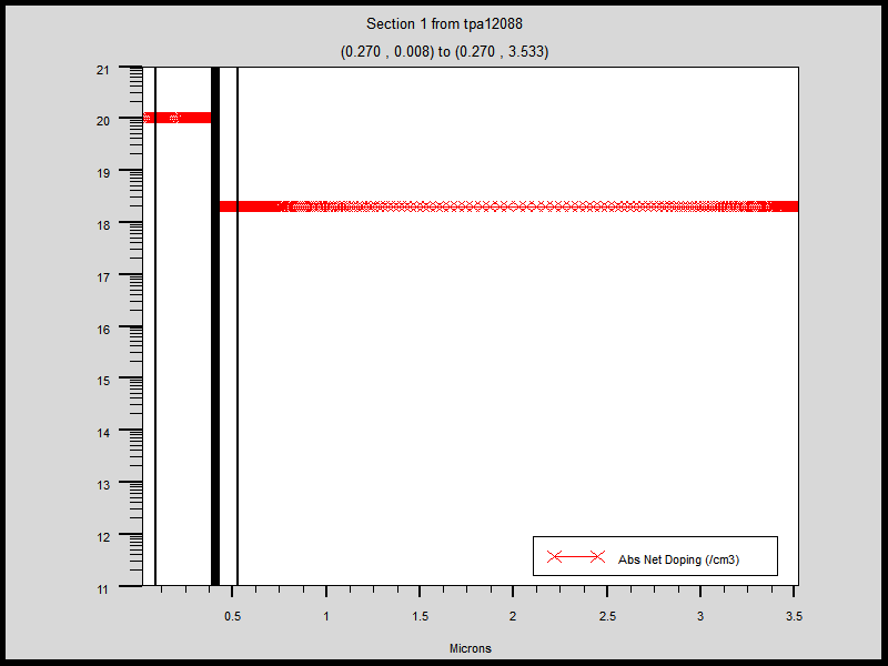
4-10组分
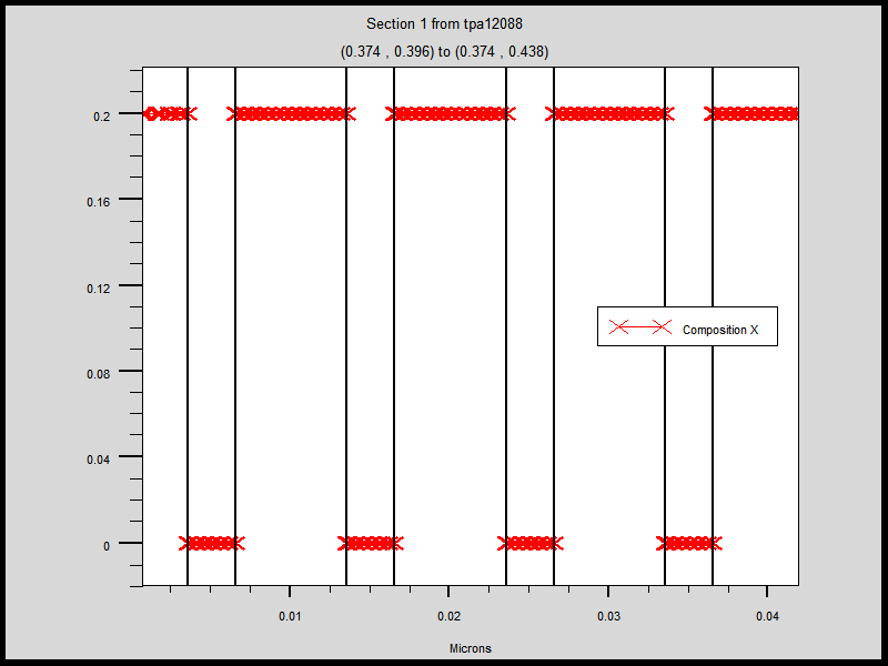
从上图可看出,绘制过后纵坐标都变了,得看cutline的原图。
4.模型和材料
#模型定义
models polarization calc.strain polar.scale=0.15
#应变和极化
material material=GaN taun0=1e-9 taup0=1e-9 copt=1.1e-8 \
         augn=1.0e-34 augp=1.0e-34
material material=AlGaN taun0=1e-9 taup0=1e-9 copt=1.1e-8 \
         augn=1.0e-34 augp=1.0e-34
material material=InGaN taun0=1e-9 taup0=1e-9 copt=1.1e-8 \
         augn=1.0e-34 augp=1.0e-34
# 1
material well.gamma0=10e-3
#1
material edb=0.080 eab=0.101
#1
models k.p fermi incomplete consrh auger optr print
models name=well k.p chuang spontaneous lorentz
#1
mobility material=GaN mun0=300 mup0=10
mobility material=AlGaN mun0=250 mup0=5
同例子一,应变和极化模型,参数略有不同
GaN:taun0(SRH 复合的电子寿命s)=1e-9
taup0(SRH 复合的空穴寿命s)=1e-9
copt=1.1e-8 材料的光学复合速率(cm3/s),设定模型时需使用 model optr
augn=1.0e-34 电子俄歇系数(cm6/s);
augp=1.0e-34 空穴俄歇系数(cm6/s)
AlGaN:略
InGaN:略
material well.gamma0=10e-3
well.gamma0还是洛伦兹增益扩大模型的参数,GAMMA0在材料语句中可由用户指定。

指定了“洛伦兹增益增宽”中的洛伦兹增益增宽因子。
material edb=0.080 eab=0.101
edb指定施主(donor)能级 eab :指定受主(acceptor)能级
models k.p fermi incomplete consrh auger optr print
models name=well k.p chuang spontaneous lorentz
同led1
mobility material=GaN mun0=300 mup0=10
mobility material=AlGaN mun0=250 mup0=5
设定GaN AlGaN电子和空穴迁移率
5.输出、初值和探针设置
#1
output con.band val.band band.param charge polar.charge e.mobility h.mobility \
       u.srh u.radiative u.auger permi
#1
solve init
#1
method climit=1e-4 maxtrap=10
#block nblockit=50
#1
solve prev
#1
save outf=ledex02_1.str
#1
probe name="Radiative"     integrate radiative rname=well
probe name="Recombination" integrate recombination
#
output con.band val.band band.param charge polar.charge e.mobility h.mobility \
u.srh u.radiative u.auger permi
设定输出:导带、价带、……其他的具体还不太清楚
solve prev/init有什么区别呀
solve previous :将之前计算得到的结果作为计算的初始近似
probe name="Radiative" integrate radiative rname=well
probe name="Recombination" integrate recombination
Probe—点 Probe 菜单,然后用左键在 Tonyplot 显示区域点击某一“点”就可获得该点
的信息。如果点在网格的同一个三角形内,那么显示的结果会是相同的,而不是所认为的点
的坐标不同结果就不同。这就是网格离散化带来的必然结果,意识到这一点将帮助你更深入
地理解 TCAD 的精髓。
probe 状态允许输出日志文件中保存特定位置的分立的值,例输出 potential。
log outf=ledex02.log
solve vstep=0.1 vfinal=2.5 name=anode
save outf=ledex02_2p5.str
save spectrum=ledex02_2p5.spc lmin=0.33 lmax=0.38 nsamp=100

solve vstep=0.1 vfinal=3.0 name=anode
save outf=ledex02_3p0.str
save spectrum=ledex02_3p0.spc lmin=0.33 lmax=0.38 nsamp=100

solve vstep=0.1 vfinal=3.5 name=anode
save outf=ledex02_3p5.str
save spectrum=ledex02_3p5.spc lmin=0.33 lmax=0.38 nsamp=100

solve vstep=0.1 vfinal=4.0 name=anode
save outf=ledex02_4p0.str
save spectrum=ledex02_4p0.spc lmin=0.33 lmax=0.38 nsamp=100

solve vstep=0.1 vfinal=5.0 name=anode
save outf=ledex02_5p0.str

solve vstep=0.1 vfinal=6.0 name=anode
save outf=ledex02_6p0.str
#
# V-I Curve
tonyplot ledex02.log -set ledex02_0.set
# I-L Curve
tonyplot ledex02.log -set ledex02_1.set
# EL Spectrum
tonyplot ledex02_3p5.spc -set ledex02_2.set
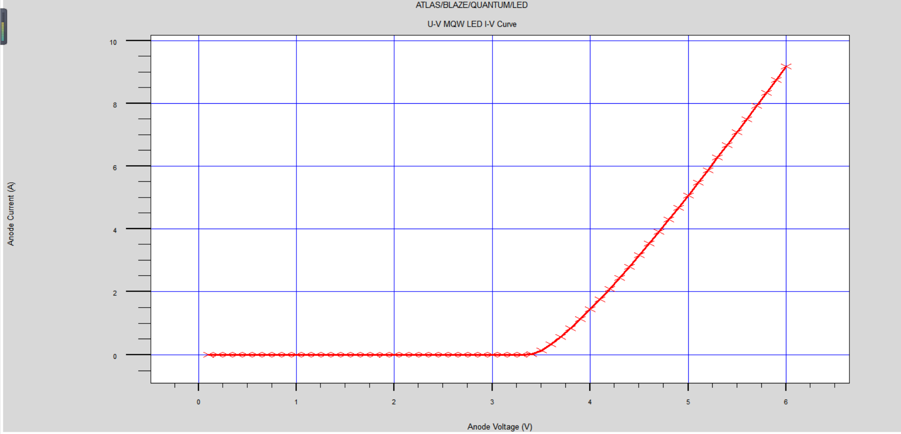

# V-I Curve
tonyplot ledex02.log -set ledex02_0.set
# I-L Curve
tonyplot ledex02.log -set ledex02_1.set
# EL Spectrum
tonyplot ledex02_3p5.spc -set ledex02_2.set

# Extract the Electron And hole Conc.
extract init infile="ledex02_3p5.str"
extract name="Electron" curve(depth,impurity="Electron Conc" material="All" \
        x.val=0.5) outfile="ledex02_3p5_Electron.dat"
extract name="Electron" curve(depth,impurity="Hole Conc" material="All" \
        x.val=0.5) outfile="ledex02_3p5_Hole.dat"

extract init infile="ledex02_4p0.str"
extract name="Electron" curve(depth,impurity="Electron Conc" material="All" \
        x.val=0.5) outfile="ledex02_4p0_Electron.dat"
extract name="Electron" curve(depth,impurity="Hole Conc" material="All" \
        x.val=0.5) outfile="ledex02_4p0_Hole.dat"

extract init infile="ledex02_5p0.str"
extract name="Electron" curve(depth,impurity="Electron Conc" material="All" \
        x.val=0.5) outfile="ledex02_5p0_Electron.dat"
extract name="Electron" curve(depth,impurity="Hole Conc" material="All" \
        x.val=0.5) outfile="ledex02_5p0_Hole.dat"

tonyplot -overlay ledex02_3p5_Electron.dat ledex02_3p5_Hole.dat  -set ledex02_3.set

tonyplot -overlay  ledex02_4p0_Electron.dat ledex02_4p0_Hole.dat -set ledex02_4.set

tonyplot -overlay  ledex02_5p0_Electron.dat ledex02_5p0_Hole.dat -set ledex02_5.set


 7589
7589


 被折叠的 条评论
为什么被折叠?
被折叠的 条评论
为什么被折叠?
 到【灌水乐园】发言


