


对于XILINX,7系列FPGA,关于GTX核对配置见PG168,了解GTX内部结构及更多的知识见ug476。
以7系列XC7k325t-ffg900为例,见各ug476,351页。可看到该芯片共有4个高速bank,分别为115 116 117 118;每个bank又有4组收发模块和两组时钟模块。
1,GTX时钟和复位
(1)时钟源:
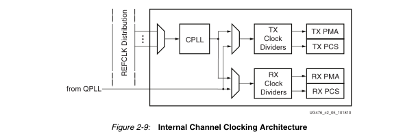
GTX输入参考时钟通过2组时钟模块的任意一组输入.后通过 IBUFDS_GTE2源于得到参考时钟输入给GT模块.。此处有两种PLL由Xilinx提供给用户使用。一种为CPLL,一种为QPLL,其中主要区别为CPLL一个bank中共有4个,一个收发模块一个;而QPLL只有两个,一个时钟模块对应一个。从GTX速率而言,CPLL主要用低于6.25G速率的收发设计;而QPLL主要支持高于6.25G低于10.3025G速率的收发器设计。
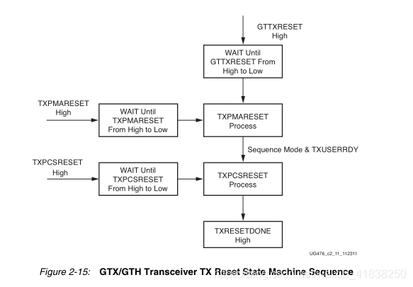
(2)发送端初始化复位:
在时钟CPLL或QPLL时钟locked拉高(表示时钟稳定,可以正常工作)。通过GTTXRESET复位GT发送器,发送器收到复位信号从底层PMA到PCS依次复位。在PMA层,待TXPMAREAET从高变成低通过PMA层,待TXUSERRDY为高,到达PCS层;在PCS层,待TXPCSREAET从高变成低通过PCS层,则TXREAETDONE拉高,发送器复位完成。之后发送复位状态机完成复位,输出发送状态机复位完成信号。复位关系和时序如图所示:

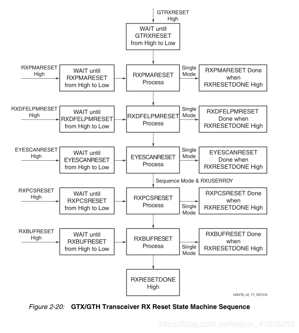
(3)接收端初始化复位:
在时钟CPLL或QPLL时钟locked拉高(表示时钟稳定,可以正常工作)。通过GTRXRESET复位GT接收器,接收器收到复位信号从底层PMA到到DFE,LPM到EYESCAN到PCS到BUF依次复位。在PMA层,待RXPMAREAET从高变成低通过PMA层,RXPMARESETDONE拉高;到达DFELPM层,待RXDFELPMRESET从高变成低通过DFE LPM层,RXDFE LPMRESETDONE拉高;到达EYECAN层,待RXEYECANRESET从高变成低通过EYECAN层,RXEYECANRESETDONE拉高;待RXUSERRDY为高;到达PCS层;在PCS层,待RXPCSREAET从高变成低通过PCS层,则RXPCSREAETDONE拉高;到达BUF层,待RXBUFRESET从高变成低通过BUF层,RXBUFRESETDONE拉高;最后RXRESETDONE拉高;接收器复位完成。之后接收复位状态机完成复位,输出接收状态机复位完成信号。复位关系和时序如图所示:

2,GTX发送器
FPGA内部每一个收发器都有一个独立的发送端,发送端由PMA,PCS组成;由图可以看出PMA层包括并串转换,预加重,均衡,时钟发生器等;PCS层包括 8B/10B编码,数据缓冲区等。具体如图所示:
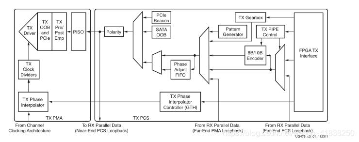
interface用户接口:使能8B/10B,数据位宽可以为:16,32,64;不使能8B/10B,数据位宽可以为:16,20,32,40,64,80;时钟=线速率/(8B/10B编码后的数据位宽);
8B/10B编码:保证时钟恢复,提供数据对齐,保持良好的直流平衡;
tx buffer :主要用户消除两个时钟直接的相位差;也可以不用;
tx pattern generator : 通过伪随机数来扩频;
tx polarity control : 如果P N接反,则通过配置该为矫正;
3,GTX接收器
接收器和发送器的数据流相反,接收器需要恢复时钟,补偿数据,恢复数据,串并转换,再8B/10B解码;最后输出数据给用户接口;如图:
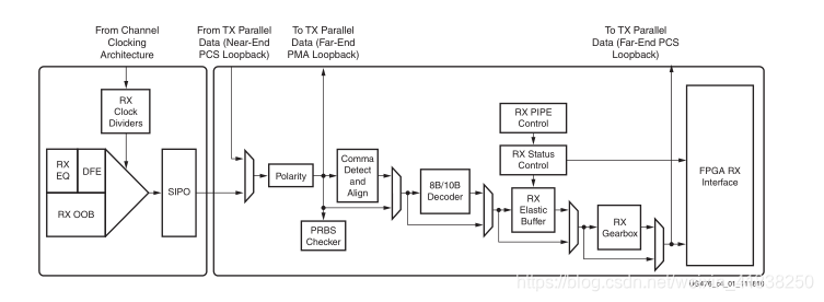
DFE和LPM : 数据到达接收器后,先经过RX均衡器,均衡器主要用于补偿信号在信道传输过程中的高频损失;DFE和LPM是接收器中的两种均衡器,LPM功耗较低,DFE能提供更精准的滤波参数。
RX,CDR : 时钟恢复电路, 接收端需要恢复时钟和数据,主要通过这个模块实现时钟,数据恢复。
其余模块都与发送端类似。
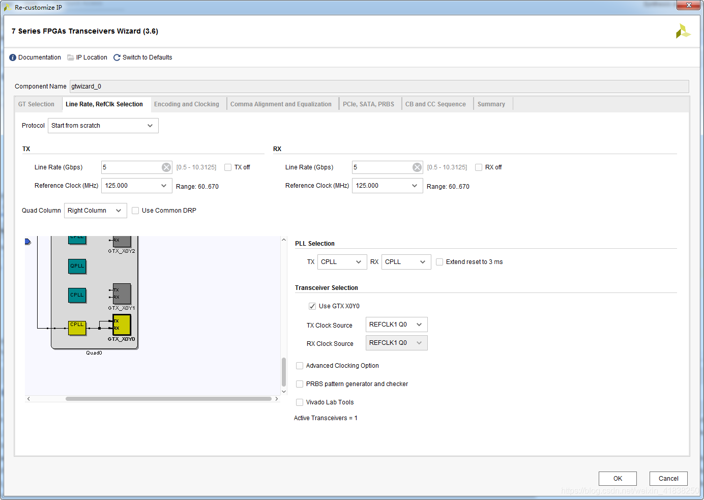
4,IP配置(以XC7K325T-FFG900为例)
(1) IP配置有两种方式选择。 有两种方式: 一种完成集成与IP核,只需要列化一个模块就能可以,但是这种种方式不太灵活,如果多通道并用,可能不好处理,还有一种核心模块为IP,其余使用例程,参考例程设计。具体选择可根据具体需求来实现:(我的设计中采用了只使用核心IP,其余参考例程设计)
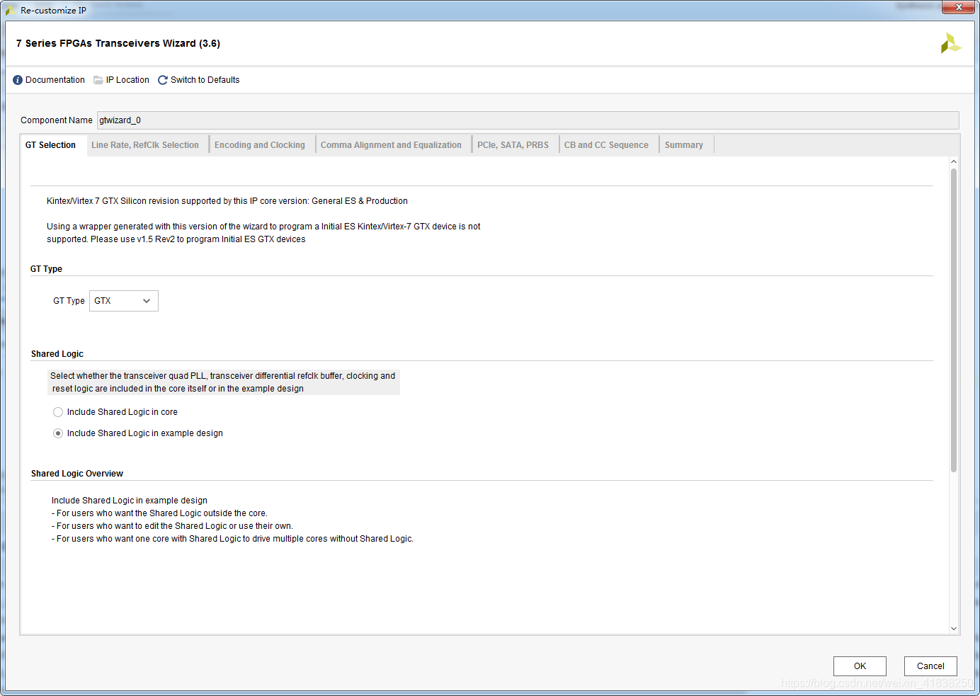
(2)主要配置页
protocol : 协议选择,GTX是高速串行收发器,在他的基础上可以很多的协议如SDI ,10Gbase,aurora,hdmi,sata等;
line rate :线速率配置,当前芯片最大支持10.3125G;
reference clock : 参考时钟,由外部输入,根据线速率选择合适的参考时钟输入;
pll selection :PLL选择;
transceiver selection:收发器选择,一个bank有4个收发器,根据项目需求,原理设计选择。
(3)8B/10B使能,BUF配置,por选择
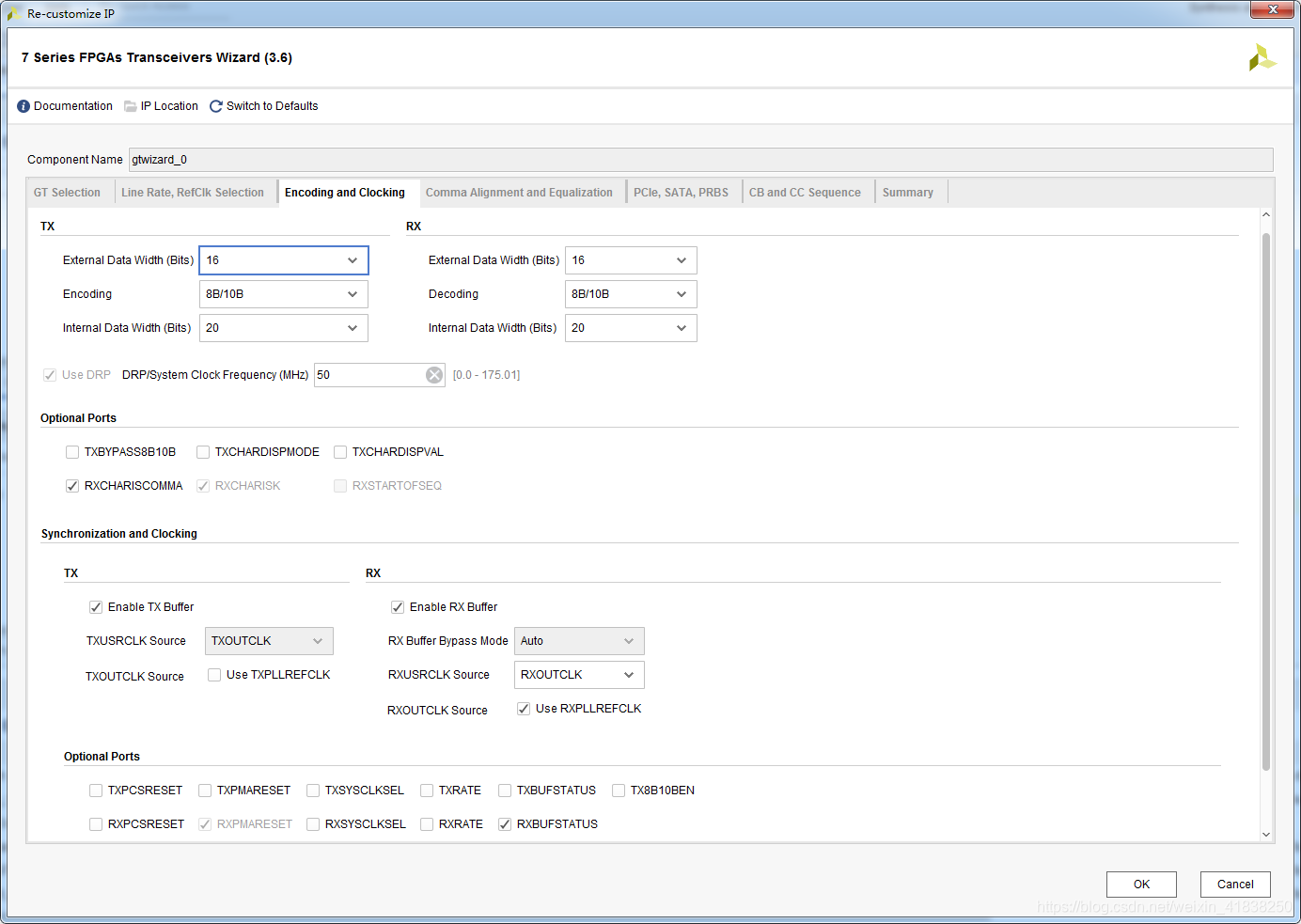
8B/10B : 根据设计选择8B/10B是否使能,配置数据位宽为16,32,64;
drpclk/sysclk : 系统时钟输入,复位信号等由该时钟产生;可输入0-175m时钟;
synchronization and clocking : 配置接收时钟,配置时钟源,是否使用buf;
optional port : 可以根据需求引出相关端口,以帮助IP核配置,控制使用。
(4)K码,均衡配置
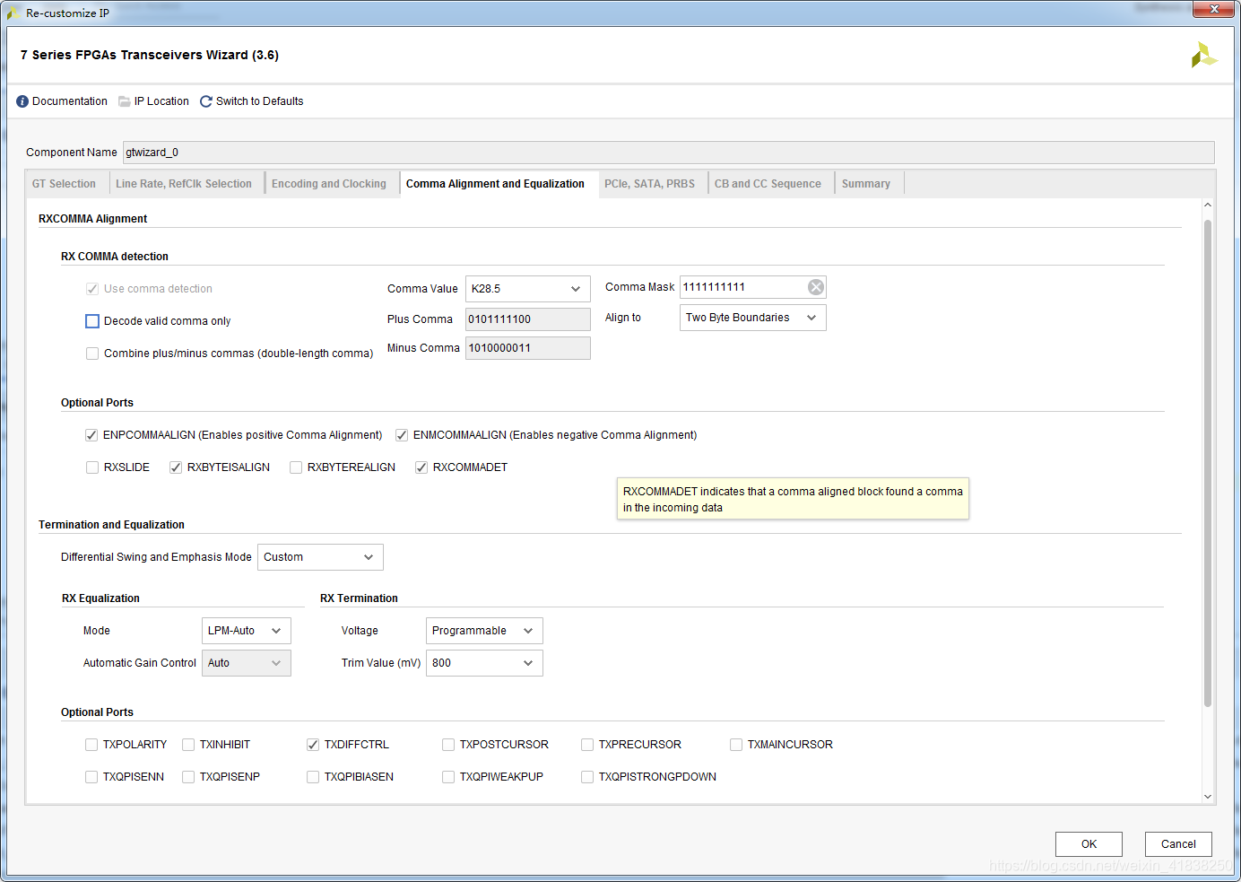
rx comma detection : 接收端对齐数据选择,可配置为2byte, 4byte 等。具体根据数据位宽决定;
termination and equalization : 均衡器配置,可配合ibert核使用,得到最合理的参数然后配置给IP核。
(5) 后面暂时不用管,直接下一步到最后完成配置。
5, 附上一个简单GT口配置逻辑,以便今后回顾。
// ____ ____
// / /\/ /
// /___/ \ / Vendor: Xilinx
// \ \ \/ Version : 3.6
// \ \ Application : 7 Series FPGAs Transceivers Wizard
// / / Filename : gtwizard_0_support.v
// /___/ /\
// \ \ / \
// \___\/\___\
//
//
// Module gtwizard_0_support
// Generated by Xilinx 7 Series FPGAs Transceivers Wizard
//
//
// (c) Copyright 2010-2012 Xilinx, Inc. All rights reserved.
//
// This file contains confidential and proprietary information
// of Xilinx, Inc. and is protected under U.S. and
// international copyright and other intellectual property
// laws.
//
// DISCLAIMER
// This disclaimer is not a license and does not grant any
// rights to the materials distributed herewith. Except as
// otherwise provided in a valid license issued to you by
// Xilinx, and to the maximum extent permitted by applicable
// law: (1) THESE MATERIALS ARE MADE AVAILABLE "AS IS" AND
// WITH ALL FAULTS, AND XILINX HEREBY DISCLAIMS ALL WARRANTIES
// AND CONDITIONS, EXPRESS, IMPLIED, OR STATUTORY, INCLUDING
// BUT NOT LIMITED TO WARRANTIES OF MERCHANTABILITY, NON-
// INFRINGEMENT, OR FITNESS FOR ANY PARTICULAR PURPOSE; and
// (2) Xilinx shall not be liable (whether in contract or tort,
// including negligence, or under any other theory of
// liability) for any loss or damage of any kind or nature
// related to, arising under or in connection with these
// materials, including for any direct, or any indirect,
// special, incidental, or consequential loss or damage
// (including loss of data, profits, goodwill, or any type of
// loss or damage suffered as a result of any action brought
// by a third party) even if such damage or loss was
// reasonably foreseeable or Xilinx had been advised of the
// possibility of the same.
//
// CRITICAL APPLICATIONS
// Xilinx products are not designed or intended to be fail-
// safe, or for use in any application requiring fail-safe
// performance, such as life-support or safety devices or
// systems, Class III medical devices, nuclear facilities,
// applications related to the deployment of airbags, or any
// other applications that could lead to death, personal
// injury, or severe property or environmental damage
// (individually and collectively, "Critical
// Applications"). Customer assumes the sole risk and
// liability of any use of Xilinx products in Critical
// Applications, subject only to applicable laws and
// regulations governing limitations on product liability.
//
// THIS COPYRIGHT NOTICE AND DISCLAIMER MUST BE RETAINED AS
// PART OF THIS FILE AT ALL TIMES.
`timescale 1ns / 1ps
module gt_wrap (
input sysclk_in,
input sysreset_in,
input clk1_gtrefclk_n,
input clk1_gtrefclk_p,
input [1:0] gtxrxp_in,
input [1:0] gtxrxn_in,
output [1:0] gtxtxn_out,
output [1:0] gtxtxp_out,
output qpll_locked,
output [1:0] rx_resetdone,
output [1:0] tx_resetdone,
output [1:0] tx_fsm_reset_done,
output [1:0] rx_fsm_reset_done,
output tx_clk,
output rx_clk,
output [7:0] rx_charisk,
output [63:0] rx_data,
input [7:0] tx_charisk,
input [63:0] tx_data,
input ctrl_loppback,
output [7:0] rx_disperr,
output [7:0] rx_notintable,
output [5:0] rx_bufstatus
);
genvar i ;
//qpll
wire commonreset_i;
wire gt0_qplllock_i;
wire gt0_qpllrefclklost_i ;
wire [1:0] gt0_qpllreset_i ;
wire gt0_qpllreset_t ;
wire gt0_qplloutclk_i ;
wire gt0_qplloutrefclk_i ;
//Reference Clocks
wire q0_clk1_refclk_i;
//User Clocks
wire [1:0] gt0_rxoutclk_i;
wire [1:0] gt0_txoutclk_i;
wire gt0_txusrclk_i;
wire gt0_rxusrclk_i;
wire gt0_txusrclk2_i;
wire gt0_rxusrclk2_i;
//**************************** Main Body of Code *******************************
assign qpll_locked = gt0_qplllock_i;
assign tx_clk = gt0_txusrclk2_i;
assign rx_clk = gt0_rxusrclk2_i;
gtwizard_0_GT_USRCLK_SOURCE gtwizard_0_GT_USRCLK_SOURCE (
.GT0_TXUSRCLK_OUT (gt0_txusrclk_i),
.GT0_TXUSRCLK2_OUT (gt0_txusrclk2_i ),
.GT0_TXOUTCLK_IN (gt0_txoutclk_i[0]),
.GT0_RXUSRCLK_OUT (gt0_rxusrclk_i),
.GT0_RXUSRCLK2_OUT (gt0_rxusrclk2_i ),
.GT0_RXOUTCLK_IN (gt0_rxoutclk_i[0]),
.Q0_CLK1_GTREFCLK_PAD_N_IN (clk1_gtrefclk_n),
.Q0_CLK1_GTREFCLK_PAD_P_IN (clk1_gtrefclk_p),
.Q0_CLK1_GTREFCLK_OUT (q0_clk1_refclk_i)
);
gtwizard_0_common #(
.WRAPPER_SIM_GTRESET_SPEEDUP("TRUE"),
.SIM_QPLLREFCLK_SEL(3'b010)
)
gtwizard_0_common (
.QPLLREFCLKSEL_IN(3'b010),
.GTREFCLK0_IN(1'b0),
.GTREFCLK1_IN(q0_clk1_refclk_i),
.QPLLLOCK_OUT(gt0_qplllock_i),
.QPLLLOCKDETCLK_IN(sysclk_in),
.QPLLOUTCLK_OUT(gt0_qplloutclk_i),
.QPLLOUTREFCLK_OUT(gt0_qplloutrefclk_i),
.QPLLREFCLKLOST_OUT(gt0_qpllrefclklost_i),
.QPLLRESET_IN(gt0_qpllreset_t)
);
assign gt0_qpllreset_t = commonreset_i | >0_qpllreset_i;
gtwizard_0_common_reset #(
.STABLE_CLOCK_PERIOD (8) // Period of the stable clock driving this state-machine, unit is [ns]
)
gtwizard_0_common_reset (
.STABLE_CLOCK(sysclk_in), //Stable Clock, either a stable clock from the PCB
.SOFT_RESET(sysreset_in), //User Reset, can be pulled any time
.COMMON_RESET(commonreset_i) //Reset QPLL
);
generate
for (i=0;i<2;i=i+1)
begin : gt_gen
gtwizard_0 gtwizard_0_init_i (
.sysclk_in (sysclk_in),
.soft_reset_tx_in (sysreset_in),
.soft_reset_rx_in (sysreset_in),
.dont_reset_on_data_error_in (1'b0),
.gt0_tx_fsm_reset_done_out (tx_fsm_reset_done[i]),
.gt0_rx_fsm_reset_done_out (rx_fsm_reset_done[i]),
.gt0_data_valid_in (1'b1),
//_____________________________________________________________________
//_____________________________________________________________________
//GT0 (X1Y0)
//-------------------------- Channel - DRP Ports --------------------------
.gt0_drpaddr_in (9'd0), // input wire [8:0] gt0_drpaddr_in
.gt0_drpclk_in (sysclk_in), // input wire sysclk_in_i
.gt0_drpdi_in (16'd0), // input wire [15:0] gt0_drpdi_in
.gt0_drpdo_out ( ), // output wire [15:0] gt0_drpdo_out
.gt0_drpen_in (1'b0), // input wire gt0_drpen_in
.gt0_drprdy_out ( ), // output wire gt0_drprdy_out
.gt0_drpwe_in (1'b0), // input wire gt0_drpwe_in
//------------------------- Digital Monitor Ports --------------------------
.gt0_dmonitorout_out ( ), // output wire [7:0] gt0_dmonitorout_out
//----------------------------- Loopback Ports -----------------------------
.gt0_loopback_in ({2'd0,ctrl_loppback }), // input wire [2:0] gt0_loopback_in
//------------------- RX Initialization and Reset Ports --------------------
.gt0_eyescanreset_in (1'b0), // input wire gt0_eyescanreset_in
.gt0_rxuserrdy_in (1'b0), // input wire gt0_rxuserrdy_in
//------------------------ RX Margin Analysis Ports ------------------------
.gt0_eyescandataerror_out ( ), // output wire gt0_eyescandataerror_out
.gt0_eyescantrigger_in (1'b0), // input wire gt0_eyescantrigger_in
//---------------- Receive Ports - FPGA RX Interface Ports -----------------
.gt0_rxusrclk_in (gt0_rxusrclk_i), // input wire gt0_rxusrclk_i
.gt0_rxusrclk2_in (gt0_rxusrclk_i), // input wire gt0_rxusrclk2_i
//---------------- Receive Ports - FPGA RX interface Ports -----------------
.gt0_rxdata_out (rx_data[32*i+:32]), // output wire [31:0] gt0_rxdata_out
//---------------- Receive Ports - RX 8B/10B Decoder Ports -----------------
.gt0_rxdisperr_out (rx_disperr[4*i+:4]), // output wire [3:0] gt0_rxdisperr_out
.gt0_rxnotintable_out (rx_notintable[4*i+:4]), // output wire [3:0] gt0_rxnotintable_out
//------------------------- Receive Ports - RX AFE -------------------------
.gt0_gtxrxp_in (gtxrxp_in[i]), // input wire gt0_gtxrxp_in
//---------------------- Receive Ports - RX AFE Ports ----------------------
.gt0_gtxrxn_in (gtxrxn_in[i]), // input wire gt0_gtxrxn_in
//----------------- Receive Ports - RX Buffer Bypass Ports -----------------
.gt0_rxbufstatus_out (rx_bufstatus[3*i+:3]), // output wire [2:0] gt0_rxbufstatus_out
//------------------- Receive Ports - RX Equalizer Ports -------------------
.gt0_rxdfelpmreset_in (1'b0), // input wire gt0_rxdfelpmreset_in
.gt0_rxmonitorout_out ( ), // output wire [6:0] gt0_rxmonitorout_out
.gt0_rxmonitorsel_in (1'b0), // input wire [1:0] gt0_rxmonitorsel_in
//------------- Receive Ports - RX Fabric Output Control Ports -------------
.gt0_rxoutclk_out (gt0_rxoutclk_i[i]), // output wire gt0_rxoutclk_i
.gt0_rxoutclkfabric_out ( ), // output wire gt0_rxoutclkfabric_out
//----------- Receive Ports - RX Initialization and Reset Ports ------------
.gt0_gtrxreset_in (1'b0), // input wire gt0_gtrxreset_in
.gt0_rxpmareset_in (1'b0), // input wire gt0_rxpmareset_in
//----------------- Receive Ports - RX8B/10B Decoder Ports -----------------
.gt0_rxcharisk_out (rx_charisk[4*i+:4]), // output wire [3:0] gt0_rxcharisk_out
//------------ Receive Ports -RX Initialization and Reset Ports ------------
.gt0_rxresetdone_out (rx_resetdone[i]), // output wire gt0_rxresetdone_out
//------------------- TX Initialization and Reset Ports --------------------
.gt0_gttxreset_in (1'b0), // input wire gt0_gttxreset_in
.gt0_txuserrdy_in (1'b0), // input wire gt0_txuserrdy_in
//---------------- Transmit Ports - FPGA TX Interface Ports ----------------
.gt0_txusrclk_in (gt0_txusrclk_i), // input wire gt0_txusrclk_i
.gt0_txusrclk2_in (gt0_txusrclk_i), // input wire gt0_txusrclk2_i
//---------------- Transmit Ports - TX Data Path interface -----------------
.gt0_txdata_in (tx_data[32*i+:32]), // input wire [31:0] gt0_txdata_in
//-------------- Transmit Ports - TX Driver and OOB signaling --------------
.gt0_gtxtxn_out (gtxtxn_out[i]), // output wire gt0_gtxtxn_out
.gt0_gtxtxp_out (gtxtxp_out[i]), // output wire gt0_gtxtxp_out
//--------- Transmit Ports - TX Fabric Clock Output Control Ports ----------
.gt0_txoutclk_out (gt0_txoutclk_i[i]), // output wire gt0_txoutclk_i
.gt0_txoutclkfabric_out ( ), // output wire gt0_txoutclkfabric_out
.gt0_txoutclkpcs_out ( ), // output wire gt0_txoutclkpcs_out
//------------------- Transmit Ports - TX Gearbox Ports --------------------
.gt0_txcharisk_in (tx_charisk[4*i+:4]), // input wire [3:0] gt0_txcharisk_in
//----------- Transmit Ports - TX Initialization and Reset Ports -----------
.gt0_txresetdone_out (tx_resetdone[i]), // output wire gt0_txresetdone_out
.gt0_qplllock_in(gt0_qplllock_i),
.gt0_qpllrefclklost_in(gt0_qpllrefclklost_i),
.gt0_qpllreset_out(gt0_qpllreset_i[i]),
.gt0_qplloutclk_in(gt0_qplloutclk_i),
.gt0_qplloutrefclk_in(gt0_qplloutrefclk_i)
);
end
endgenerate
endmodule
相关问题记录:
1,GTX时钟专用buf原语 :
IBUFDS_GTE2 IBUFDS_GTE2_inst (
.O(gtx_clk_out),
.ODIV2(),
.I(gtx_clk_in_p),
.CEB(1'b0),
.IB(gtx_clk_in_n)
);
2 ,光口接收时钟源配置一般有两种,使用RXOUTCLK,也可用RXOUTCLK;如果速率较高建议选择RXOUTCLK,保证数据和时钟同步,能更有效的保证数据采集。
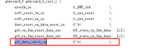
3,data_valid_in端口外部配置1,改信号主要影响接收复位状态机。
4, gtx数据接口为isk和dat;isk和dat按字节对应。


 2万+
2万+

 被折叠的 条评论
为什么被折叠?
被折叠的 条评论
为什么被折叠?
 到【灌水乐园】发言


