


1 FPGA启动流程
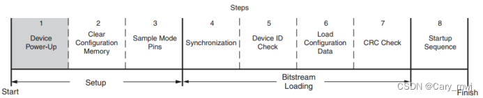
图 1 7 Serials FPGA配置流程
1.1 Device Power-Up
1.2 Clear Configuration Memory
在上电后的任何时间内,可以对Slave-FPGA配置存储器(Block RAM)进行复位处理。复位方式是将PROGRAM_B信号拉低(下降沿有效)。
1.3 Sample Mode Pins
当复位完成后,INIT_B恢复高电平,Slave-FPGA对M[2:0]模式引脚进行采样,然后开始在CCLK上升沿接收配置数据。
1.4 Synchronization
在接收配置数据前,Slave-FPGA首先进行总线位宽检测。主机发送的配置文件中,“Bus Width Auto Detection”序列最先发送。
表 1 Bus Width Detection Pattern
| D[24:31] | D[16:23] | D[8:15] | D[0:7] | Comments |
| 0xFF | 0xFF | 0xFF | 0xFF | |
| 0x00 | 0x00 | 0x00 | 0xBB | Bus Width Pattern |
| 0x11 | 0x22 | 0x00 | 0x44 | Bus Width Pattern |
| 0xFF | 0xFF | 0xFF | 0xFF | |
| 0xFF | 0xFF | 0xFF | 0xFF | |
| 0xAA | 0x99 | 0x55 | 0x66 | Sync word |
| 0xFF | 0xFF | 0xFF | 0xFF |
如上表,当位宽为8时,将在D[0:7]检测到0xBB、0x11;当位宽为16时,将在D[0:7]检测到0xBB、0x22;当位宽为32时,将在D[0:7]检测到0xBB、0x44。
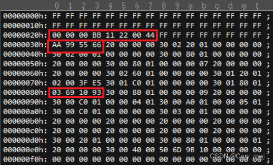
图 2 BIN文件内容
注意:表1中的数据为Bit-Swrap之后的数据(FPGA内部要求),而图2中的配置文件为非Bit-Swrap的数据,因此在实际的配置过程中,应将数据进行Bit-Swrap处理。
位宽检测完成后,需要进行同步检测。如表1与图2,同步序列为0xAA995566,经过Bit-Swrap处理后为0x5599AA66。
1.5 Device ID Check
同步之后需要进行ID检查以防止错误型号FPGA的比特流数据写入。如图2,0x03691093为ID号。
1.6 Load Configuration Data
ID检查成功后,Slave-FPGA开始接收配置数据。
1.7 CRC Check
当接收配置数据,Slave-FPGA进行CRC校验计算,当检验失败时将INT_B拉低。
1.8 Startup Sequence
当配置数据接收完毕后,比特流指示Slave-FPGA进入启动流程,并在启动完成后拉高DONE信号。
2 配置文件选择
表 2 Xilinx Configuration File Formats
| File Extension | Bit Swapping | Xilinx Tool | Description |
| BIT | Not Bit Swapped | ISE BitGen or Vivado write_bitstream (generated by default) | Binary configuration data file containing header information that does not need to be downloaded to the FPGA. Used to program devices from the iMPACT tool or Vivado device programmer with a programming cable. |
| RBT | Not Bit Swapped | ISE BitGen generated if -b option is set) or Vivado write_bitstream (generated with -raw_bitfile argument) | ASCII equivalent of the BIT file containing a text header and ASCII 1s and 0s. (Eight bits per configuration bit.) |
| BIN | Not Bit Swapped | ISE BitGen (generated if -g binary:yes option is set) or PROMGen, or Vivado write_bitstream (generated with -bin_file argument) | Binary configuration data file with no header information. Can be used for custom configuration solutions (for example, microprocessors), or in some cases to program third-party PROMs. |
| MCS | Not Bit Swapped | ISE PROMGen or iMPACT, or Vivado write_cfgmem -format MCS | ASCII PROM file format containing address and checksum information in addition to configuration data. Used mainly for device programmers and the Impact tool. |
| HEX | Not Bit Swapped | ISE PROMGen or iMPACT, or Vivado write_cfgmem -format HEX | ASCII PROM file format containing only configuration data. Used mainly in custom configuration solutions. |
根据表2说明,选择BIN文件作为配置文件。
3 Master SelectMAP模块设计

图 3 SelectMAP时序
图 4 selectmap端口定义
| 端口 | 位宽 | 方向 | 说明 | |
| I_clk | 1 | Input | 系统时钟 | |
| I_rst | 1 | Input | 系统复位 | |
| I_init | 1 | Input | 开始配置触发信号 | |
| O_init_done | 1 | Output | Slave-FPGA复位完成信号 | |
| SelectMAP Bus | O_mode | 3 | Output | Slave-FPGA配置模式选择 3’b000:Master Serial 3’b001:Master SPI 3’b010:Master BPI 3’b100:Master SelectMAP 3’b101:JTAG 3’b110:Slave SelectMAP 3’b111:Slave Serial |
| O_fpga_program_b | 1 | Output | Slave-FPGA配置逻辑复位(下降沿有效) | |
| I_fpga_int_b | 1 | Input | 指示Slave-FPGA配置逻辑复位完成(低有效),拉高后mode设置生效 | |
| O_fpga_cs_b | 1 | Output | 片选 1’b1:Enable SelectMAP bus 1’b0:Disable SelectMAP bus | |
| O_fpga_cclk | 1 | Output | 配置时钟 | |
| O_fpga_rdwr_b | 1 | Output | 读写控制 1’b1:Reading from Slave-FPGA 1’b0:Writing to Slave-FPGA | |
| O_fpga_data | 16 | Output | 配置数据 | |
| I_fpga_done | 1 | Input | Slave-FPGA加载完成 | |
| I_fifo_empty | 1 | Input | fifo空信号 | |
| O_fifo_rd_en | 1 | Output | fifo读使能 | |
| I_fifo_rd_data | 16 | Input | fifo读数据 | |
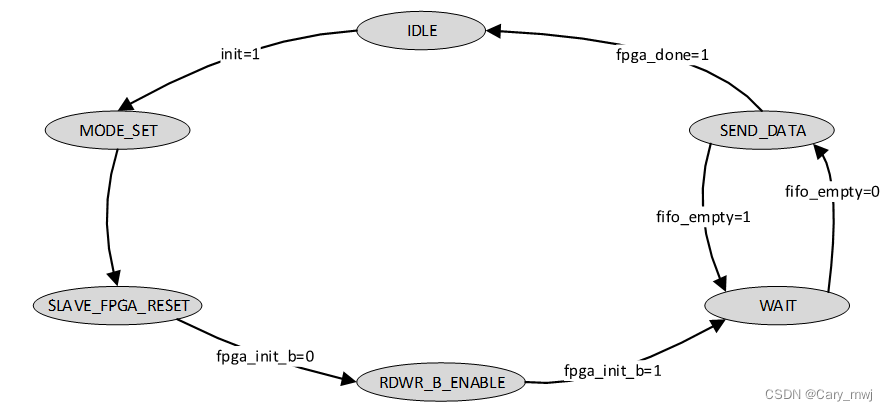
图 5 selectmap模块状态机
配置流程如下:
①在IDLE状态下,若检测到I_init为高,进入MODE_SET状态;
②在MODE_SET状态下,配置Slave-FPGA的模式为Slave SelectMAP模式(mode=3’b110),进入SLAVE_FPGA_RESET状态;
③在SLAVE_FPGA_RESET状态下,将fpga_program_b拉低以复位从设备配置逻辑;检测到fpga_int_b为低(复位完成)后,将fpga_program_b拉高,并拉低写使能fpga_rdwr_b,进入RDWR_B_ENABLE状态;
④在RDWR_B_ENABLE状态下,若检测到fpga_int_b由低变高(Slave-FPGA复位完成,等待数据写入),进入WAIT状态;
⑤在WAIT状态下,等待fifo加载数据;当fifo非空时,重新进入SEND_DATA状态发送数据;
⑥ 在SEND_DATA状态下,将来自fifo的配置数据加载到数据端口;
当检测到fpga_done为高时,配置完成,进入IDLE状态;
当检测到fpga_done为低且fifo为空时,进入WAIT状态。


 537
537


 被折叠的 条评论
为什么被折叠?
被折叠的 条评论
为什么被折叠?
 到【灌水乐园】发言


