


#学习记录#
1 DDS ip核介绍
打开IP catalog搜索DDS,选择DDS ip核打开如图1所示。
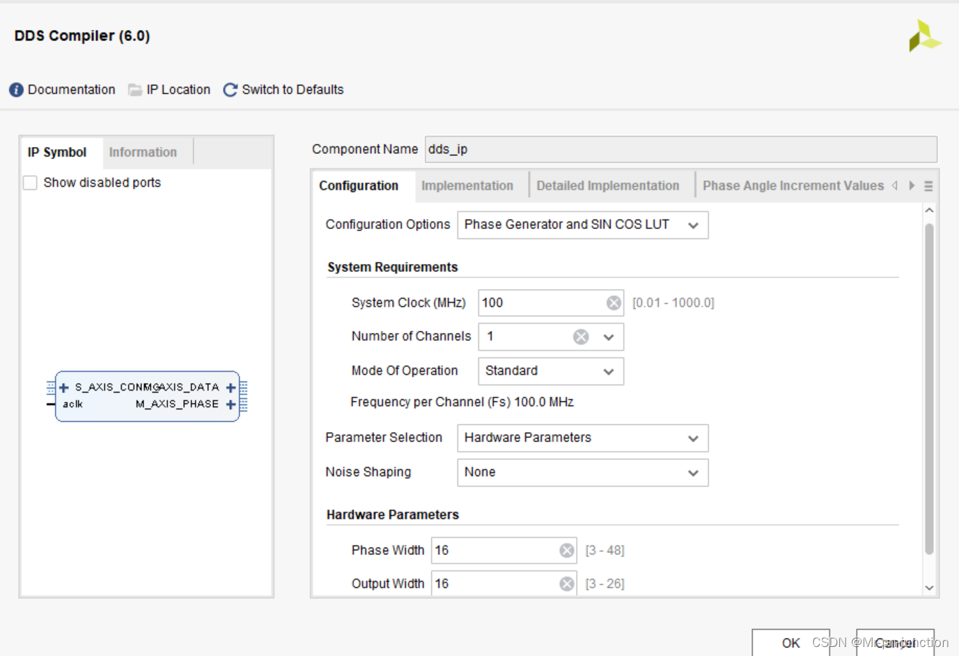
图1
configuration options有3种模式如下:
Phase Generator and SIN/COS LUT (DDS):相位和sin和cos的数据都是IP核自己产生
Phase Generator only:只要相位输出
SIN/COS LUT only模式:只需要sin/cos模块输出,但此模式需要外部不断的输入累加的相位
system clock:系统的时钟频率
number of channels:通道数
Mode of Operation: The DDS supports standard mode where the accumulated phase can be truncated before being used to access the SIN/COS LUT, or rasterized mode which can be used when the desired frequencies and system clock are related by a rational fraction.
Modulus (rasterized mode only): Describes the relationship between the system clock frequency and the desired frequencies. See Theory of Operation in Chapter 3 for more details.
Parameter Selection: DDS key parameters can be specified using System Parameters, which are aimed at system architects (frequency domain parameters) or Hardware Parameters, which are aimed at hardware engineers (time-domain parameters). The Phase Generator and SIN/COS LUT are only specified in terms of Hardware parameters.
输出频率计算:
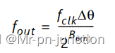
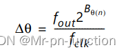
图2
Phase Increment Programmability:频率控制字。Fiexd(固定模式)需要在第四个配置页,配置输出的频率。
Programmable(可编程模式)
Phase Offset Programmability:相位控制字
Output: sin、cos、sin&cos这里选sin
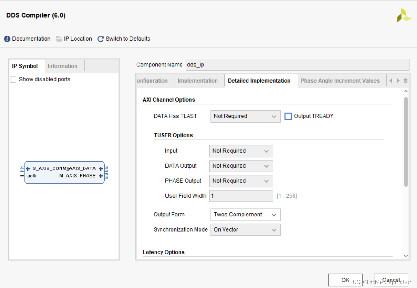
图3
Detailed Implementation:设置输入输出的一些格式,需不需要ready,last等,根据需要选择即可。
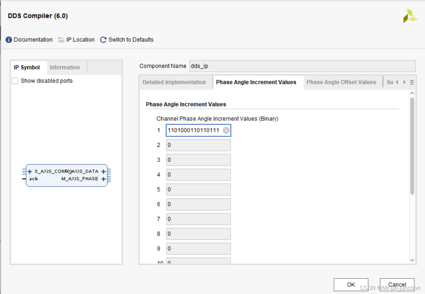
图4
Output Frequencies:输出频率,固定模式的时候设置这个,此处不需要。
2 DDS代码与仿真
2.1 代码
`timescale 1ns / 1ps
//
// Company:
// Engineer: mr-pn-junction
//
// Create Date: 2024/04/10 19:10:46
// Design Name:
// Module Name: DDS
// Project Name:
// Target Devices:
// Tool Versions:
// Description:
//
// Dependencies:
//
// Revision:
// Revision 0.01 - File Created
// Additional Comments:
//
//


module DDS(
    input sys_clk,
    input rst_n,
    input config_valid,
    input  [15:0]       config_data_pinc,
    output [15:0]       dds_data_sin

    );
    wire         m_axis_data_tvalid;
    wire         m_axis_phase_tvalid;
    wire [15:0]  m_axis_phase_tdata;

dds_ip dda_ip_0 (
      .aclk(sys_clk),                                  // input wire aclk
      .s_axis_config_tvalid(config_valid),            // input wire s_axis_config_tvalid
      .s_axis_config_tdata({16'b0,config_data_pinc}), // input wire [31 : 0] s_axis_config_tdata
      .m_axis_data_tvalid(m_axis_data_tvalid),      // output wire m_axis_data_tvalid
      .m_axis_data_tdata(dds_data_sin),  // output wire [15 : 0] m_axis_data_tdata
      .m_axis_phase_tvalid(m_axis_phase_tvalid),    // output wire m_axis_phase_tvalid
      .m_axis_phase_tdata(m_axis_phase_tdata)      // output wire [15 : 0] m_axis_phase_tdata
    );
endmodule
2.2 仿真文件
`timescale 1ns / 1ps
//
// Company:
// Engineer:mr-pn-junction
//
// Create Date: 2024/04/11 09:17:18
// Design Name:
// Module Name: dds_tb
// Project Name:
// Target Devices:
// Tool Versions:
// Description:
//
// Dependencies:
//
// Revision:
// Revision 0.01 - File Created
// Additional Comments:
//
//


module dds_tb();
    reg sys_clk;
    always #5 sys_clk = ~sys_clk;
    reg rst_n;
    wire [15:0]       dds_data_sin;
    reg  [15:0]       config_data_pinc;
    reg               config_valid;
DDS dds_u(
    .sys_clk(sys_clk),
    .rst_n(rst_n),
    .dds_data_sin(dds_data_sin),
    .config_data_pinc(config_data_pinc),
    .config_valid(config_valid)
);
initial begin
    sys_clk = 0;
    rst_n = 1;
    config_data_pinc = 16'd66;
    config_valid = 1'b1;
    #100000
    config_data_pinc = 16'd666;
    #100000
    $stop;
end
endmodule
3 仿真结果
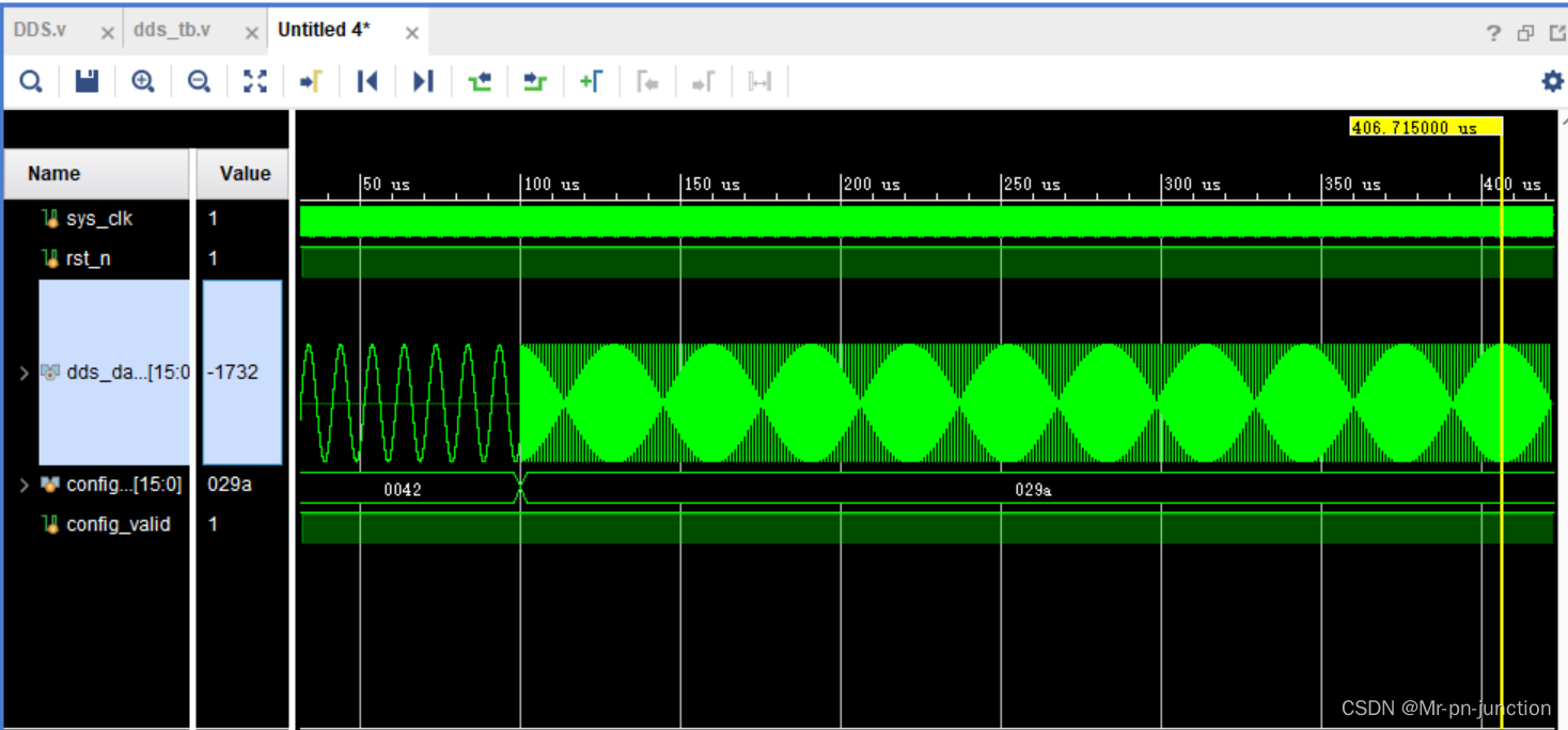
图5
在100us之后改变了正弦波的频率,如图5所示。
4 遇到的问题
Q:在进行behavioral simulation时候我们得到的正弦波可能如图6所示。
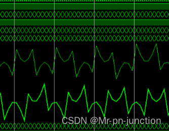
图6
解决办法:要想观察到正余弦信号,需要将Radix 修改为 signed Decimal即可。
参考文献:
[1] Vivado DDS IP使用的时候波形不是正弦波_为什么不能生成正弦波vivado-CSDN博客
[2] vivado DDS IP核的使用及仿真_vivoda仿真ip核-CSDN博客
[3] DDS ip手册DDS Compiler v6.0 Product Guide (PG141) • 查看器 • AMD 技术信息门户
[4] vivado2018.3调用DDS IP 讲解及仿真实例.BandpassFilter.vivado2018.3调用DDS IP 讲解及仿真实例_哔哩哔哩_bilibili


 2367
2367


 被折叠的 条评论
为什么被折叠?
被折叠的 条评论
为什么被折叠?
 到【灌水乐园】发言


