信号完整性的常见术语概念(面试常用)

目录

术语

概念一览

1.信号完整性(Signal Integrity)

2.传输线(Transmission Line)

3.特性阻抗(Characteristic Impedance)

4.反射(Reflection)

5.串扰(Crosstalk)

6.过冲(Overshoot)

7.下冲(Undershoot)

8.电路延迟

9.边沿时间

10.占空比偏斜

11.输出到输出偏斜

12.器件到器件偏斜

13.动态偏斜


术语

概念一览

1.信号完整性(Signal Integrity

        信号完整性是指信号在信号线上的质量。信号具有良好的信号完整性是指当在需要的时候具有所必需达到的电压电平数值。

2.传输线(Transmission Line

        传输线是一个网络(导线),并且它的电流返回到地或电源。

3.特性阻抗(Characteristic Impedance

        组成信号传输回路的两个导体之间存在分布电感和分布电容,当信号沿该导体传输时, 信号的跃变电压(V)和跃变电流( I )的比值称为特性阻抗( Z 0 ),即 Z 0 =V/I

4.反射Reflection

        反射就是在传输线上的回波。信号功率(电压和电流)的一部分传输到线上并达到负载处,但是有一部分被反射了。如果源端与负载端具有相同的阻抗,反射就不会发生。

5.串扰Crosstalk

        串扰是两条信号线之间的耦合。信号线之间的互感和互容引起线上的噪声。容性耦合引发耦合电流,而感性耦合引发耦合电压。
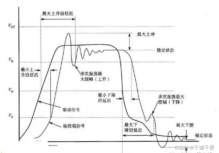
6.过冲Overshoot

        过冲就是第一个峰值或谷值超过设定电压。对于上升沿是指最高电压,而对于下降沿是指最低电压。过分的过冲能够引起保护二极管工作,导致过早地失效。

7.下冲Undershoot

        下冲是指下一个谷值或峰值。过分的下冲能够引起假的时钟或数据错误(误操作)。

8.电路延迟

指信号在器件内传输所需的时间( T pd ) 。例如, TTL 的电路延迟在 3 ~ 20nS 范围。

9边沿时间

        器件输出状态从逻辑低电平跃变到高电平所需要的时间(信号波形的 10~90% ),通常表示为上升沿(T r )。器件输出状态从逻辑高电平下降到低电平所需要的时间(信号波形的 90~10% ),通常表示为下降沿( T f )。

10.占空比偏斜

        信号传输过程中,从低电平到高电平的转换时间与从高电平到低电平的转换时间之间的差别,称为占空比偏斜。TTL和 CMOS 信号的占空比偏斜问题较为突出,主要是因为其输出的上升沿和下降沿延迟不同。

11.输出到输出偏斜

        同一器件不同输出引脚之间的信号延迟差别,称为输出到输出偏斜。

12.器件到器件偏斜

        由于制造工艺和使用环境的变化,造成的不同器件对应引脚之间的信号延迟差别,称为器件到器件偏斜。通常,器件之间的偏差远大于其他类型的偏斜。

13.动态偏斜

        主要是指由于温度变化、地或电源噪声造成阀值电平随时间漂移,从而产生信号延迟的变化。
Publisher: Prentice Hall PTR Pub Date: September 15, 2003 ISBN: 0-13-066946-6 Pages: 608 Section 2.7. The Spectrum of an Ideal Square Wave Section 2.8. From the Frequency Domain to the Time Domain Section 2.9. Effect of Bandwidth on Rise Time Section 2.10. Bandwidth and Rise Time Section 2.11. What Does "Significant" Mean? Section 2.12. Bandwidth of Real Signals Section 2.13. Bandwidth and Clock Frequency Section 2.14. Bandwidth of a Measurement Section 2.15. Bandwidth of a Model Section 2.16. Bandwidth of an Interconnect Section 2.17. Bottom Line Chapter 3. Impedance and Electrical Models Section 3.1. Describing Signal-Integrity Solutions in Terms of Impedance Section 3.2. What Is Impedance? Section 3.3. Real vs. Ideal Circuit Elements Section 3.4. Impedance of an Ideal Resistor in the Time Domain Section 3.5. Impedance of an Ideal Capacitor in the Time Domain Section 3.6. Impedance of an Ideal Inductor in the Time Domain Section 3.7. Impedance in the Frequency Domain Section 3.8. Equivalent Electrical Circuit Models Section 3.9. Circuit Theory and SPICE Section 3.10. Introduction to Modeling Section 3.11. The Bottom Line Chapter 4. The Physical Basis of Resistance Section 4.1. Translating Physical Design into Electrical Performance Section 4.2. The Only Good Approximation for the Resistance of Interconnects Section 4.3. Bulk Resistivity Section 4.4. Resistance per Length Section 4.5. Sheet Resistance Section 4.6. The Bottom Line Chapter 5. The Physical Basis of Capacitance Section 5.1. Current Flow in Capacitors Section 5.2. The Capacitance of a Sphere Section 5.3. Parallel Plate Approximation Section 5.4. Dielectric Constant Section 5.5. Power and Ground Planes and Decoupling Capacitance Section 5.6. Capacitance per Length Section 5.7. 2D Field Solvers Section 5.8. Effective Dielectric Constant Section 5.9. The Bottom Line Chapter 6. The Physical Basis of Inductance Section 6.1. What Is Inductance? Section 6.2. Inductance Principle #1: There Are Circular Magnetic-Field Line Loops Around All Currents Section 6.3. Inductance Principle #2: Inductance Is the Number of Webers of Field Line Loops Around a Conductor per Amp of Current Through It Section 6.4. Self-Inductance and Mutual Inductance Section 6.5. Inductance Principle #3: When the Number of Field Line Loops Around a Conductor Changes, There Will Be a Voltage Induced Across the Ends of the Conductor Section 6.6. Partial Inductance Section 6.7. Effective, Total, or Net Inductance and Ground Bounce Section 6.8. Loop Self- and Mutual Inductance Section 6.9. The Power-Distribution System (PDS) and Loop Inductance Section 6.10. Loop Inductance per Square of Planes Section 6.11. Loop Inductance of Planes and Via Contacts Section 6.12. Loop Inductance of Planes with a Field of Clearance Holes Section 6.13. Loop Mutual Inductance Section 6.14. Equivalent Inductance Section 6.15. Summary of Inductance Section 6.16. Current Distributions and Skin Depth Section 6.17. High-Permeability Materials Section 6.18. Eddy Currents Section 6.19. The Bottom Line Chapter 7. The Physical Basis of Transmission Lines Section 7.1. Forget the Word Ground Section 7.2. The Signal Section 7.3. Uniform Transmission Lines Section 7.4. The Speed of Electrons in Copper Section 7.5. The Speed of a Signal in a Transmission Line Section 7.6. Spatial Extent of the Leading Edge Section 7.7. "Be the Signal" Section 7.8. The Instantaneous Impedance of a Transmission Line Section 7.9. Characteristic Impedance and Controlled Impedance Section 7.10. Famous Characteristic Impedances Section 7.11. The Impedance of a Transmission Line Section 7.12. Driving a Transmission Line Section 7.13. Return Paths Section 7.14. When Return Paths Switch Reference Planes Section 7.15. A First-Order Model of a Transmission Line Section 7.16. Calculating Characteristic Impedance with Approximations Section 7.17. Calculating the Characteristic Impedance with a 2D Field Solver Section 7.18. An n-Section Lumped Circuit Model Section 7.19. Frequency Variation of the Characteristic Impedance Section 7.20. The Bottom Line Chapter 8. Transmission Lines and Reflections Section 8.1. Reflections at Impedance Changes Section 8.2. Why Are There Reflections? Section 8.3. Reflections from Resistive Loads Section 8.4. Source Impedance Section 8.5. Bounce Diagrams Section 8.6. Simulating Reflected Waveforms Section 8.7. Measuring Reflections with a TDR Section 8.8. Transmission Lines and Unintentional Discontinuities Section 8.9. When to Terminate Section 8.10. The Most Common Termination Strategy for Point-to-Point Topology Section 8.11. Reflections from Short Series Transmission Lines Section 8.12. Reflections from Short-Stub Transmission Lines Section 8.13. Reflections from Capacitive End Terminations Section 8.14. Reflections from Capacitive Loads in the Middle of a Trace Section 8.15. Capacitive Delay Adders Section 8.16. Effects of Corners and Vias Section 8.17. Loaded Lines Section 8.18. Reflections from Inductive Discontinuities Section 8.19. Compensation Section 8.20. The Bottom Line Chapter 9. Lossy Lines, Rise-Time Degradation, and Material Properties Section 9.1. Why Worry About Lossy Lines Section 9.2. Losses in Transmission Lines Section 9.3. Sources of Loss: Conductor Resistance and Skin Depth Section 9.4. Sources of Loss: The Dielectric Section 9.5. Dissipation Factor Section 9.6. The Real Meaning of Dissipation Factor Section 9.7. Modeling Lossy Transmission Lines Section 9.8. Characteristic Impedance of a Lossy Transmission Line Section 9.9. Signal Velocity in a Lossy Transmission Line Section 9.10. Attenuation and the dB Section 9.11. Attenuation in Lossy Lines Section 9.12. Measured Properties of a Lossy Line in the Frequency Domain Section 9.13. The Bandwidth of an Interconnect Section 9.14. Time-Domain Behavior of Lossy Lines Section 9.15. Improving the Eye Diagram of a Transmission Line Section 9.16. Pre-emphasis and Equalization Section 9.17. The Bottom Line Chapter 10. Cross Talk in Transmission Lines Section 10.1. Superposition Section 10.2. Origin of Coupling: Capacitance and Inductance Section 10.3. Cross Talk in Transmission Lines: NEXT and FEXT Section 10.4. Describing Cross Talk Section 10.5. The SPICE Capacitance Matrix Section 10.6. The Maxwell Capacitance Matrix and 2D Field Solvers Section 10.7. The Inductance Matrix Section 10.8. Cross Talk in Uniform Transmission Lines and Saturation Length Section 10.9. Capacitively Coupled Currents Section 10.10. Inductively Coupled Currents Section 10.11. Near-End Cross Talk Section 10.12. Far-End Cross Talk Section 10.13. Decreasing Far-End Cross Talk Section 10.14. Simulating Cross Talk Section 10.15. Guard Traces Section 10.16. Cross Talk and Dielectric Constant Section 10.17. Cross Talk and Timing Section 10.18. Switching Noise Section 10.19. Summary of Reducing Cross Talk Section 10.20. The Bottom Line Chapter 11. Differential Pairs and Differential Impedance Section 11.1. Differential Signaling Section 11.2. A Differential Pair Section 11.3. Differential Impedance with No Coupling Section 11.4. The Impact from Coupling Section 11.5. Calculating Differential Impedance Section 11.6. The Return-Current Distribution in a Differential Pair Section 11.7. Odd and Even Modes Section 11.8. Differential Impedance and Odd-Mode Impedance Section 11.9. Common Impedance and Even-Mode Impedance Section 11.10. Differential and Common Signals and Odd- and Even-Mode Voltage Components Section 11.11. Velocity of Each Mode and Far-End Cross Talk Section 11.12. Ideal Coupled Transmission-Line Model or an Ideal Differential Pair Section 11.13. Measuring Even- and Odd-Mode Impedance Section 11.14. Terminating Differential and Common Signals Section 11.15. Conversion of Differential to Common Signals Section 11.16. EMI and Common Signals Section 11.17. Cross Talk in Differential Pairs Section 11.18. Crossing a Gap in the Return Path Section 11.19. To Tightly Couple or Not to Tightly Couple Section 11.20. Calculating Odd and Even Modes from Capacitance- and Inductance-Matrix Elements Section 11.21. The Characteristic Impedance Matrix Section 11.22. The Bottom Line Appendix A. 100 General Design Guidelines to Minimize Signal-Integrity Problems Section A.1. Minimize Signal-Quality Problems on One Net Section A.2. Minimize Cross Talk Section A.3. Minimize Rail Collapse Section A.4. Minimize EMI Appendix B. 100 Collected Rules of Thumb to Help Estimate Signal-Integrity Effects Section B.1. Chapter 2 Section B.2. Chapter 3 Section B.3. Chapter 4 Section B.4. Chapter 5 Section B.5. Chapter 6 Section B.6. Chapter 7 Section B.7. Chapter 8 Section B.8. Chapter 9 Section B.9. Chapter 10 Section B.10. Chapter 11 Appendix C. Selected References About the Author
评论
添加红包

请填写红包祝福语或标题

红包个数最小为10个

红包金额最低5元

当前余额3.43前往充值 >
需支付:10.00
成就一亿技术人!
领取后你会自动成为博主和红包主的粉丝 规则
hope_wisdom
发出的红包

打赏作者

千城千景

你的鼓励将是我创作的最大动力

¥1 ¥2 ¥4 ¥6 ¥10 ¥20
扫码支付:¥1
获取中
扫码支付

您的余额不足,请更换扫码支付或充值

打赏作者

实付
使用余额支付
点击重新获取
扫码支付
钱包余额 0

抵扣说明:

1.余额是钱包充值的虚拟货币,按照1:1的比例进行支付金额的抵扣。
2.余额无法直接购买下载,可以购买VIP、付费专栏及课程。

余额充值