


提示:文章写完后,目录可以自动生成,如何生成可参考右边的帮助文档
文章目录
- 前言
- 一、Latches and Flip-Flops
- 1.D flip-flop
- 2.D flip-flops
- 3.DFF with reset
- 4.DFF with reset value
- 5.DFF with asynchronous reset
- 6.DFF with byte enable
- 7.D Latch
- 8.DFF
- 9.DFF
- 10.DFF+gate
- 11.Mux and DFF
- 12.Mux and DFF
- 13.DFFs and gates
- 14.Create circuit from truth table
- 15.Detect an edge
- 16.Detect both edges
- 17.Edge capture register
- 18.Dual-edge triggered flip-flop
- 总结
前言
D触发器是一种存储位并周期性更新的电路,通常位于时钟的上升沿,当使用一个带时钟信号的always块时,逻辑合成器创建D触发器(参见alwaysblock2)。D触发器是“一团组合逻辑后面跟着一个触发器”的最简单形式,其中组合逻辑部分只是一条线。
一、Latches and Flip-Flops
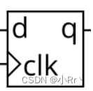
1.D flip-flop
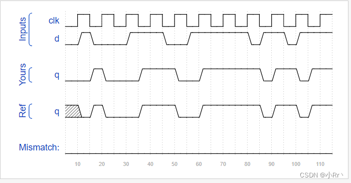
Practice:Create a single D flip-flop.
翻译:创建一个简单的D触发器
Solution(不唯一,仅供参考):
module top_module (
    input clk,    // Clocks are used in sequential circuits
    input d,
    output reg q );//
    always @(posedge clk)begin
        q<=d;
    end
endmodule
Timing Diagram
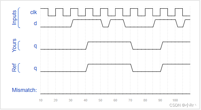
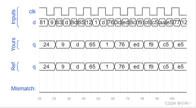
2.D flip-flops
Practice:Create 8 D flip-flops. All DFFs should be triggered by the positive edge of clk.
翻译:创建一个8位的D触发器,所有 DFF 都应由 clk 的上升沿触发。
Solution(不唯一,仅供参考):
module top_module (
    input clk,
    input [7:0] d,
    output reg [7:0]  q
);
    always @(posedge clk)begin
       q<=d;
    end
endmodule
Timing Diagram
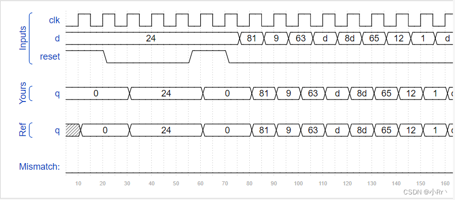
3.DFF with reset
Practice:Create 8 D flip-flops with active high synchronous reset. All DFFs should be triggered by the positive edge of clk.
翻译:实现一个带有复位端的 D 触发器 fdr,即在上题的 8 个 D 触发器基础上,给触发器配上同步复位端口(高电平复位)。
同步置位与复位:
同步置位与复位是指只有在时钟的有效跳变沿时刻置位或复位,信号才能使触发器置位或复位(即使触发器的输出分别转变为逻辑1或0)。因此不要把set和reset信号名列入always块的事件控制表达式。
Solution(不唯一,仅供参考):
module top_module (
    input clk,
    input reset,            // Synchronous reset
    input [7:0] d,
    output reg [7:0] q
);
    always @(posedge clk)begin
        if(reset)begin
           q<=0;
        end
        else begin
           q<=d;
        end
    end
endmodule
Timing Diagram
4.DFF with reset value
Practice:Create 8 D flip-flops with active high synchronous reset. The flip-flops must be reset to 0x34 rather than zero. All DFFs should be triggered by the negative edge of clk.
翻译:创建具有高电平有效同步复位的 8 个 D 触发器,触发器必须重置为 0x34 而不是零。所有的 DFF 应由被时钟下降沿触发。一般管这种复位叫置位,在电路中使用 fds ,带有置位端 s 的触发器实现。
Solution(不唯一,仅供参考):
module top_module (
    input clk,
    input reset,
    input [7:0] d,
    output reg [7:0] q
);
    always @(negedge clk)begin
        if(reset)begin
            q<=8'h34;
        end
        else begin
            q<=d;
        end
    end
endmodule
Timing Diagram

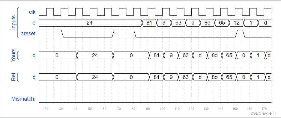
5.DFF with asynchronous reset
Practice:Create 8 D flip-flops with active high asynchronous reset. All DFFs should be triggered by the positive edge of clk.
翻译:创建具有高电平有效异步复位的 8 个 D 触发器。所有 DFF 都应由 clk 的上升沿触发。对应 fdc,它有一个异步复位端 CLR。
同步复位存在一个问题:当同步复位事件发生时,等到下一个时钟上升沿才会得到响应,响应的速度比较慢,异步复位的话可以立即响应。
异步置位与复位:异步置位与复位是与时钟无关的。当异步置位与复位到来时它们立即分别置触发器的输出位1或0,不需要等到时钟沿到来才置位或复位。把它们列入always块的事件控制括号内就能触发always块的执行。
Solution(不唯一,仅供参考):
module top_module (
    input clk,
    input areset,   // active high asynchronous reset
    input [7:0] d,
    output reg [7:0] q
);
    always @(posedge clk or posedge areset)begin
        if(areset)begin
            q<=0;
        end
        else begin
            q<=d;
        end
    end
endmodule
Timing Diagram
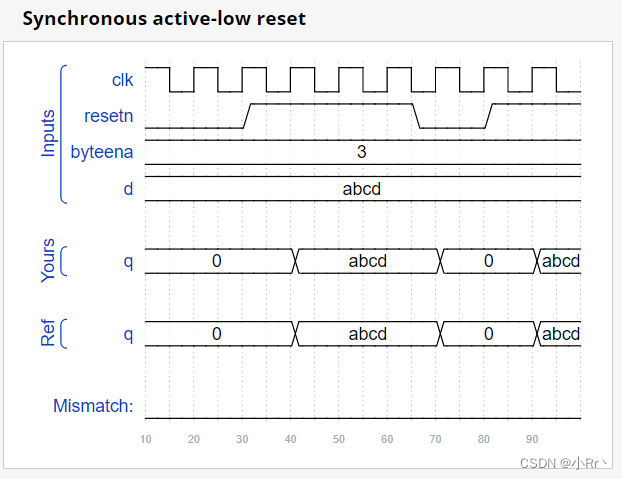
6.DFF with byte enable
Practice:Create 16 D flip-flops. It’s sometimes useful to only modify parts of a group of flip-flops. The byte-enable inputs control whether each byte of the 16 registers should be written to on that cycle. byteena[1] controls the upper byte d[15:8], while byteena[0] controls the lower byte d[7:0].
翻译:本题中需要创建一个 16 路 D 触发器。resetn 为同步低电平有效复位信号。所有的触发器在时钟上升沿被触发。部分情况下,只需要多路触发器中的一部分触发器工作,此时可以通过 ena 使能端进行控制。使能端 ena 信号有效时,触发器在时钟上升沿工作。byteena 使能信号以 byte 为单位管理 8 路触发器在时钟边沿触发与否。byteena [1] 作为 d[15:8] 高位字节的使能端,byteena [0] 则控制 d 的低位字节。
Solution(不唯一,仅供参考):
module top_module (
    input clk,
    input resetn,
    input [1:0] byteena,
    input [15:0] d,
    output reg [15:0] q
);
    always @(posedge clk)begin
        if(!resetn)begin
           q<=0;
        end
        else begin
            if(byteena[0]) q[7:0]<=d[7:0];
            if(byteena[1]) q[15:8]<=d[15:8];
        end
    end
endmodule
Timing Diagram
7.D Latch
Practice:Implement the following circuit:
翻译:实现以下电路
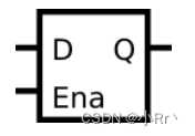
同 D 触发器相比,这个元件没有 clk 端口,取而代之的是 ena 端口,所以这是一个锁存器。D 触发器的触发事件发生于 clk 时钟的边沿,锁存器的触发事件发生于使能端 ena 的电平。
锁存器是一种电平敏感电路,相比之下,触发器属于边沿敏感电路。
Quartus 会 warning 生成了一个锁存器,因为锁存器相比触发器会消耗更多的资源,所以综合器会在推断出锁存器时产生提醒,防止开发者在不想使用锁存器时误产生了锁存器。
Solution(不唯一,仅供参考):
module top_module (
    input d,
    input ena,
    output reg q);
    always @(*) begin
    if(ena)begin
        q<=d;
    end
    end
endmodule
8.DFF
Practice:Implement the following circuit:
翻译:实现以下电路:
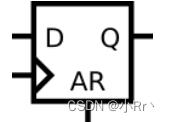
Solution(不唯一,仅供参考):
使用generate语句(具体使用看总结)
module top_module (
    input clk,
    input d,
    input ar,   // asynchronous reset
    output reg q);
    always @(posedge clk or posedge ar)begin
        if(ar) begin
           q<=0;
        end
        else begin
            q<=d;
        end
    end
endmodule
9.DFF
Practice:Implement the following circuit:
翻译:实现以下电路:
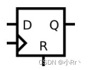
Solution(不唯一,仅供参考):
module top_module (
    input clk,
    input d,
    input r,   // synchronous reset
    output reg q);
    always @(posedge clk)begin
        if(r)begin
           q<=0;
        end
        else begin
          q<=d;
        end
    end
endmodule
10.DFF+gate
Practice:Implement the following circuit:.
翻译:实现以下电路
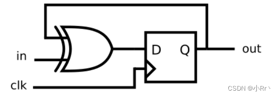
Solution(不唯一,仅供参考):
module top_module (
    input clk,
    input in,
    output reg out);
    always @(posedge clk)begin
        out<= out^in;
    end
endmodule
11.Mux and DFF
Practice:Assume that you want to implement hierarchical Verilog code for this circuit, using three instantiations of a submodule that has a flip-flop and multiplexer in it. Write a Verilog module (containing one flip-flop and multiplexer) named top_module for this submodule.
翻译:考虑以下电路图的时序问题:
假设您要为该电路实现分层 Verilog 代码,使用包含一个触发器和一个多路选择器的子模块的三个实例。为此子模块编写一个名为 top_module 的 Verilog 模块(包含一个触发器和多路复用器)。
module top_module (
	input clk,
	input L,
	input r_in,
	input q_in,
	output reg Q);
    always @(posedge clk)begin
       Q<=L?r_in:q_in;
    end
endmodule
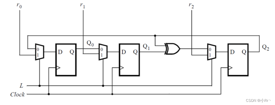
12.Mux and DFF
Practice:Write a Verilog module named top_module for one stage of this circuit, including both the flip-flop and multiplexers.
翻译:考虑如下所示的n位移位寄存器电路:
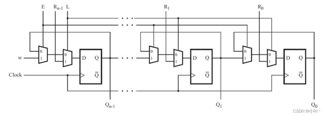
为该电路的一级编写一个名为top_module的Verilog模块,包括触发器和多路复用器。
Solution(不唯一,仅供参考):
module top_module (
    input clk,
    input w, R, E, L,
    output reg Q
);
    always @(posedge clk)begin
        if(L)begin
           Q<= R;
        end
        else begin
            Q<=E?w:Q;
        end
    end
endmodule
13.DFFs and gates
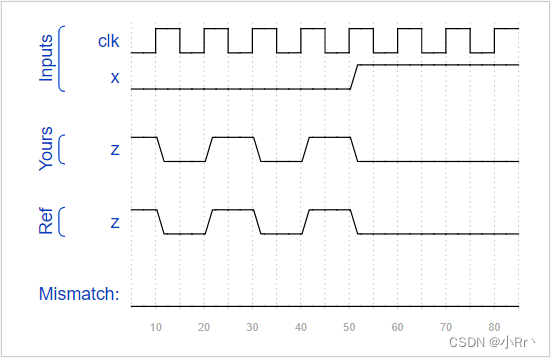
Practice:Given the finite state machine circuit as shown, assume that the D flip-flops are initially reset to zero before the machine begins.Build this circuit.
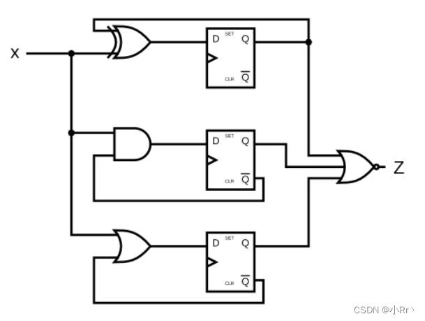
翻译:给定如图所示的有限状态机电路,假设在机器开始之前,D触发器最初被重置为零。建立上图所示电路。
Solution(不唯一,仅供参考):
module top_module (
    input clk,
    input x,
    output  z
);
	reg Q1,Q2,Q3;
    always @(posedge clk)begin
        Q1 <= x^Q1;
        Q2 <= x&(~Q2);
        Q3 <= x|(~Q3);
    end
    assign z = ~(Q1|Q2|Q3);
endmodule
大佬解法
module top_module (
    input clk,
    input x,
    output z
);

    wire w1,w2,w3;
    reg q1=0;
    reg q2=0;
    reg q3=0;
    assign w1 = x^q1;
    assign w2 = x&!q2;
    assign w3 = x|!q3;
    always @(posedge clk) begin
        q1<=w1;
        q2<=w2;
        q3<=w3;
    end
    assign z = !(q1|q2|q3);


endmodule
也可以写作
reg [2:0] q;
always @(posedge clk) begin
    q[2] <= q[2] ^ x;
    q[1] <= x & ~q[1];
    q[0] <= x | ~q[0];
end
assign z = ~(|q);
Timing Diagram
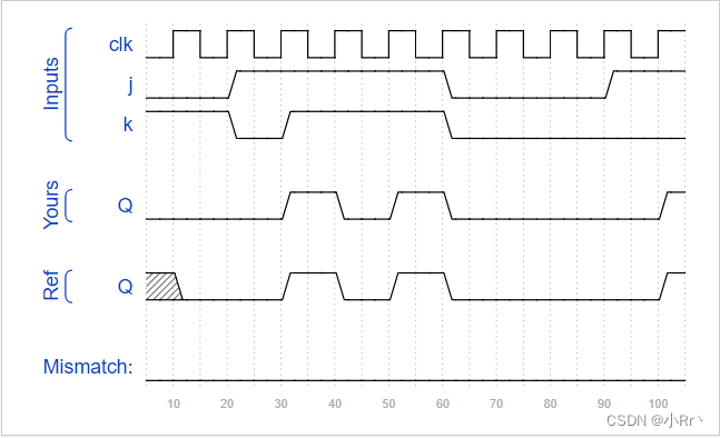
14.Create circuit from truth table
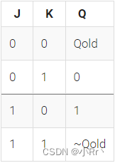
Practice:A JK flip-flop has the below truth table. Implement a JK flip-flop with only a D-type flip-flop and gates. Note: Qold is the output of the D flip-flop before the positive clock edge.
翻译:JK 触发器的真值表如下图所示,仅使用 D 触发器和门电路来实现该 JK 触发器。其中 Qold 是D触发器在时钟上升沿来临之前的输出。
Solution(不唯一,仅供参考):
module top_module (
    input clk,
    input j,
    input k,
    output reg Q);
    always @(posedge clk)begin
        Q<=(j&~Q)|(~k&Q);
    end
endmodule
方法二
module top_module (
    input clk,
    input j,
    input k,
    output reg Q);

    always @(posedge clk) begin
        case ({j,k})
            2'b00: Q<=Q;
            2'b01: Q<=0;
            2'b10: Q<=1;
            2'b11: Q<=!Q;
            default: Q<=0;
        endcase
    end

endmodule
Timing Diagram
15.Detect an edge
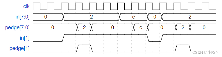
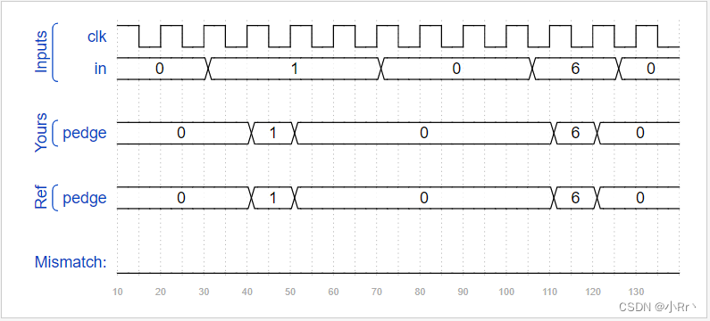
Practice:For each bit in an 8-bit vector, detect when the input signal changes from 0 in one clock cycle to 1 the next (similar to positive edge detection). The output bit should be set the cycle after a 0 to 1 transition occurs.Here are some examples. For clarity, in[1] and pedge[1] are shown separately.
翻译:对于每个 8bit 的变量,检测这些信号什么时候从 0 变为 1(检测上升沿),输出应该在 0 到 1 变化的周期之后才有值。下图展示了输入 in[1] 和输出 pedge[1] 的时序关系图:
关于赋值的延迟:
非阻塞赋值(<=)允许所有的 Verilog 语句同时进行操作,非阻塞赋值是由时钟节拍决定,在时钟上升到来时,执行赋值语句右边,然后将 begin-end 之间的所有赋值语句同时赋值到赋值语句的左边,注意:是 begin—end 之间的所有语句,一起执行,且一个时钟只执行一次。下一周期更新
阻塞赋值(=)在赋值时先计算等号右手方向(RHS)部分的值,这时赋值语句不允许任何别的Verilog语句的干扰,直到现行的赋值完成时刻。从理论上讲,它与后面的赋值语句只有概念上的先后,而无实质上的延迟。可以及时更新
检测上升 / 下降沿:
若采用一个寄存器 Q(rem) 来存储上一个时钟沿的输入值 D(in),当寄存器输出 Q 与输入 D 的值分别为 1、0 时,则检测到下降沿,如下图:
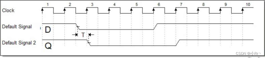
存在问题:输入信号为异步输入,当 D 信号由高变低的时刻发生在趋近时钟上升沿附近时,会导致 D 变化的时刻与 Q 变化的时刻的时间间隔 T 很小,导致边沿检测输出信号脉冲宽度很窄,系统可能会不稳定。
解决方法:将异步输入转化为同步信号,使用一级寄存器对输入信号进行寄存得到同步信号,再通过一级寄存器延迟一个节拍对输入信号的高低电平变化进行判断。通过这种方法可以将下降沿检测输出脉冲保持 1 个采样频率的宽度,使得输出信号十分理想。
module top_module (
    input clk,
    input [7:0] in,
    output reg[7:0] pedge
);
    reg [7:0] in1;
    always @(posedge clk)begin
        in1<=in;
    	pedge<=(in&~in1);
    	//下降沿 (~in&in1)
    end
endmodule
Timing Diagram
16.Detect both edges
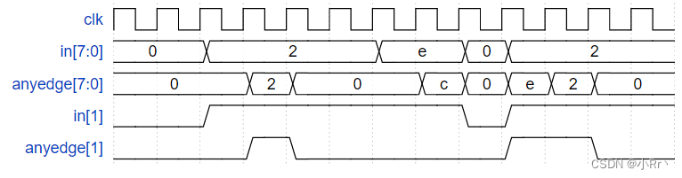
Practice:For each bit in an 8-bit vector, detect when the input signal changes from one clock cycle to the next (detect any edge). The output bit should be set the cycle after a 0 to 1 transition occurs.
Here are some examples. For clarity, in[1] and anyedge[1] are shown separately
翻译:
在一个 8bit 的变量中,从一个周期到另一个周期期间,检测输入信号变化。即上升沿变化或下降沿变化。输出应在 0、1 转换后产生,如下图所示为输入与输出的时序关系:
Solution(不唯一,仅供参考):
module top_module (
    input clk,
    input [7:0] in,
    output reg [7:0] anyedge
);
    reg [7:0] in1;
    always @(posedge clk)begin
       in1<=in;
       anyedge <= in1^in;
    end
endmodule
Timing Diagram
17.Edge capture register
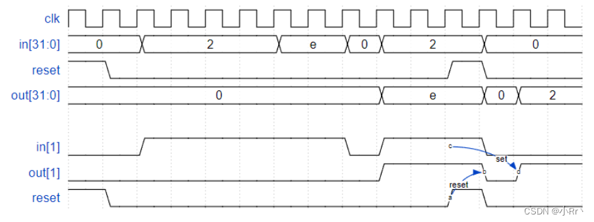
Practice:For each bit in a 32-bit vector, capture when the input signal changes from 1 in one clock cycle to 0 the next. “Capture” means that the output will remain 1 until the register is reset (synchronous reset).
翻译:对于 32bit 中的每一位,捕获输入信号的下降沿。
捕获的意思就是说在寄存器(输出)复位(同步复位)之前,输出一直保持为 ‘1’ 。有个关于捕获的评论很有趣,搬过来分享一下:“检测和捕获的区别在于,捕获只要是发生过一次不管再过多少个时钟周期他的输出还是1,就像是犯罪了,你被捕获了,有一次记录终身有记录,只有当 reset(重启人生)的时候才会变回 0,而检测就是检测这一次的,如果下个时钟周期你不是下降沿了,他就变成 0。”
每一个输出位类似一个 SR 触发器:输出信号从 1 变 0 的转换发生时会保持一个周期(为 1)。当复位为高电平时,输出位应在时钟上升沿复位(为 0)。如果上述两个事件在同时发生,reset 有更高的优先级。在下图所示的最后 4 个周期内,reset 信号比 set 信号早一个周期,所以这里没有冲突发生。
Solution(不唯一,仅供参考):
module top_module (
    input clk,
    input reset,
    input [31:0] in,
    output reg [31:0] out
);
    wire [31:0] a;
    reg [31:0] in1;
    always @(posedge clk)begin
       in1<=in;
    end
    assign a = (in1&~in);
    always @(posedge clk)begin
        if(reset)begin
           out<=0;
        end
        else begin
            for(int i=0;i<32;i++)begin
                if(a[i])begin
                    out[i]<=1;
                end
                else begin
                    out[i]<=out[i];
                end
            end
        end
    end
endmodule
大佬方法:
module top_module (
    input clk,
    input reset,
    input [31:0] in,
    output reg [31:0] out
);

integer i;
reg [31:0] last;
always @(posedge clk) begin
    last <= in;
    if (reset) out <= 0;
    else for (i = 0; i < 32; i = i + 1)
        out[i] <= last[i] & ~in[i] ? 1 : out[i];
end

endmodule
Timing Diagram

18.Dual-edge triggered flip-flop
Practice:Build a circuit that functionally behaves like a dual-edge triggered flip-flop:
翻译:
FPGA 没有一个同时检测双边沿的触发器,而且 always 中的敏感列表也不支持 (posedge clk or negedge clk),设计一个双边沿检测的触发器,时序如下图所示: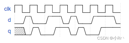
Solution(不唯一,仅供参考):
module top_module (
    input clk,
    input d,
    output q
);

reg q1, q0;
always @(posedge clk)
    q1 <= d;
always @(negedge clk)
    q0 <= d;
assign q = clk ? q1 : q0;

endmodule
大佬写法:
比较合适的方法是设计两个中间变量,分别在时钟上升沿、时钟下降沿进行赋值,最后使用组合逻辑输出。
module top_module (
    input clk,
    input d,
    output q
);
    reg p,n;

    always@(posedge clk)begin
        p <= d ^ n;		//q = p ^ n = d ^ n ^ n = d
    end
    always@(negedge clk)begin
        n <= d ^ p;		//q = p ^ n = p ^ d ^ p = d
    end
    assign q = p ^ n;

endmodule
Timing Diagram
总结
1、 后面几题判断上升沿和下降沿的需要多练习,最后一题要好好理解。
继续加油!!!!!


 1809
1809


 被折叠的 条评论
为什么被折叠?
被折叠的 条评论
为什么被折叠?
 到【灌水乐园】发言


