


ECC纠错算法
原文链接:https://www.cnblogs.com/yysong8020/p/12751533.html
ECC的全称是Error Checking and Correction,是一种用于Nand的差错检测和修正算法。如果操作时序和电路稳定性不存在问题的话,NAND Flash出错的时候一般不会造成整个Block或是Page不能读取或是全部出错,而是整个Page(例如512Bytes)中只有一个或几个bit出错。ECC能纠正1个比特错误和检测2个比特错误,而且计算速度很快,但对1比特以上的错误无法纠正,对2比特以上的错误不保证能检测。
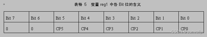
校验码生成算法:ECC校验每次对256字节的数据进行操作,包含列校验和行校验。对每个待校验的Bit位求异或,若结果为0,则表明含有偶数个1;若结果为1,则表明含有奇数个1。列校验规则如表1所示。256字节数据形成256行、8列的矩阵,矩阵每个元素表示一个Bit位。
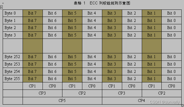
其中CP0 ~ CP5 为六个Bit位,表示Column Parity(列极性),
CP0为第0、2、4、6列的极性,CP1为第1、3、5、7列的极性,
CP2为第0、1、4、5列的极性,CP3为第2、3、6、7列的极性,
CP4为第0、1、2、3列的极性,CP5为第4、5、6、7列的极性。
用公式表示就是:CP0=Bit0^Bit2^Bit4^Bit6, 表示第0列内部256个Bit位异或之后再跟第2列256个Bit位异或,再跟第4列、第6列的每个Bit位异或,这样,CP0其实是256*4=1024个Bit位异或的结果。CP1 ~ CP5 依此类推。
行校验如下图所示
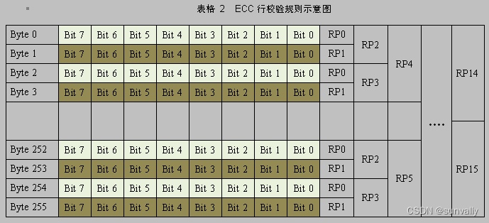
其中RP0 ~ RP15 为十六个Bit位,表示Row Parity(行极性),
RP0为第0、2、4、6、….252、254 个字节的极性
RP1-----1、3、5、7……253、255
RP2----0、1、4、5、8、9……252、253 (处理2个Byte,跳过2个Byte)
RP3---- 2、3、6、7、10、11……254、255 (跳过2个Byte,处理2个Byte)
RP4---- 处理4个Byte,跳过4个Byte;
RP5---- 跳过4个Byte,处理4个Byte;
RP6---- 处理8个Byte,跳过8个Byte
RP7---- 跳过8个Byte,处理8个Byte;
RP8---- 处理16个Byte,跳过16个Byte
RP9---- 跳过16个Byte,处理16个Byte;
RP10----处理32个Byte,跳过32个Byte
RP11----跳过32个Byte,处理32个Byte;
RP12----处理64个Byte,跳过64个Byte
RP13----跳过64个Byte,处理64个Byte;
RP14----处理128个Byte,跳过128个Byte
RP15----跳过128个Byte,处理128个Byte;
可见,RP0 ~ RP15 每个Bit位都是128个字节(也就是128行)即128*8=1024个Bit位求异或的结果。
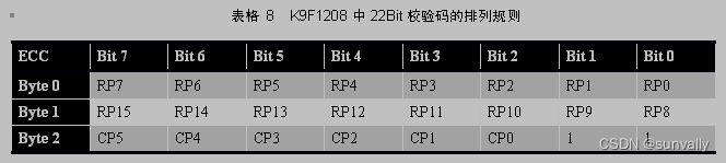
综上所述,对256字节的数据共生成了6个Bit的列校验结果,16个Bit的行校验结果,共22个Bit。在Nand中使用3个字节存放校验结果,多余的两个Bit位置1。存放次序如下表所示:
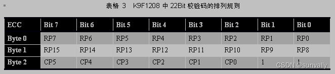
以K9F1208为例,每个Page页包含512字节的数据区和16字节的OOB区。前256字节数据生成3字节ECC校验码,后256字节数据生成3字节ECC校验码,共6字节ECC校验码存放在OOB区中,存放的位置为OOB区的第0、1、2和3、6、7字节。
校验码生成算法的C语言实现
在Linux内核中ECC校验算法所在的文件为drivers/mtd/nand/nand_ecc.c,其实现有新、旧两种,在2.6.27及更早的内核中使用的程序,从2.6.28开始已经不再使用,而换成了效率更高的程序。可以在Documentation/mtd/nand_ecc.txt 文件中找到对新程序的详细介绍。
首先分析一下2.6.27内核中的ECC实现,源代码见:
http://lxr.linux.no/linux+v2.6.27/drivers/mtd/nand/nand_ecc.c
43/*
44 * Pre-calculated 256-way 1 byte column parity
45 */
46static const u_char
nand_ecc_precalc_table[] = {
47   0x00, 0x55, 0x56, 0x03, 0x59, 0x0c, 0x0f, 0x5a, 0x5a, 0x0f, 0x0c, 0x59, 0x03, 0x56, 0x55, 0x00,
48   0x65, 0x30, 0x33, 0x66, 0x3c, 0x69, 0x6a, 0x3f, 0x3f, 0x6a, 0x69, 0x3c, 0x66, 0x33, 0x30, 0x65,
49   0x66, 0x33, 0x30, 0x65, 0x3f, 0x6a, 0x69, 0x3c, 0x3c, 0x69, 0x6a, 0x3f, 0x65, 0x30, 0x33, 0x66,
50   0x03, 0x56, 0x55, 0x00, 0x5a, 0x0f, 0x0c, 0x59, 0x59, 0x0c, 0x0f, 0x5a, 0x00, 0x55, 0x56, 0x03,
51   0x69, 0x3c, 0x3f, 0x6a, 0x30, 0x65, 0x66, 0x33, 0x33, 0x66, 0x65, 0x30, 0x6a, 0x3f, 0x3c, 0x69,
52   0x0c, 0x59, 0x5a, 0x0f, 0x55, 0x00, 0x03, 0x56, 0x56, 0x03, 0x00, 0x55, 0x0f, 0x5a, 0x59, 0x0c,
53   0x0f, 0x5a, 0x59, 0x0c, 0x56, 0x03, 0x00, 0x55, 0x55, 0x00, 0x03, 0x56, 0x0c, 0x59, 0x5a, 0x0f,
54   0x6a, 0x3f, 0x3c, 0x69, 0x33, 0x66, 0x65, 0x30, 0x30, 0x65, 0x66, 0x33, 0x69, 0x3c, 0x3f, 0x6a,
55   0x6a, 0x3f, 0x3c, 0x69, 0x33, 0x66, 0x65, 0x30, 0x30, 0x65, 0x66, 0x33, 0x69, 0x3c, 0x3f, 0x6a,
56   0x0f, 0x5a, 0x59, 0x0c, 0x56, 0x03, 0x00, 0x55, 0x55, 0x00, 0x03, 0x56, 0x0c, 0x59, 0x5a, 0x0f,
57   0x0c, 0x59, 0x5a, 0x0f, 0x55, 0x00, 0x03, 0x56, 0x56, 0x03, 0x00, 0x55, 0x0f, 0x5a, 0x59, 0x0c,
58   0x69, 0x3c, 0x3f, 0x6a, 0x30, 0x65, 0x66, 0x33, 0x33, 0x66, 0x65, 0x30, 0x6a, 0x3f, 0x3c, 0x69,
59   0x03, 0x56, 0x55, 0x00, 0x5a, 0x0f, 0x0c, 0x59, 0x59, 0x0c, 0x0f, 0x5a, 0x00, 0x55, 0x56, 0x03,
60   0x66, 0x33, 0x30, 0x65, 0x3f, 0x6a, 0x69, 0x3c, 0x3c, 0x69, 0x6a, 0x3f, 0x65, 0x30, 0x33, 0x66,
61   0x65, 0x30, 0x33, 0x66, 0x3c, 0x69, 0x6a, 0x3f, 0x3f, 0x6a, 0x69, 0x3c, 0x66, 0x33, 0x30, 0x65,
62   0x00, 0x55, 0x56, 0x03, 0x59, 0x0c, 0x0f, 0x5a, 0x5a, 0x0f, 0x0c, 0x59, 0x03, 0x56, 0x55, 0x00
63};
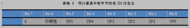
为了加快计算速度,程序中使用了一个预先计算好的列极性表。这个表中每一个元素都是unsigned char类型,表示8位二进制数。表中8位二进制数每位的含义:
这个表的意思是:对0~255这256个数,计算并存储每个数的列校验值和行校验值,以数作数组下标。比如 nand_ecc_precalc_table[ 13 ] 存储13的列校验值和行校验值,13的二进制表示为 00001101, 其
CP0 = Bit0^Bit2^Bit4^Bit6 = 0;
CP1 = Bit1^Bit3^Bit5^Bit7 = 1;
CP2 = Bit0^Bit1^Bit4^Bit5 = 1;
CP3 = Bit2^Bit3^Bit6^Bit7 = 0;
CP4 = Bit0^Bit1^Bit2^Bit3 = 1;
CP5 = Bit4^Bit5^Bit6^Bit7 = 0;
其行极性RP = Bit0^Bit1^Bit2^Bit3^Bit4^Bit5^Bit6^Bit7 = 1;
则nand_ecc_precalc_table[ 13 ] 处存储的值应该是 0101 0110,即0x56.
注意,数组nand_ecc_precalc_table的下标其实是我们要校验的一个字节数据。
理解了这个表的含义,也就很容易写个程序生成这个表了。程序见附件中的 MakeEccTable.c文件。
有了这个表,对单字节数据dat,可以直接查表 nand_ecc_precalc_table[ dat ] 得到 dat的行校验值和列校验值。 但是ECC实际要校验的是256字节的数据,需要进行256次查表,对得到的256个查表结果进行按位异或,最终结果的 Bit0 ~ Bit5 即是256字节数据的 CP0 ~ CP5.
/* Build up column parity */
for(i = 0; i < 256; i++) {
/* Get CP0 - CP5 from table */
idx = nand_ecc_precalc_table[*dat++];
reg1 ^= (idx & 0x3f);
//这里省略了一些,后面会介绍
}
reg1
在这里,计算列极性的过程其实是先在一个字节数据的内部计算CP0 ~ CP5, 每个字节都计算完后再与其它字节的计算结果求异或。而表1中是先对一列Bit0求异或,再去异或一列Bit2。 这两种只是计算顺序不同,结果是一致的。 因为异或运算的顺序是可交换的。
行极性的计算要复杂一些。
nand_ecc_precalc_table[] 表中的 Bit6 已经保存了每个单字节数的行极性值。对于待校验的256字节数据,分别查表,如果其行极性为1,则记录该数据所在的行索引(也就是for循环的i值),这里的行索引是很重要的,因为RP0 ~ RP15 的计算都是跟行索引紧密相关的,如RP0只计算偶数行,RP1只计算奇数行,等等。
当往NAND Flash的page中写入数据的时候,每256字节我们生成一个ECC校验和,称之为原ECC校验和,保存到PAGE的OOB(out-of-band)数据区中。
当从NAND Flash中读取数据的时候,每256字节我们生成一个ECC校验和,称之为新ECC校验和。
将从OOB区中读出的原ECC校验和新ECC校验和按位异或,若结果为0,则表示不存在错(或是出错了,ECC无法检测的错误);若3个字节异或结果中存在11个比特位为1,表示存在一个比特错误,且可纠正;若3个字节异或结果中只存在1个比特位为1,表示 OOB区出错;其他情况均表示出现了无法纠正的错误。
假设ecc_code_raw[3] 保存原始的ECC校验码,ecc_code_new[3] 保存新计算出的ECC校验码,其格式如下表所示:
对ecc_code_raw[3] 和 ecc_code_new[3] 按位异或,得到的结果三个字节分别保存在s0,s1,s2中,如果s0s1s2中共有11个Bit位为1,则表示出现了一个比特位错误,可以修正。定位出错的比特位的方法是,先确定行地址(即哪个字节出错),再确定列地址(即该字节中的哪一个Bit位出错)。
确定行地址的方法是:
设行地址为unsigned char byteoffs,抽取s1中的Bit7,Bit5,Bit3,Bit1,作为 byteoffs的高四位, 抽取s0中的Bit7,Bit5,Bit3,Bit1 作为byteoffs的低四位, 则byteoffs的值就表示出错字节的行地址(范围为0 ~ 255)。
确定列地址的方法是:
抽取s2中的Bit7,Bit5,Bit3 作为 bitnum 的低三位,bitnum其余位置0,则bitnum的表示出错Bit位的列地址 (范围为0 ~ 7)。
参考博客的最后给举出了一个示例,可以帮助理解。
TN-29-63 Error Correction Code (ECC) in SLC NAND ECC for Memory Devices
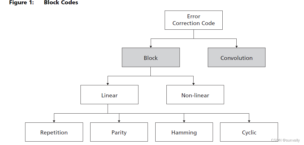
There are two basic types of ECC (see Figure 1 on page 2):
-
Block codes: These codes are referred to as “n” and “k” codes. A block of k data bits is
encoded to become a block of n bits called a code word. In block codes, code words
do not have any dependency on previously encoded messages. NAND Flash memory
devices typically use block codes. -
Convolution codes: These codes produce code words that depend on both the data
message and a given number of previously encoded messages. The encoder changes
state with every message processed. Typically, the length of the code word constant.
Block Codes
As previously described, block codes are referred to as n and k codes. A block of k data
bits is encoded to become a block of n bits called a code word. A block code takes k data
bits and computes (n - k) parity bits from the code generator matrix.
The block code family can be divided in linear and non-linear codes, as shown in
Figure 1. Either type can be systematic. Most block codes are systematic in that the data
bits remain unchanged, with the parity bits attached either to the front or to the back of
the data sequence.
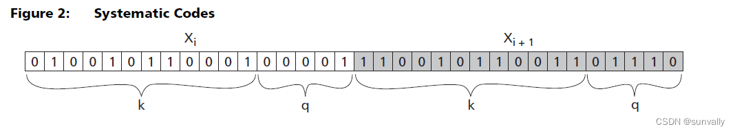
Systematic Codes
In systematic (linear or non-linear) block codes, each code word includes the exact data
bits from the original message of length k, either followed or preceded by a separate
group of check bits of length q (see Figure 2). The ratio k / (k + q) is called the code rate.
Improving the quality of a code often means increasing its redundancy and, thus,
reducing the code rate.
The set of all possible code words is called the code space.
Linear Codes
In linear block codes, every linear combination of valid code words (such as a binary
sum) produces another valid code word. In all linear codes, the code words are longer
than the data words on which they are based.
Micron NAND Flash memory devices use cyclic and Hamming linear codes.
Cyclic Codes
Cyclic codes are a type of linear code where every cyclic shift by a valid code word also
yields a valid code word.
Hamming Codes
Hamming codes are the most widely used linear block codes. Typically, a Hamming code
is defined as (2n - 1, 2n - n - 1), where:
- n is equal to the number of overhead bits.
- 2n - 1 is equal to the block size.
- 2n - n - 1 is equal to the number of data bits in the block.
All Hamming codes can detect three errors and one correct one. Common Hamming
code sizes are (7, 4), (15,11), and (31, 26). All have the same Hamming distance.
The Hamming distance and the Hamming weight are useful in encoding. When the
Hamming distance is known, the capability of a code to detect and correct errors can be
determined.
Hamming Distance
In continuous variables, distances are measured using euclidean concepts, such as
lengths, angles, and vectors.
In binary encoding, the distance between two binary words is called the Hamming
distance. It is the number of discrepancies between two binary sequences of the same
size. The Hamming distance measures how different the binary objects are. For example,
the Hamming distance between sequences 0011001 and 1010100 is 4.
The Hamming code minimum distance dmin is the minimum distance between all code
word pairs.
Hamming Weight
The Hamming weight of a code scheme is the maximum number of 1s among valid code
words.
Error Detection Capability
For a code where dmin is the Hamming distance between code words, the maximum
number of error bits that can be detected is t = dmin - 1. This means that 1-bit and 2-bit
errors can be detected for a code where dmin = 3.
Error Correction Capability
For a code where dmin is the Hamming distance between code words, the maximum
number of error bits that can be corrected is t = (dmin – 1) § 2. This means that 1-bit
errors can be corrected for a code where dmin = 3.
ECC for Memory Devices
Common error correction capabilities for memory devices are:
- Single error correction (SEC) Hamming codes
- Single error correction/double error detection (SEC-DED) Hsiao codes
- Single error correction/double error detection/single byte error detection (SEC-DEDSBD) Reddy codes
- Single byte error correction/double byte error detection (SBC-DBD) finite field-based codes
- Double error correction/triple error detection (DEC-TED) Bose-Chaudhuri-Hocquenghem codes
ECC Generation
According to the Hamming ECC principle, a 22-bit ECC is generated to perform a 1-bit
correction per 256 bytes. The Hamming ECC can be applied to data sizes of 1 byte, 8
bytes, 16 bytes, and so on.
For 528-byte/264-word page NAND devices, a Hamming ECC principle can be used that
generates a 24-bit ECC per 512 bytes to perform a 2-bit detection and a 1-bit correction.
For 2112-byte/1056-word page NAND devices, the calculation can be done per 512
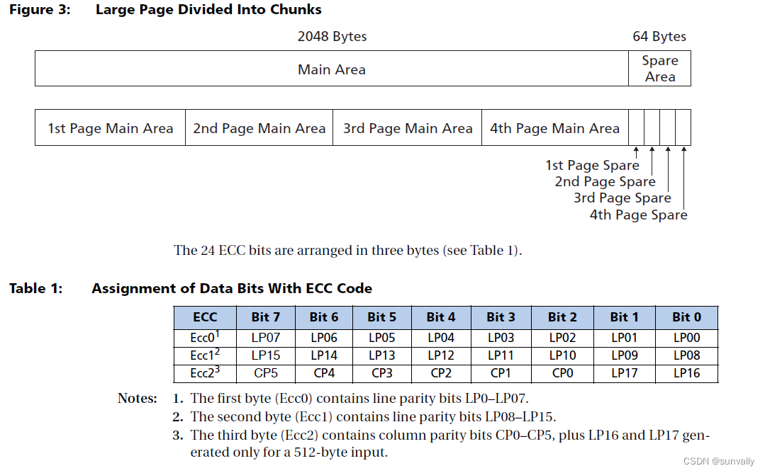
bytes, which means a 24-bit ECC per 4096 bits (exactly 3 bytes per 512 bytes). 2112 byte
pages are divided into 512 byte (+ 16 byte spare) chunks (see Figure 3).

ECC Generation Pseudo Code
The following pseudo code implements the parity generation shown in Figure 4 on page 5.
For i = 1 to 2561
begin
if (i & 0x01)
LP1=bit7 ⊕1 bit6 ⊕ bit5 ⊕ bit4 ⊕ bit3 ⊕ bit2 ⊕ bit1 ⊕ bit0 ⊕ LP1;
else
LP0=bit7 ⊕ bit6 ⊕ bit5 ⊕ bit4 ⊕ bit3 ⊕ bit2 ⊕ bit1 ⊕ bit0
⊕ LP1;
if (i & 0x02)
LP3=bit7 ⊕ bit6 ⊕ bit5 ⊕ bit4 ⊕ bit3 ⊕ bit2 ⊕ bit1 ⊕ bit0
⊕ LP3;
else
LP2=bit7 ⊕ bit6 ⊕ bit5 ⊕ bit4 ⊕ bit3 ⊕ bit2 ⊕ bit1 ⊕ bit0
⊕ LP2;
if (i & 0x04)
LP5=bit7 ⊕ bit6 ⊕ bit5 ⊕ bit4 ⊕ bit3 ⊕ bit2 ⊕ bit1 ⊕ bit0
⊕ LP5;
else
LP4=bit7 ⊕ bit6 ⊕ bit5 ⊕ bit4 ⊕ bit3 ⊕ bit2 ⊕ bit1 ⊕ bit0
⊕ LP4;
if (i & 0x08)
LP7=bit7 ⊕ bit6 ⊕ bit5 ⊕ bit4 ⊕ bit3 ⊕ bit2 ⊕ bit1 ⊕ bit0
⊕ LP7;
else
LP6=bit7 ⊕ bit6 ⊕ bit5 ⊕ bit4 ⊕ bit3 ⊕ bit2 ⊕ bit1 ⊕ bit0
⊕ LP6;
if (i & 0x10)
LP9=bit7 ⊕ bit6 ⊕ bit5 ⊕ bit4 ⊕ bit3 ⊕ bit2 ⊕ bit1 ⊕ bit0
⊕ LP9;
else
LP8=bit7 ⊕ bit6 ⊕ bit5 ⊕ bit4 ⊕ bit3 ⊕ bit2 ⊕ bit1 ⊕ bit0
⊕ LP8;
if (i & 0x20)
LP11=bit7 ⊕ bit6 ⊕ bit5 ⊕ bit4 ⊕ bit3 ⊕ bit2 ⊕ bit1 ⊕ bit0 ⊕ LP11;
else
LP10=bit7 ⊕ bit6 ⊕ bit5 ⊕ bit4 ⊕ bit3 ⊕ bit2 ⊕ bit1 ⊕ bit0 ⊕
LP10;
if (i & 0x40)
LP13=bit7 ⊕ bit6 ⊕ bit5 ⊕ bit4 ⊕ bit3 ⊕ bit2 ⊕ bit1 ⊕ bit0 ⊕ LP13;
else
LP12=bit7 ⊕ bit6 ⊕ bit5 ⊕ bit4 ⊕ bit3 ⊕ bit2 ⊕ bit1 ⊕ bit0
⊕ LP12; if (i & 0x80)
LP15=bit7 ⊕ bit6 ⊕ bit5 ⊕ bit4 ⊕ bit3 ⊕ bit2 ⊕ bit1 ⊕ bit0 ⊕ LP15;
else
LP14=bit7 ⊕ bit6 ⊕ bit5 ⊕ bit4 ⊕ bit3 ⊕ bit2 ⊕ bit1 ⊕ bit0 ⊕ LP14;
if(i & A0)
LP17=bit7 (Xor) bit6 (Xor) bit5 (Xor) bit4 (Xor) bit3 (Xor) bit2
(Xor) bit1 (Xor) bit0 (Xor) LP17
else
LP16=bit7 (Xor) bit6 (Xor) bit5 (Xor) bit4 (Xor) bit3 (Xor) bit2
(Xor) bit1 (Xor) bit0 (Xor) LP163
CP0 = bit6 ⊕ bit4 ⊕ bit2 ⊕ bit0 ⊕ CP0;
CP1 = bit7 ⊕ bit5 ⊕ bit3 ⊕ bit1 ⊕ CP1;
CP2 = bit5 ⊕ bit4 ⊕ bit1 ⊕ bit0 ⊕ CP2;
CP3 = bit7 ⊕ bit6 ⊕ bit3 ⊕ bit2 ⊕ CP3
CP4 = bit3 ⊕ bit2 ⊕ bit1 ⊕ bit0 ⊕ CP4
CP5 = bit7 ⊕ bit6 ⊕ bit5 ⊕ bit4 ⊕ CP5
end
Notes:
- For 512-byte inputs, the “i” range is from 1–512 bytes.
- “⊕” indicates a bitwise XOR operation.
- The last control “if(i & A0)” is executed only in the case of 512-byte inputs.
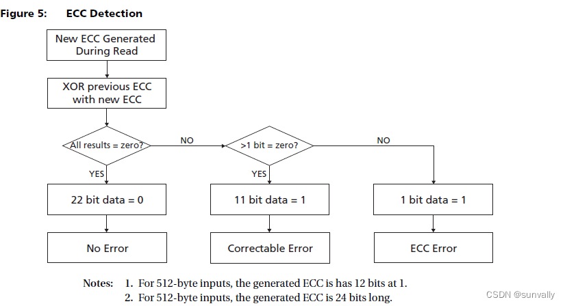
ECC Detection and Correction
ECC can detect the following:
• No error: The result of XOR is 0.
• Correctable error: The result of XOR is a code with 11 bits at 1. For 512-byte inputs,
the generated ECC has 12 bits at 1.
• ECC error: The result of XOR has only 1 bit at 1. This means that the error is in the ECC
area.
• Non-correctable error: The result of XOR provides all other results.
When the main area has a 1-bit error, each parity pair (for example, LP0 and LP1) is 1 and
0 or 0 and 1.
The fail bit address offset can be obtained by retrieving the following bits from the result
of XOR:
• Byte address = (LP17,LP15,LP13,LP11,LP9,LP7,LP5,LP3,LP1). For 512-byte inputs, the
resulting byte address is LP17.
• Bit address = (CP5, CP3,CP1)
When the NAND devices has more than two bit errors, the data cannot be corrected.
ECC Detection and Correction Pseudo Code
% Detect and correct a 1 bit error for 256 byte block int ecc_check (data, stored_ecc, new_ecc)
begin
% Basic Error Detection phase
ecc_xor[0] = new_ecc[0] ⊕ stored_ecc[0];
ecc_xor[1] = new_ecc[1] ⊕ stored_ecc[1];
ecc_xor[2] = new_ecc[2] ⊕ stored_ecc[2];
if ((ecc_xor[0] or ecc_xor[1] or ecc_xor[2]) == 0)
begin
return 0; % No errors
end
else
begin
% Counts the bit number
bit_count = BitCount(ecc_xor);
if (bit_count == 11)
begin
% Set the bit address
bit_address = (ecc_xor[2] >> 3) and 0x01 or
(ecc_xor[2] >> 4) and 0x02 or
(ecc_xor[2] >> 5) and 0x04;
byte_address = (ecc_xor[0] >> 1) and 0x01 or
(ecc_xor[0] >> 2) and 0x02 or
(ecc_xor[0] >> 3) and 0x04 or
(ecc_xor[0] >> 4) and 0x08 or
(ecc_xor[1] << 3) and 0x10 or
(ecc_xor[1] << 2) and 0x20 or
(ecc_xor[1] << 1) and 0x40 or
(ecc_xor[1] and 0x80);
% Correct bit error in the data
data[byte_address]=data[byte_address]⊕(0x01<<bit_address);
return 1;
end
else if (bit_count == 1)
begin
% ECC Code Error Correction
stored_ecc[0] = new_ecc[0];
stored_ecc[1] = new_ecc[1];
stored_ecc[2] = new_ecc[2];
return 2;
end
else
begin
% Uncorrectable Error
return -1;
end
end
end
Note: “⊕” indicates bitwise XOR.


 7531
7531

 被折叠的 条评论
为什么被折叠?
被折叠的 条评论
为什么被折叠?
 到【灌水乐园】发言


