


本文主要介绍组合逻辑,组合逻辑电路的特点是任意时刻的输出仅仅取决于输入信号,输入 信号变化,输出立即变化,不依赖于时钟。
1、与门
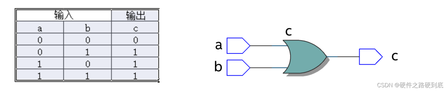
在 verilog 中以“&”表示按位与,如 c=a&b,真值表如下,在 a 和 b 都等于 1 时结果才为 1, RTL 表示如右图。

代码实现如下:
module top(a, b, c) ;
input a ;
input b ;
output c ;
assign c = a & b ;
endmodule
激励文件如下:
`timescale 1 ns/1 ns
module top_tb() ;
reg a ;
reg b ;
wire c ;
initial
begin
 a = 0 ;
 b = 0 ;
 forever
 begin
 #({$random}%100)
 a = ~a ;
 #({$random}%100)
 b = ~b ;
 end
end
top t0(.a(a), .b(b),.c(c)) ;
endmodule
仿真结果如下:

如果 a 和 b 的位宽大于 1,例如定义 input [3:0] a, input [3:0]b,那么 a&b 则指 a 与 b 的对应位 相与。如 a[0]&b[0],a[1]&b[1]。
2、或门
在 verilog 中以“|”表示按位或,如 c = a|b , 真值表如下,在 a 和 b 都为 0 时结果才为 0。
代码实现如下:
module top(a, b, c) ;
input a ;
input b ;
output c ;
assign c = a | b ;
endmodule
激励文件如下:
`timescale 1 ns/1 ns
module top_tb() ;
reg a ;
reg b ;
wire c ;
initial
begin
 a = 0 ;
 b = 0 ;
 forever
 begin
 #({$random}%100)
 a = ~a ;
 #({$random}%100)
 b = ~b ;
 end
end
top t0(.a(a), .b(b),.c(c)) ;
endmodule
仿真结果如下:

同理,位宽大于 1,则是按位或。
3、非门
在 verilog 中以“~”表示按位取反,如 b=~a,真值表如下,b 等于 a 的相反数。

代码实现如下:
module top(a, b) ;
input a ;
output b ;
assign b = ~a ;
endmodule
激励文件如下:
`timescale 1 ns/1 ns
module top_tb() ;
reg a ;
wire b ;
initial
begin
 a = 0 ;
 forever
 begin
 #({$random}%100)
 a = ~a ;
 end
end
top t0(.a(a), .b(b)) ;
endmodule
仿真结果如如下:

4、异或
在 verilog 中以“^”表示异或,如 c= a^b ,真值表如下,当 a 和 b 相同时,输出为 0。

代码实现如下:
module top(a, b, c) ;
input a ;
input b ;
output c ;
assign c = a ^ b ;
endmodule
激励文件如下:
`timescale 1 ns/1 ns
module top_tb() ;
reg a ;
reg b ;
wire c ;
initial
begin
 a = 0 ;
 b = 0 ;
 forever
 begin
 #({$random}%100)
 a = ~a ;
 #({$random}%100)
 b = ~b ;
 end
end
top t0(.a(a), .b(b),.c(c)) ;
endmodule
仿真结果如下:

5、比较器
在 verilog 中以大于“>”,等于”==”,小于”<”,大于等于”>=”,小于等于”<=”,不等于”!=”表示,以大于举例,如 c= a > b ;表示如果 a 大于 b,那么 c 的值就为 1,否则为 0。真值表如下:

代码实现如下:
module top(a, b, c) ;
input a ;
input b ;
output c ;
assign c = a > b ;
endmodule
激励文件如下:
`timescale 1 ns/1 ns
module top_tb() ;
reg a ;
reg b ;
wire c ;
initial
begin
 a = 0 ;
 b = 0 ;
 forever
 begin
 #({$random}%100)
 a = ~a ;
 #({$random}%100)
 b = ~b ;
 end
end
top t0(.a(a), .b(b),.c(c)) ;
endmodule
仿真结果如下:

6、半加器
半加器和全加器是算术运算电路中的基本单元,由于半加器不考虑从低位来的进位,所以称 之为半加器,sum 表示相加结果,count 表示进位,真值表可表示如下:

可根据真值表写出代码如下:
module top(a, b, sum, count) ;
input a ;
input b ;
output sum ;
output count ;
assign sum = a ^ b ;
assign count = a & b ;
endmodule
激励文件如下:
`timescale 1 ns/1 ns
module top_tb() ;
reg a ;
reg b ;
wire sum ;
wire count ;
initial
begin
 a = 0 ;
 b = 0 ;
 forever
 begin
 #({$random}%100)
 a = ~a ;
 #({$random}%100)
 b = ~b ;
 end
 end
top t0(.a(a), .b(b),
.sum(sum), .count(count)) ;
endmodule
仿真结果如下:

7、全加器
而全加器需要加上低位来的进位信号 cin,真值表如下:

代码如下:
module top(cin, a, b, sum, count) ;
input cin ;
input a ;
input b ;
output sum ;
output count ;
assign {count,sum} = a + b + cin ;
endmodule
激励文件如下:
`timescale 1 ns/1 ns
module top_tb() ;
reg a ;
reg b ;
reg cin ;
wire sum ;
wire count ;
initial
begin
 a = 0 ;
 b = 0 ;
 cin = 0 ;
 forever
 begin
 #({$random}%100)
 a = ~a ;
 #({$random}%100)
b = ~b ;
#({$random}%100)
 cin = ~cin ;
 end
end
top t0(.cin(cin),.a(a), .b(b),
.sum(sum), .count(count)) ;
endmodule
仿真结果如下:

8、乘法器
乘法的表示也很简单,利用”*”即可,如 a*b,举例代码如下:
module top(a, b, c) ;
input [1:0] a ;
input [1:0] b ;
output [3:0] c ;
assign c = a * b ;
endmodule
激励文件如下:
`timescale 1 ns/1 ns
module top_tb() ;
reg [1:0] a ;
reg [1:0] b ;
wire [3:0] c ;
initial
begin
 a = 0 ;
 b = 0 ;
 forever
 begin
 #({$random}%100)
 a = ~a ;
 #({$random}%100)
 b = ~b ;
 end
end
top t0(.a(a), .b(b),.c(c)) ;
endmodule
仿真结果如下:

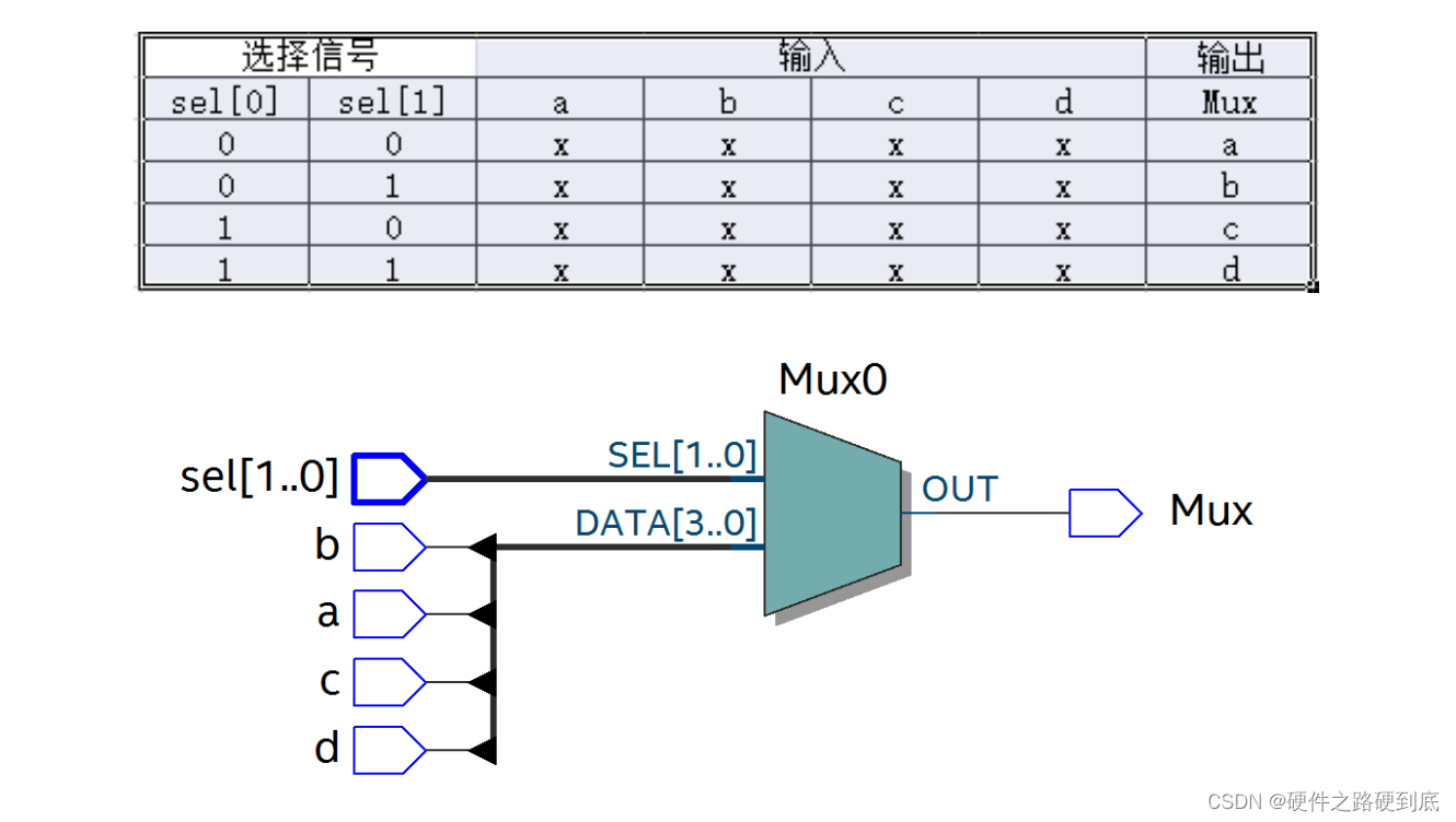
9、数据选择器
在 verilog 中经常会用到数据选择器,通过选择信号,选择不同的输入信号输出到输出端,如 下图真值表,四选一数据选择器,sel[1:0]为选择信号,a,b,c,d 为输入信号,Mux 为输出信号。
代码如下:
module top(a, b, c, d, sel, Mux) ;
input a ;
input b ;
input c ;
input d ;
input [1:0] sel ;
output reg Mux ;
always @(sel or a or b or c or d)
begin
 case(sel)
 2'b00 : Mux = a ;
 2'b01 : Mux = b ;
 2'b10 : Mux = c ;
 2'b11 : Mux = d ;
 endcase
end

endmodule
激励文件如下:
`timescale 1 ns/1 ns
module top_tb() ;
reg a ;
reg b ;
reg c ;
reg d ;
reg [1:0] sel ;
wire Mux ;
initial
begin
 a = 0 ;
 b = 0 ;
 c = 0 ;
 d = 0 ;
 forever
 begin
 #({$random}%100)
 a = {$random}%3 ;
 #({$random}%100)
 b = {$random}%3 ;
 #({$random}%100)
 c = {$random}%3 ;
 #({$random}%100)
 d = {$random}%3 ;
 end
 end
initial
begin
 sel = 2'b00 ;
 #2000 sel = 2'b01 ;
 #2000 sel = 2'b10 ;
 #2000 sel = 2'b11 ;
end
top
t0(.a(a), .b(b),.c(c),.d(d), .sel(sel),
.Mux(Mux)) ;
endmodule
仿真结果如下

10、3-8译码器
3-8 译码器是一个很常用的器件,其真值表如下所示,根据 A2,A1,A0 的值,得出不同的结果。


代码如下:
module top(addr, decoder) ;
input [2:0] addr ;
output reg [7:0] decoder ;
always @(addr)
begin
 case(addr)
 3'b000 : decoder = 8'b1111_1110 ;
 3'b001 : decoder = 8'b1111_1101 ;
 3'b010 : decoder = 8'b1111_1011 ;
 3'b011 : decoder = 8'b1111_0111 ;
 3'b100 : decoder = 8'b1110_1111 ;
 3'b101 : decoder = 8'b1101_1111 ;
 3'b110 : decoder = 8'b1011_1111 ;
 3'b111 : decoder = 8'b0111_1111 ;
 endcase
end

endmodule
激励文件如下:
`timescale 1 ns/1 ns
module top_tb() ;
reg [2:0] addr ;
wire [7:0] decoder ;
initial
begin
 addr = 3'b000 ;
 #2000 addr = 3'b001 ;
 #2000 addr = 3'b010 ;
 #2000 addr = 3'b011 ;
 #2000 addr = 3'b100 ;
 #2000 addr = 3'b101 ;
 #2000 addr = 3'b110 ;
 #2000 addr = 3'b111 ;
end
top
t0(.addr(addr),.decoder(decoder)) ;
endmodule
仿真结果如下:

11、三态门
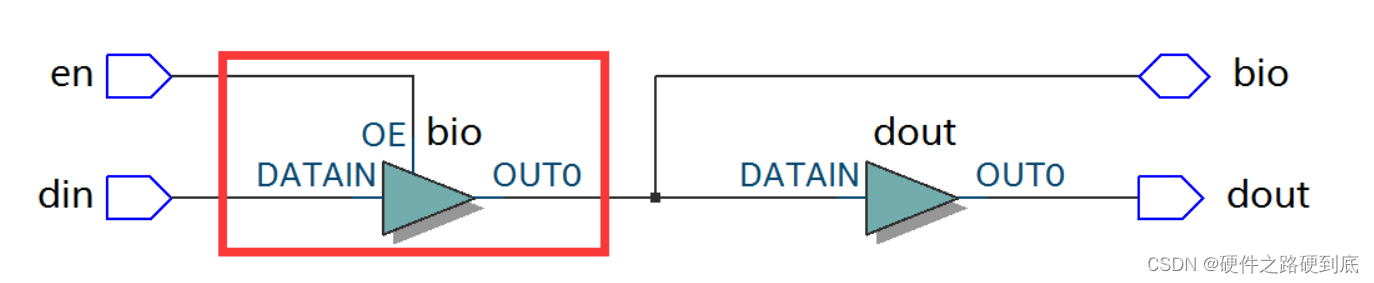
在 FPGA 使用中,经常会用到双向 IO,需要用到三态门,如 bio = en? din: 1’bz ;其中 en 为使能 信号,用于打开关闭三态门,下面的 RTL 图即是实现了双向 IO,可参考代码。激励文件实现两个 双向 IO 的对接。
代码:
module top(en, din, dout, bio) ;
input din ;
input en ;
output dout ;
inout bio ;
assign bio = en? din : 1'bz ;
assign dout = bio ;

endmodule
激励:
`timescale 1 ns/1 ns
module top_tb() ;
reg en0 ;
reg din0 ;
wire dout0 ;
reg en1 ;
reg din1 ;
wire dout1 ;
wire bio ;
initial
begin
 din0 = 0 ;
 din1 = 0 ;
 forever
 begin
 #({$random}%100)
 din0 = ~din0 ;
 #({$random}%100)
din1 = ~din1 ;
 end
end
initial
begin
 en0 = 0 ;
 en1 = 1 ;
 #100000
 en0 = 1 ;
 en1 = 0 ;
end
top
t0(.en(en0),.din(din0),.dout(dout0),.bi
o(bio)) ;
top
t1(.en(en1),.din(din1),.dout(dout1),.bi
o(bio)) ;
endmodule
激励文件结构如下图

仿真结果如下,en0 为 0,en1 为 1 时,1 通道打开,双向 IO bio 就等于 1 通道的 din1,1 通 道向外发送数据,0 通道接收数据,dout0 等于 bio;当 en0 为 1,en1 为 0 时,0 通道打开,双向 IO bio 就等于 0 通道的 din0,0 通道向外发送数据,1 通道接收数据,dout1 等于 bio


 1947
1947


 被折叠的 条评论
为什么被折叠?
被折叠的 条评论
为什么被折叠?
 到【灌水乐园】发言


