


AXI_Full实验
什么是AXI
总线、接口和协议,这三个词常常被联系在一起,但是我们要明白他们的区别。总线是一组传输通道,是各种逻辑器件构成的传输数据的通道,一般由数据线、地址线、控制线等构成。接口是一种连接标准,又常常被称之为物理接口。协议是传输数据的规则。
三种AXI总线
在数字电路中只能传输二进制数0和1,因此需要一组信号才能高速的传输信息,这一组信号就成了接口。AXI(Advanced eXtensible Interface)是一种总协议。AXI4包含3种类型的接口(或者说ZYNQ的三种AXI总线)。
- AXI4:(For high-performance memory-mapped requirements),主要面向高性能地址映射通信的需求,是面向地址映射的接口,允许最大256轮的数据突发传输。
- AXI4-Lite:(For simple, low-throughput memory-mapped communication),是一个轻量级的地址映射单次传输接口,占用很少的逻辑单元。适用于吞吐量较小的地址映射通信总线。
- AXI4-Stream:(For high-speed streaming data.)面向高速流数据传输;去掉了地址项,允许无限制的数据突发传输规模。
NOTE:AXI4:面向地址映射的接口,在单地址传输的情况下最大允许256个时钟周期的数据突发长度;AXI4-Lite:一个轻量级的地址映射单次传输接口,占用较少的资源;AXI4-Stream:去掉了地址传输的功能,允许无限制的数据突发传输,无需考虑地址映射。
在这里我们首先解释一下存储映射(Meamory Map)这一概念。如果一个协议是存储映射的,那么主机所发出的会话(无论读或写)就会标明一个地址。这个地址对应于系统存储空间中的一个地址,表明是针对该存储空间的读写操作。
AXI4 协议支持 突发传输 ,主要用于处理器访问存储器等需要指定地址的高速数据传输场景。AXI-Lite为外设提供单个数据传输,主要用于访问一些低速外设中的寄存器。而 AXI-Stream 接口则像 FIFO 一样,数据传输时不需要地址,在主从设备之间直接连续读写数据,主要用于如视频、高速 AD、PCIe、DMA 接口等需要高速数据传输的场合。
AXI的三种接口
-
AXI-GP接口(4个):是通用的AXI接口,包括两个32位主设备接口和两个32位从设备接口,用该接口可以访问PS中的片内外设。这个对应AXI-lite总线使用。这接口我用的挺多,传输速度也不快,用于PS与PL少慢数据通信。
-
AXI-HP接口(4个):是高性能/带宽的标准的接口,PL模块作为主设备连接。主要用于PL访问PS上的存储器(DDR和On-Chip RAM)。PS都作为从设备,对应AXI-full总线。因为这个高速传输接口,PS太慢了,要顺着PL走。
-
AXI-ACP接口(1个):是ARM多核架构下定义的一种接口,中文翻译为加速器一致性端口,用来管理DMA之类的不带缓存的AXI外设,PS端是Slave接口。这个直接通往ARM内部,不经过DDR,所以速度是最快的。
AXI协议
协议的制定是要建立在总线构成之上的。因此说AXI4,AXI4-Lite,AXI4-Stream都是AXI4协议。AXI总线协议的两端可以分为分为主(master)、从(slave)两端,他们之间一般需要通过一个AXI Interconnect相连接。作用是提供将一个或多个AXI主设备连接到一个或多个AXI从设备的一种交换机制。
主设备和从设备需要按照约定好的数据传输方式来发送和接收数据。AXI 协议就是描述了主设备和从设备之间的数据传输方式。在该协议中,主设备和从设备之间通过握手信号建立连接。在这里解释一下握手的含义,在通信过程中,主从之间会进行协调,只有等接收方准备好之后,才能开始数据传输,这种机制我们称之为“握手”。
AXI Interconnect的主要作用是:当存在多个主机以及从机器时,AXI Interconnect负责将它们联系并管理起来。由于AXI支持乱序发送,乱序发送需要主机的ID信号支撑,而不同的主机发送的ID可能相同,而AXI Interconnect解决了这一问题,他会对不同主机的ID信号进行处理让ID变得唯一。
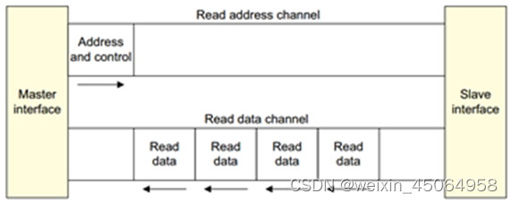
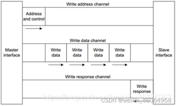
AXI协议将读地址通道,读数据通道,写地址通道,写数据通道,写响应通道分开,各自通道都有自己的握手协议。每个通道互不干扰却又彼此依赖。这是AXI高效的原因之一。
AXI握手协议
AXI4 所采用的是一种 READY,VALID 握手通信机制。即主从模块进行数据通信前,根据操作对各所用到的数据、地址通道进行握手。主要操作包括传输发送者A等到传输接受者B的READY信号后,A将数据与VALID信号同时发送给B。
简单来说主从双方进行数据通信前,有一个握手的过程。传输源产生 VLAID 信号来指明何时数据或控制信息有效。而目地源产生READY信号来指明已经准备好接受数据或控制信息。传输发生在VALID和 READY信号同时为高的时候,如下图所示:
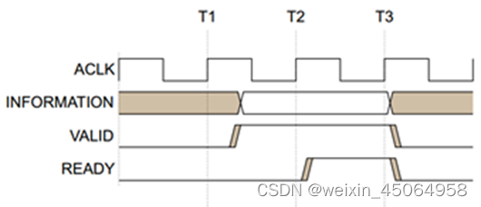
在上图中,ACLK 为时钟信号,在 AXI 协议中,所有的输入信号都在是 ACLK 的上升沿采样,所有的输出信号必须在 ACLK 的上升沿之后才能改变。在 T1 之后,源端将 VALID 拉高,表明 INFORMATION信号线上传输的是有效的地址、数据或者控制信息。目的端在 T2 之后将 READY 拉高,表明它已经准备好接收数据,此时源端必须保持 INFORMATION 数据稳定不变,直到 T3 时刻进行数据传输。
需要注意的是,源端不允许等目的端的 READY 信号拉高之后,才将 VALID 信号置为有效状态。而且,一旦 VALID 拉高,源端必须保持其处于有效状态,直至成功握手(在时钟上升沿检测到 VALID 和 READY同时为有效状态)。
对于AXI总线形式接口的仿真,触发信号应该设置为READY和VLAID同时为1触发,如下图所示。这里设置的是AREADY和AVLAID同时为1触发,表示只有读通道触发,所以读地址通道(AR channel)和读数据通道(R channel)都有显示。而写地址通道(AW channel)显示的是NO Write Addr Cmds,写数据通道(W channel)显示的是NO Write data Cmds。此时写响应通道(B channel)也没有写响应。
反之,如果设置的是WREADY和WVLAID同时为1触发,表示只有写通道触发,所以写数据通道(W channel),写数据通道(W channel)和写响应通道(B channel)都有显示。而读地址通道(AR channel)显示的是NO read Addr Cmds,读数据通道(R channel)显示的是NO read data Cmds。
同一个通道中VALID和READY的先后关系具有三种情况:
• VALID先有效,等待READY有效后完成传输(VALID一旦有效后在传输完成前不可取消)
• READY先有效,等待VALID有效后完成传输(READY可以在VALID有效前撤销)
• VALID和READY同时有效,立刻完成传输
Note:此外,需要注意的是允许READY信号等待VALID信号再有效,即即使从机准备好,也可以不提供READY信号,等到主机发送VALID信号再提供READY信号。对应的VALID信号不允许等待READY信号,即不允许VALID等待READY信号拉高后再拉高,否则容易产生死锁现象。
突发式读写
AXI支持三种突发类型:
- FIXED(AxBURST[1:0]=0b00):固定突发模式,每次突发传输的地址相同;
- INCR(AxBURST[1:0]=0b01):增量突发模式,突发传输地址递增,递增与突发尺寸相关。
- WRAP(AxBURST[1:0]=0b10):回卷突发模式,突发传输地址可溢出性递增,突发长度仅支持2,4,8,16。地址空间被划分为长度【突发尺寸*突发长度】的块,传输地址不会超出起始地址所在的块,一旦递增超出,则回到该块的起始地址。
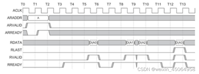
突发式读时序
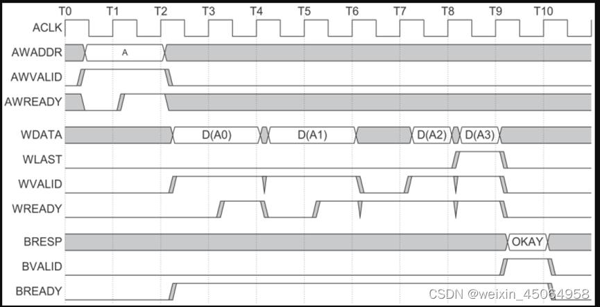
突发式写时序
读/写响应结构
AXI协议提供读/写事务的响应信号:对于读操作,响应信号在读地址通道RRESP[1:0];对于写操作,响应信号在写响应通道BRESP[1:0]。
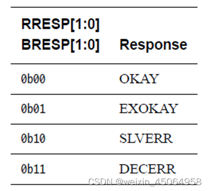
OKAY 常规访问成功
EXOKAY 独占访问成功
SLVERR 从机错误
DECERR 解码错误
读传输实现过程
写传输实现过程
AXI的数据结构
AXI总线是基于突发传输的总线,若主机要开始一次突发传输,需要传输一次地址和相关控制信号,之后从机自动计算地址,但一次突发传输的地址范围不能跨越4KB。
(1)突发长度(AxLEN)
突发长度为每次突发传输的传输次数,范围限制116(AXI4增量模式1256)且不能跨越4kb的地址空间,每次突发传输不允许提前终止(可以通过关闭所有数据字段的方式使一段传输数据无效,但传输行为必须完成)。每次传输的突发长度为AxLEN[3:0] + 1(AXI增量模式AxLEN[7:0] + 1)。
ARLEN[7:0]:读地址通道的突发长度接口;AWLEN[7:0]:写地址通道的突发长度接口。
对于回卷模式突发传输,突发长度仅能是2,4,8或16。
(2)突发尺寸(AxSIZE)
突发尺寸为每次传输的byte数量,与突发传输的地址预测相关性很强。每次的突发尺寸不能超过数据通道的宽度;若突发尺寸小于数据通道宽度,需要指定哪些位数是有效的。
ARSIZE[2:0]:读地址通道突发尺寸;AWSIZE[2:0]:写地址通道突发尺寸。
Main Code
`timescale 1 ns / 1 ps

module my_axi_write_v1_0_M00_AXI #
	(
		// Users to add parameters here

		// User parameters ends
		// Do not modify the parameters beyond this line

		// Base address of targeted slave
		parameter  C_M_TARGET_SLAVE_BASE_ADDR	= 32'h10000000,
		// Burst Length. Supports 1, 2, 4, 8, 16, 32, 64, 128, 256 burst lengths
		parameter integer C_M_AXI_BURST_LEN	= 16,
		// Thread ID Width
		parameter integer C_M_AXI_ID_WIDTH	= 1,
		// Width of Address Bus
		parameter integer C_M_AXI_ADDR_WIDTH	= 32,
		// Width of Data Bus
		parameter integer C_M_AXI_DATA_WIDTH	= 32,
		// Width of User Write Address Bus
		parameter integer C_M_AXI_AWUSER_WIDTH	= 0,
		// Width of User Read Address Bus
		parameter integer C_M_AXI_ARUSER_WIDTH	= 0,
		// Width of User Write Data Bus
		parameter integer C_M_AXI_WUSER_WIDTH	= 0,
		// Width of User Read Data Bus
		parameter integer C_M_AXI_RUSER_WIDTH	= 0,
		// Width of User Response Bus
		parameter integer C_M_AXI_BUSER_WIDTH	= 0
	)
	(
		// Users to add ports here

		input wire   write_pulse,
		input wire   awaddr_en,
		input [31:0] awaddr,
		input [31:0] wdata,


		input wire  	  read_pulse,
		input wire   	  araddr_en,
		input [31:0] 	  araddr,
		output reg[31:0]  rdata,

		// User ports ends
		// Do not modify the ports beyond this line

		output reg   ERROR,

		// Global Clock Signal.
		input wire  M_AXI_ACLK,
		// Global Reset Singal. This Signal is Active Low
		input wire  M_AXI_ARESETN,
		// Master Interface Write Address ID
		output wire [C_M_AXI_ID_WIDTH-1 : 0] M_AXI_AWID,
		// Master Interface Write Address
		output wire [C_M_AXI_ADDR_WIDTH-1 : 0] M_AXI_AWADDR,
		// Burst length. The burst length gives the exact number of transfers in a burst
		output wire [7 : 0] M_AXI_AWLEN,
		// Burst size. This signal indicates the size of each transfer in the burst
		output wire [2 : 0] M_AXI_AWSIZE,
		// Burst type. The burst type and the size information,
    // determine how the address for each transfer within the burst is calculated.
		output wire [1 : 0] M_AXI_AWBURST,
		// Lock type. Provides additional information about the
    // atomic characteristics of the transfer.
		output wire  M_AXI_AWLOCK,
		// Memory type. This signal indicates how transactions
    // are required to progress through a system.
		output wire [3 : 0] M_AXI_AWCACHE,
		// Protection type. This signal indicates the privilege
    // and security level of the transaction, and whether
    // the transaction is a data access or an instruction access.
		output wire [2 : 0] M_AXI_AWPROT,
		// Quality of Service, QoS identifier sent for each write transaction.
		output wire [3 : 0] M_AXI_AWQOS,
		// Optional User-defined signal in the write address channel.
		output wire [C_M_AXI_AWUSER_WIDTH-1 : 0] M_AXI_AWUSER,
		// Write address valid. This signal indicates that
    // the channel is signaling valid write address and control information.
		output wire  M_AXI_AWVALID,
		// Write address ready. This signal indicates that
    // the slave is ready to accept an address and associated control signals
		input wire  M_AXI_AWREADY,
		// Master Interface Write Data.
		output wire [C_M_AXI_DATA_WIDTH-1 : 0] M_AXI_WDATA,
		// Write strobes. This signal indicates which byte
    // lanes hold valid data. There is one write strobe
    // bit for each eight bits of the write data bus.
		output wire [C_M_AXI_DATA_WIDTH/8-1 : 0] M_AXI_WSTRB,
		// Write last. This signal indicates the last transfer in a write burst.
		output wire  M_AXI_WLAST,
		// Optional User-defined signal in the write data channel.
		output wire [C_M_AXI_WUSER_WIDTH-1 : 0] M_AXI_WUSER,
		// Write valid. This signal indicates that valid write
    // data and strobes are available
		output wire  M_AXI_WVALID,
		// Write ready. This signal indicates that the slave
    // can accept the write data.
		input wire  M_AXI_WREADY,
		// Master Interface Write Response.
		input wire [C_M_AXI_ID_WIDTH-1 : 0] M_AXI_BID,
		// Write response. This signal indicates the status of the write transaction.
		input wire [1 : 0] M_AXI_BRESP,
		// Optional User-defined signal in the write response channel
		input wire [C_M_AXI_BUSER_WIDTH-1 : 0] M_AXI_BUSER,
		// Write response valid. This signal indicates that the
    // channel is signaling a valid write response.
		input wire  M_AXI_BVALID,
		// Response ready. This signal indicates that the master
    // can accept a write response.
		output wire  M_AXI_BREADY,
		// Master Interface Read Address.
		output wire [C_M_AXI_ID_WIDTH-1 : 0] M_AXI_ARID,
		// Read address. This signal indicates the initial
    // address of a read burst transaction.
		output wire [C_M_AXI_ADDR_WIDTH-1 : 0] M_AXI_ARADDR,
		// Burst length. The burst length gives the exact number of transfers in a burst
		output wire [7 : 0] M_AXI_ARLEN,
		// Burst size. This signal indicates the size of each transfer in the burst
		output wire [2 : 0] M_AXI_ARSIZE,
		// Burst type. The burst type and the size information,
    // determine how the address for each transfer within the burst is calculated.
		output wire [1 : 0] M_AXI_ARBURST,
		// Lock type. Provides additional information about the
    // atomic characteristics of the transfer.
		output wire  M_AXI_ARLOCK,
		// Memory type. This signal indicates how transactions
    // are required to progress through a system.
		output wire [3 : 0] M_AXI_ARCACHE,
		// Protection type. This signal indicates the privilege
    // and security level of the transaction, and whether
    // the transaction is a data access or an instruction access.
		output wire [2 : 0] M_AXI_ARPROT,
		// Quality of Service, QoS identifier sent for each read transaction
		output wire [3 : 0] M_AXI_ARQOS,
		// Optional User-defined signal in the read address channel.
		output wire [C_M_AXI_ARUSER_WIDTH-1 : 0] M_AXI_ARUSER,
		// Write address valid. This signal indicates that
    // the channel is signaling valid read address and control information
		output wire  M_AXI_ARVALID,
		// Read address ready. This signal indicates that
    // the slave is ready to accept an address and associated control signals
		input wire  M_AXI_ARREADY,
		// Read ID tag. This signal is the identification tag
    // for the read data group of signals generated by the slave.
		input wire [C_M_AXI_ID_WIDTH-1 : 0] M_AXI_RID,
		// Master Read Data
		input wire [C_M_AXI_DATA_WIDTH-1 : 0] M_AXI_RDATA,
		// Read response. This signal indicates the status of the read transfer
		input wire [1 : 0] M_AXI_RRESP,
		// Read last. This signal indicates the last transfer in a read burst
		input wire  M_AXI_RLAST,
		// Optional User-defined signal in the read address channel.
		input wire [C_M_AXI_RUSER_WIDTH-1 : 0] M_AXI_RUSER,
		// Read valid. This signal indicates that the channel
    // is signaling the required read data.
		input wire  M_AXI_RVALID,
		// Read ready. This signal indicates that the master can
    // accept the read data and response information.
		output wire  M_AXI_RREADY
	);


	// function called clogb2 that returns an integer which has the
	//value of the ceiling of the log base 2

	  // function called clogb2 that returns an integer which has the
	  // value of the ceiling of the log base 2.
	 function integer clogb2 (input integer bit_depth);
	  begin
	    for(clogb2=0; bit_depth>0; clogb2=clogb2+1)
	      bit_depth = bit_depth >> 1;
	    end
	  endfunction

	// C_TRANSACTIONS_NUM is the width of the index counter for
	// number of write or read transaction.
	 localparam integer C_TRANSACTIONS_NUM = clogb2(C_M_AXI_BURST_LEN-1);

	// Burst length for transactions, in C_M_AXI_DATA_WIDTHs.
	// Non-2^n lengths will eventually cause bursts across 4K address boundaries.
	 localparam integer C_MASTER_LENGTH	= 12;
	// total number of burst transfers is master length divided by burst length and burst size
	 localparam integer C_NO_BURSTS_REQ = C_MASTER_LENGTH-clogb2((C_M_AXI_BURST_LEN*C_M_AXI_DATA_WIDTH/8)-1);
	// Example State machine to initialize counter, initialize write transactions,
	// initialize read transactions and comparison of read data with the
	// written data words.


	// AXI4LITE signals
	//AXI4 internal temp signals
	reg [C_M_AXI_ADDR_WIDTH-1 : 0] 	axi_awaddr;
	reg  	axi_awvalid;
	reg [C_M_AXI_DATA_WIDTH-1 : 0] 	axi_wdata;
	reg  	axi_wlast;
	reg  	axi_wvalid;
	reg  	axi_bready;
	reg [C_M_AXI_ADDR_WIDTH-1 : 0] 	axi_araddr;
	reg  	axi_arvalid;
	reg  	axi_rready;
	//write beat count in a burst
	reg [C_TRANSACTIONS_NUM : 0] 	write_index;
	//read beat count in a burst
	reg [C_TRANSACTIONS_NUM : 0] 	read_index;
	//size of C_M_AXI_BURST_LEN length burst in bytes
	wire [C_TRANSACTIONS_NUM+2 : 0] 	burst_size_bytes;
	//The burst counters are used to track the number of burst transfers of C_M_AXI_BURST_LEN burst length needed to transfer 2^C_MASTER_LENGTH bytes of data.
	reg [C_NO_BURSTS_REQ : 0] 	write_burst_counter;
	reg [C_NO_BURSTS_REQ : 0] 	read_burst_counter;
	reg  	start_single_burst_write;
	reg  	start_single_burst_read;
	reg  	writes_done;
	reg  	reads_done;
	reg  	error_reg;
	reg  	compare_done;
	reg  	read_mismatch;
	reg  	burst_write_active;
	reg  	burst_read_active;
	reg [C_M_AXI_DATA_WIDTH-1 : 0] 	expected_rdata;
	//Interface response error flags
	wire  	write_resp_error;
	wire  	read_resp_error;
	wire  	wnext;
	wire  	rnext;
	reg  	init_txn_ff;
	reg  	init_txn_ff2;
	reg  	init_txn_edge;
	wire  	init_txn_pulse;


	// I/O Connections assignments

	//I/O Connections. Write Address (AW)
	assign M_AXI_AWID	= 'b0;
	//The AXI address is a concatenation of the target base address + active offset range
	assign M_AXI_AWADDR	= C_M_TARGET_SLAVE_BASE_ADDR + axi_awaddr;
	//Burst LENgth is number of transaction beats, minus 1
	assign M_AXI_AWLEN	= C_M_AXI_BURST_LEN - 1;
	//Size should be C_M_AXI_DATA_WIDTH, in 2^SIZE bytes, otherwise narrow bursts are used
	assign M_AXI_AWSIZE	= clogb2((C_M_AXI_DATA_WIDTH/8)-1);
	//INCR burst type is usually used, except for keyhole bursts
	assign M_AXI_AWBURST	= 2'b01;
	assign M_AXI_AWLOCK	= 1'b0;
	//Update value to 4'b0011 if coherent accesses to be used via the Zynq ACP port. Not Allocated, Modifiable, not Bufferable. Not Bufferable since this example is meant to test memory, not intermediate cache.
	assign M_AXI_AWCACHE	= 4'b0010;
	assign M_AXI_AWPROT	= 3'h0;
	assign M_AXI_AWQOS	= 4'h0;
	assign M_AXI_AWUSER	= 'b1;
	assign M_AXI_AWVALID	= axi_awvalid;
	//Write Data(W)
	assign M_AXI_WDATA	= axi_wdata;
	//All bursts are complete and aligned in this example
	assign M_AXI_WSTRB	= {(C_M_AXI_DATA_WIDTH/8){1'b1}};
	assign M_AXI_WLAST	= axi_wlast;
	assign M_AXI_WUSER	= 'b0;
	assign M_AXI_WVALID	= axi_wvalid;
	//Write Response (B)
	assign M_AXI_BREADY	= axi_bready;
	//Read Address (AR)
	assign M_AXI_ARID	= 'b0;
	assign M_AXI_ARADDR	= C_M_TARGET_SLAVE_BASE_ADDR + axi_araddr;
	//Burst LENgth is number of transaction beats, minus 1
	assign M_AXI_ARLEN	= C_M_AXI_BURST_LEN - 1;
	//Size should be C_M_AXI_DATA_WIDTH, in 2^n bytes, otherwise narrow bursts are used
	assign M_AXI_ARSIZE	= clogb2((C_M_AXI_DATA_WIDTH/8)-1);
	//INCR burst type is usually used, except for keyhole bursts
	assign M_AXI_ARBURST	= 2'b01;
	assign M_AXI_ARLOCK	= 1'b0;
	//Update value to 4'b0011 if coherent accesses to be used via the Zynq ACP port. Not Allocated, Modifiable, not Bufferable. Not Bufferable since this example is meant to test memory, not intermediate cache.
	assign M_AXI_ARCACHE	= 4'b0010;
	assign M_AXI_ARPROT	= 3'h0;
	assign M_AXI_ARQOS	= 4'h0;
	assign M_AXI_ARUSER	= 'b1;
	assign M_AXI_ARVALID	= axi_arvalid;
	//Read and Read Response (R)
	assign M_AXI_RREADY	= axi_rready;
	//Example design I/O
	assign TXN_DONE	= compare_done;
	//Burst size in bytes
	assign burst_size_bytes	= C_M_AXI_BURST_LEN * C_M_AXI_DATA_WIDTH/8;


	/*assign awaddr_en = 'b0;
	assign awaddr    = 'd0;
	assign wdata	 = 'd0;

	assign araddr_en = 1'b0;
	assign araddr	 = 'd0;*/


	//--------------------
	//Write or read Pulse synchronous
	//--------------------
	reg write_ff0,write_ff1;
	reg read_ff0,read_ff1;
	wire write_start,read_start;

	assign write_start	= (!write_ff0) && write_ff1; // negedeg 写使能
	assign read_start	= (!read_ff0) && read_ff1;
	//Generate a pulse to initiate AXI transaction. 信号同步时钟
	always @(posedge M_AXI_ACLK)
	  begin
	    // Initiates AXI transaction delay
	    if (M_AXI_ARESETN == 0)
	      begin
			{write_ff0,write_ff1,read_ff0,read_ff1} <= 4'b0000;
	      end
	    else
	      begin
	        {write_ff1,write_ff0} <= {write_ff0,write_pulse};
			{read_ff1,read_ff0}   <= {read_ff0,read_pulse};
	      end
	  end

	//--------------------
	//Write Address Channel
	//--------------------

	// The purpose of the write address channel is to request the address and
	// command information for the entire transaction.  It is a single beat
	// of information.

	// The AXI4 Write address channel in this example will continue to initiate
	// write commands as fast as it is allowed by the slave/interconnect.
	// The address will be incremented on each accepted address transaction,
	// by burst_size_byte to point to the next address.

	always @(posedge M_AXI_ACLK)
	  begin
	    if (M_AXI_ARESETN == 0 || write_start == 1'b1 )
	      begin
	        axi_awvalid <= 1'b0;
	      end
	    // If previously not valid , start next transaction
	    else if (~axi_awvalid && start_single_burst_write)
	      begin
	        axi_awvalid <= 1'b1;
	      end
	    /* Once asserted, VALIDs cannot be deasserted, so axi_awvalid
	    must wait until transaction is accepted */
	    else if (M_AXI_AWREADY && axi_awvalid)
	      begin
	        axi_awvalid <= 1'b0;
	      end
	    else
	      axi_awvalid <= axi_awvalid;
	    end


	// Next address after AWREADY indicates previous address acceptance
	always @(posedge M_AXI_ACLK)
	  begin
	    if (M_AXI_ARESETN == 0)
	      begin
	        axi_awaddr <= 'b0;
	      end
		else if(awaddr_en)
			axi_awaddr <= awaddr;
	    else if (M_AXI_AWREADY && axi_awvalid)
	      begin
	        axi_awaddr <= axi_awaddr + burst_size_bytes;
	      end
	    else
	      axi_awaddr <= axi_awaddr;
	    end

	//--------------------
	//Write Data Channel
	//--------------------
	//Forward movement occurs when the write channel is valid and ready

	  assign wnext = M_AXI_WREADY & axi_wvalid;

	// WVALID logic, similar to the axi_awvalid always block above
	always @(posedge M_AXI_ACLK)
	  begin
	    if (M_AXI_ARESETN == 0 || write_start == 1'b1 )
	      begin
	        axi_wvalid <= 1'b0;
	      end
	    // If previously not valid, start next transaction
	    else if (~axi_wvalid && start_single_burst_write)
	      begin
	        axi_wvalid <= 1'b1;
	      end
	    /* If WREADY and too many writes, throttle WVALID
	    Once asserted, VALIDs cannot be deasserted, so WVALID
	    must wait until burst is complete with WLAST */
	    else if (wnext && axi_wlast)
	      axi_wvalid <= 1'b0;
	    else
	      axi_wvalid <= axi_wvalid;
	  end


	//WLAST generation on the MSB of a counter underflow
	// WVALID logic, similar to the axi_awvalid always block above
	 always @(posedge M_AXI_ACLK)
	  begin
	    if (M_AXI_ARESETN == 0 || write_start == 1'b1 )
	      begin
	        axi_wlast <= 1'b0;
	      end
	    // axi_wlast is asserted when the write index
	    // count reaches the penultimate count to synchronize
	    // with the last write data when write_index is b1111
	    // else if (&(write_index[C_TRANSACTIONS_NUM-1:1])&& ~write_index[0] && wnext)
	    else if (((write_index == C_M_AXI_BURST_LEN-2 && C_M_AXI_BURST_LEN >= 2) && wnext) || (C_M_AXI_BURST_LEN == 1 ))
	      begin
	        axi_wlast <= 1'b1;
	      end
	    // Deassrt axi_wlast when the last write data has been
	    // accepted by the slave with a valid response
	    else if (wnext)
	      axi_wlast <= 1'b0;
	    else if (axi_wlast && C_M_AXI_BURST_LEN == 1)
	      axi_wlast <= 1'b0;
	    else
	      axi_wlast <= axi_wlast;
	  end

	always @(posedge M_AXI_ACLK)
	  begin
	    if (M_AXI_ARESETN == 0 || write_start == 1'b1 || start_single_burst_write == 1'b1)
	      begin
	        write_index <= 0;
	      end
	    else if (wnext && (write_index != C_M_AXI_BURST_LEN-1))
	      begin
	        write_index <= write_index + 1;
	      end
	    else
	      write_index <= write_index;
	  end


	 /* Write Data Generator
	 Data pattern is only a simple incrementing count from 0 for each burst*/

	always @(posedge M_AXI_ACLK)
	  begin
	    if (M_AXI_ARESETN == 0 || write_start == 1'b1)
	      axi_wdata <= 'd0;
	    //else if (wnext && axi_wlast)
	    //  axi_wdata <= 'b0;
	    else if (wnext)
	      axi_wdata <= axi_wdata + 1;
	    else
	      axi_wdata <= axi_wdata;
	    end

	//----------------------------
	//Write Response (B) Channel
	//----------------------------
	always @(posedge M_AXI_ACLK)
	  begin
	    if (M_AXI_ARESETN == 0 || write_start == 1'b1 )
	      begin
	        axi_bready <= 1'b0;
	      end
	    // accept/acknowledge bresp with axi_bready by the master
	    // when M_AXI_BVALID is asserted by slave
	    else if (M_AXI_BVALID && ~axi_bready)
	      begin
	        axi_bready <= 1'b1;
	      end
	    // deassert after one clock cycle
	    else if (axi_bready)
	      begin
	        axi_bready <= 1'b0;
	      end
	    // retain the previous value
	    else
	      axi_bready <= axi_bready;
	  end


	//Flag any write response errors
	  assign write_resp_error = axi_bready & M_AXI_BVALID & M_AXI_BRESP[1];


	always @ ( posedge M_AXI_ACLK)
	  begin
	    if (M_AXI_ARESETN == 1'b0 )
	      begin
	        // reset condition
	        // All the signals are assigned default values under reset condition
	        start_single_burst_write <= 1'b0;
	        //start_single_burst_read  <= 1'b0;
	      end
		else if(write_start&&~axi_awvalid && ~start_single_burst_write && ~burst_write_active)
	       begin
			start_single_burst_write <= 1'b1;
		   end
		else
		   begin
			start_single_burst_write <= 1'b0; //Negate to generate a pulse
		   end
		 end


	  // write state ==> burst_write_active
	  // burst_write_active signal is asserted when there is a burst write transaction
	  // is initiated by the assertion of start_single_burst_write. burst_write_active
	  // signal remains asserted until the burst write is accepted by the slave
	  always @(posedge M_AXI_ACLK)
	  begin
	    if (M_AXI_ARESETN == 0 || write_start == 1'b1)
	      burst_write_active <= 1'b0;
	    //The burst_write_active is asserted when a write burst transaction is initiated
	    else if (start_single_burst_write)
	      burst_write_active <= 1'b1;
	    else if (M_AXI_BVALID && axi_bready)
	      burst_write_active <= 1'b0;
	  end


	//----------------------------
	//Read Address Channel
	//----------------------------

  always @(posedge M_AXI_ACLK)
	  begin

	    if (M_AXI_ARESETN == 0 || read_start == 1'b1 )
	      begin
	        axi_arvalid <= 1'b0;
	      end
	    // If previously not valid , start next transaction
	    else if (~axi_arvalid && start_single_burst_read)
	      begin
	        axi_arvalid <= 1'b1;
	      end
	    else if (M_AXI_ARREADY && axi_arvalid)
	      begin
	        axi_arvalid <= 1'b0;
	      end
	    else
	      axi_arvalid <= axi_arvalid;
	  end

	 // Next address after ARREADY indicates previous address acceptance
	 always @(posedge M_AXI_ACLK)
	  begin
	    if (M_AXI_ARESETN == 0 )
	      begin
	        axi_araddr <= 'b0;
	      end
		else if(araddr_en)
		  begin
	        axi_araddr <= araddr;
	      end
	    else if (M_AXI_ARREADY && axi_arvalid)
	      begin
	        axi_araddr <= axi_araddr + burst_size_bytes;
	      end
	    else
	      axi_araddr <= axi_araddr;
	  end

	//--------------------------------
	//Read Data (and Response) Channel
	//--------------------------------
	// Forward movement occurs when the channel is valid and ready
	  assign rnext = M_AXI_RVALID && axi_rready;

	// Burst length counter. Uses extra counter register bit to indicate
	// terminal count to reduce decode logic
	  always @(posedge M_AXI_ACLK)
	  begin
	    if (M_AXI_ARESETN == 0 || start_single_burst_read)
	      begin
	        read_index <= 0;
	      end
	    else if (rnext && (read_index != C_M_AXI_BURST_LEN-1))
	      begin
	        read_index <= read_index + 1;
	      end
	    else
	      read_index <= read_index;
	  end

	/*
	 The Read Data channel returns the results of the read request
	 In this example the data checker is always able to accept
	 more data, so no need to throttle the RREADY signal
	 */
	always @(posedge M_AXI_ACLK)
	  begin
	    if (M_AXI_ARESETN == 0 || read_start == 1'b1 )
	      begin
	        axi_rready <= 1'b0;
	      end
	    // accept/acknowledge rdata/rresp with axi_rready by the master
	    // when M_AXI_RVALID is asserted by slave
	    else if (M_AXI_RVALID)
	      begin
	         if (M_AXI_RLAST && axi_rready)
	          begin
	            axi_rready <= 1'b0;
	          end
	         else
	           begin
	             axi_rready <= 1'b1;
	           end
	      end
	    // retain the previous value
	  end


assign read_resp_error = axi_rready & M_AXI_RVALID & M_AXI_RRESP[1];
	always @(posedge M_AXI_ACLK)
	  begin
	    if (M_AXI_ARESETN == 0 || read_start || write_start)
	      begin
	        error_reg <= 1'b0;
	      end
	    else if (write_resp_error || read_resp_error)
	      begin
	        error_reg <= 1'b1;
	      end
	    else
	      error_reg <= error_reg;
	  end


	always@(posedge M_AXI_ACLK)
		begin
			 if (read_start && ~axi_arvalid && ~burst_read_active && ~start_single_burst_read)
			  begin
				start_single_burst_read <= 1'b1;
			  end
		   else
			 begin
			   start_single_burst_read <= 1'b0; //Negate to generate a pulse
			 end
		end

	always@(posedge M_AXI_ACLK)
		if(!M_AXI_ARESETN || read_start)
			burst_read_active <= 1'b0;
		else if(start_single_burst_read)
			burst_read_active <= 1'b1;
		else if(M_AXI_RLAST && axi_rready&&M_AXI_RVALID)
			burst_read_active <= 1'b0;
		else
			burst_read_active <= burst_read_active;

endmodule
SDK code
#include"stdio.h"
#include "xil_io.h"
#include"xil_cache.h"
#include"xil_printf.h"
#include "xparameters.h"
#include "xgpiops.h"
#include "sleep.h"
#include "xstatus.h"
#include "xplatform_info.h"

#define GPIO_DEVICE_ID  XPAR_XGPIOPS_0_DEVICE_ID
#define Output_pin0   55
#define Input_pin0    54
#define GPIO_BANK	XGPIOPS_BANK2


#define BaseAddress 0x10000000

void GpioOutput(u32 Output_Pin,u32 data);//instance of Gpio input with data;
int GpioInput(u32 Input_Pin,u32 DataRead);// instance of Gpio input with data;

XGpioPs Gpio; /* The Instance of the GPIO Driver */
int main()
{

	Xil_DCacheDisable();  //关闭缓存

	XGpioPs_Config *ConfigPtr;
	ConfigPtr = XGpioPs_LookupConfig(GPIO_DEVICE_ID);
	XGpioPs_CfgInitialize(&Gpio, ConfigPtr,ConfigPtr->BaseAddr);
	printf("AXI test start!\n");

	u32 data = 1;
	u32 datai =0;
	int bia  = 0;
	//char c;
	//int data;
	while(1)
	{
		if(GpioInput(Input_pin0,datai))
		{
			for(int i = 0;i < 64;i = i+4)
			{
				data = Xil_In32(BaseAddress + bia+ i);//取地址的数据
				printf("%d => %d\n",i,data);
			}
			bia = bia + 64;
		sleep(1);
		}
	}
}

void GpioOutput(u32 Output_Pin,u32 data)
{
	 //Set the direction for the pin to be output or input (1 or 0);
	XGpioPs_SetDirectionPin(&Gpio, Output_Pin, 1);

	 // Enable the Output enable for the LED Pin.
	XGpioPs_SetOutputEnablePin(&Gpio, Output_Pin, 1);

	/* Set the GPIO output to be data. */
	XGpioPs_WritePin(&Gpio, Output_Pin, data);
}

int  GpioInput(u32 Input_Pin,u32 DataRead)
 {
 	/* Set the direction for the specified pin to be input. */
 	XGpioPs_SetDirectionPin(&Gpio, Input_Pin, 0x0);

 	/* Read the state of the data so that it can be  verified. */
 	DataRead = XGpioPs_ReadPin(&Gpio, Input_Pin);

 	return DataRead;
 }


 6316
6316

 被折叠的 条评论
为什么被折叠?
被折叠的 条评论
为什么被折叠?
 到【灌水乐园】发言


