


目录
5\ DFF WITH ASYNCHRONOUS RESET
1\ D FLIP-FLOP
A D flip-flop is a circuit that stores a bit and is updated periodically, at the (usually) positive edge of a clock signal.
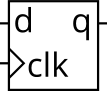
D flip-flops are created by the logic synthesizer when a clocked always block is used (See alwaysblock2). A D flip-flop is the simplest form of "blob of combinational logic followed by a flip-flop" where the combinational logic portion is just a wire.
Create a single D flip-flop.
HINT:
用always块写一个D触发器。
CORRECT:
module top_module (
input clk, // Clocks are used in sequential circuits
input d,
output reg q );//
always@(posedge clk)
q<=d;
endmodule
2\ D FLIP-FLOPS
Create 8 D flip-flops. All DFFs should be triggered by the positive edge of clk.
CORRECT:
module top_module (
input clk,
input [7:0] d,
output [7:0] q
);
always@(posedge clk)
q<=d;
endmodule
3\ DFF WITH RESET
Create 8 D flip-flops with active high synchronous reset. All DFFs should be triggered by the positive edge of clk.
ERRO:
module top_module (
input clk,
input reset, // Synchronous reset
input [7:0] d,
output [7:0] q
);
always @ (posedge clk or negedge reset) //缺begin end
if (reset)
q<=0;
else
q<=d;
endmodule
CORRECT:
module top_module (
input clk,
input reset, // Synchronous reset
input [7:0] d,
output [7:0] q
);
always @ (posedge clk)
begin
if(reset==1)
q<=0;
else
q<=d;
end
endmodule
4\ DFF WITH RESET VALUE
Create 8 D flip-flops with active high synchronous reset. The flip-flops must be reset to 0x34 rather than zero. All DFFs should be triggered by the negative edge of clk.
HINT:
Resetting a register to '1' is sometimes called "preset"
在Verilog中,常数的写法有以下几种非法写法:
1、‘与基数(h,b,o,d)之间不允许有空格;
2、数值不能为负数,有负号的话应放在最左边;
3、位宽不能为表达式。
CORRECT:
module top_module (
input clk,
input reset, // Synchronous reset
input [7:0] d,
output [7:0] q
);
always @ (negedge clk)
begin
if(reset)
q<=8'h0x34;
else
q<=d;
end
endmodule
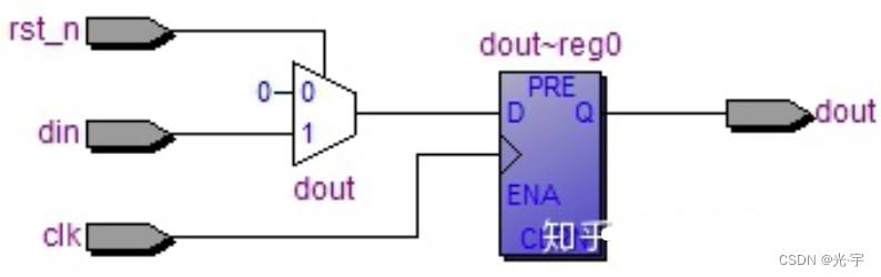
5\ DFF WITH ASYNCHRONOUS RESET
Create 8 D flip-flops with active high asynchronous reset. All DFFs should be triggered by the positive edge of clk.
HINT:
The only difference in code between synchronous and asynchronous reset flip-flops is in the sensitivity list.
同步复位:
同步复位:是指当复位信号发生变化时,并不立即生效,只有当有效时钟沿采样到已变化的复位信号后,才对所有寄存器复位。
同步复位电路如下图所示:
always @(posedge clk) begin
if(!rst_n)
dout <= 0;
else
dout <= din;
end
异步复位:
异步复位: 无论时钟沿是否到来,只要复位信号有效,就对系统进行复位
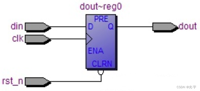
always @(posedge clk or negedge rst_n) begin
if(!rst_n)
dout <= 0;
else
dout <= din;
end
CORRECT:
module top_module (
input clk,
input areset, // active high asynchronous reset
input [7:0] d,
output [7:0] q
);
always @(posedge clk,posedge areset)
begin
if(areset)
q<=0;
else
q<=d;
end
endmodule
6\ DFF WITH BYTE ENABLE
Create 16 D flip-flops. It's sometimes useful to only modify parts of a group of flip-flops. The byte-enable inputs control whether each byte of the 16 registers should be written to on that cycle. byteena[1] controls the upper byte d[15:8], while byteena[0] controls the lower byte d[7:0].(创建16位D触发器。有时只修改一组触发器的部分是有用的。允许字节的输入控制16个寄存器中的每个字节是否应该在那个循环中写入。Byteena[1]控制上字节d[15:8],而Byteena[0]控制下字节d[7:0]。)
resetn is a synchronous, active-low reset.(复位是同步的,主动低复位。)
All DFFs should be triggered by the positive edge of clk.
CORRECT:
module top_module (
input clk,
input resetn,
input [1:0] byteena,
input [15:0] d,
output [15:0] q
);
always @(posedge clk)
begin
if (!resetn)
q<=0;
else
begin /else里面别忘了加begin end!!!!!!!!!!!
if(byteena[0])
q[7:0]<=d[7:0];
else
q[7:0]<=q[7:0];
if(byteena[1])
q[15:8]<=d[15:8];
else
q[15:8]<=q[15:8];
end
end
endmodule
7\ D LATCH
Implement the following circuit:
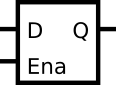
Note that this is a latch, so a Quartus warning about having inferred a latch is expected.
HINT:
- Latches are level-sensitive (not edge-sensitive) circuits, so in an always block, they use level-sensitive sensitivity lists.
- However, they are still sequential elements, so should use non-blocking assignments.
- A D-latch acts like a wire (or non-inverting buffer) when enabled, and preserves the current value when disabled.
(锁存是水平敏感(不是边缘敏感)电路,因此在always块中,它们使用水平敏感的灵敏度列表。
但是,它们仍然是顺序元素,因此应该使用非阻塞赋值。D-latch在启用时就像导线(或非反转缓冲器),在禁用时保持当前值。)
这就是D锁存器。
锁存器对脉冲的电平敏感,也就是电平触发,在有效的电平下,锁存器处于使能状态,输出随着输入发生变化,此时它不锁存信号,就像一个缓冲器一样;在锁存器没有使能时,则数据被锁住,输入信号不起作用,此时输出一直为锁存的状态信息(锁存最后一拍数据)。我们常见的锁存器有SR锁存器、D锁存器、JK锁存器等
CORRECT:
module top_module (
input d,
input ena,
output q);
always@(*)
begin
if(ena)
q<=d;
end
endmodule
ERRO:
module top_module (
input d,
input ena,
output q);
always@(*)
begin
if(ena)
q<=d;
else
q<=0;
end
endmodule
8\ DFF
Implement the following circuit:
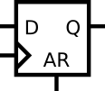
CORRECT:
module top_module (
input clk,
input d,
input ar, // asynchronous reset 异步
output q);
always@(posedge clk or posedge ar)
begin
if(ar)
q<=0;
else
q<=d;
end
endmodule
9\ DFF
Implement the following circuit:
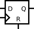
module top_module (
input clk,
input d,
input r, // synchronous reset 同步
output q);
always@(posedge clk)
begin
if(r)
q<=0;
else
q<=d;
end
endmodule


 1151
1151


 被折叠的 条评论
为什么被折叠?
被折叠的 条评论
为什么被折叠?
 到【灌水乐园】发言


