


一.要求:利用Block Design设计一个三位 4 选 1 多路选择器电路
二.实验原理:
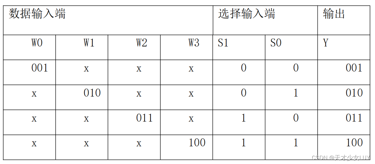
真值表:
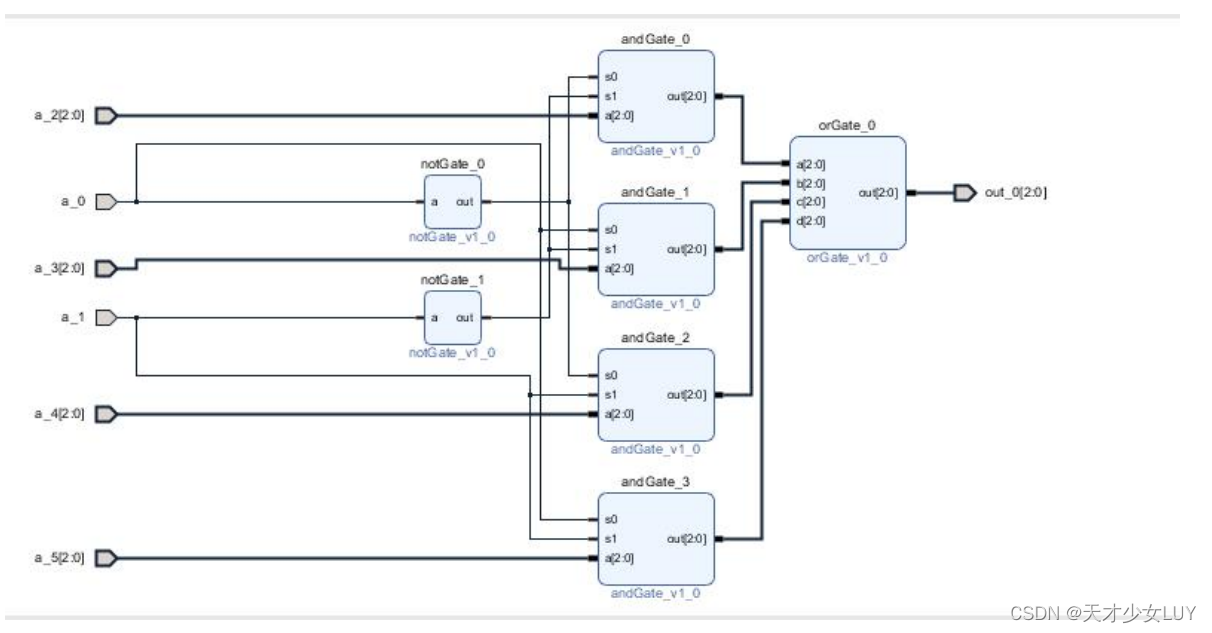
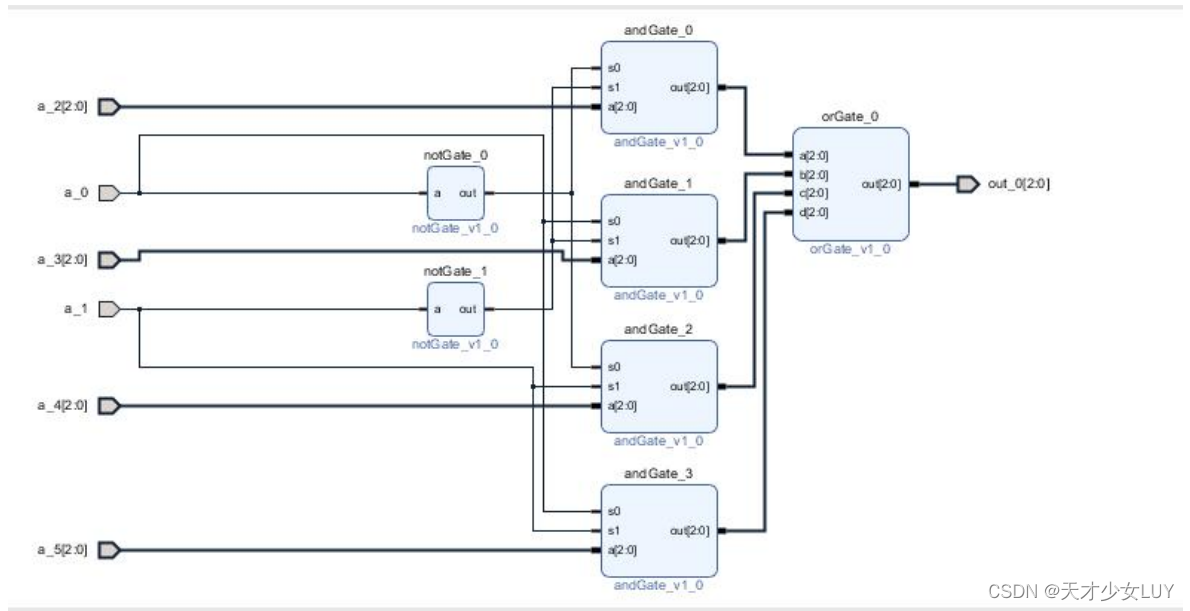
Block Design原理图
三.设计过程
Block Design 将自己编写的与门,非门和或门封装成三个独立的 IP 核,在另一个 Project 中导入后,进行连线设计,然后写出 design 代码。
1)编写与门,或门,非门
1.与门:输入的每一位都和 S0,S1 相与
module andGate #(parameter SIZE = 3)
(input s0, input s1, input[(SIZE-1):0] a, output[(SIZE-1):0] out);
 genvar i;
 generate for(i=0;i<SIZE;i=i+1)
 begin: gfor
 assign out[i] = a[i]&s0&s1;
 end
 endgenerate
 endmodule
2.或门:输出的每 i 位等于每一个输入数据第 i 位相或
module orGate #(parameter SIZE = 3)
(input [(SIZE-1):0] a, input[(SIZE-1):0] b, input[(SIZE-1):0] c, input [(SIZE-1):0] d, output [(SIZE-1):0] out); genvar i;
generate for(i=0; i<SIZE; i=i+1)
begin: gfor
assign out[i] = a[i]|b[i]|c[i]|d[i];
end
endgenerate
endmodule
3.非门:对输入进行取反操作
module notGate#(parameter SIZE = 3)
(input a, output out);
assign out = ~a;
endmodule
2) 进行 Block Design, 电路连线及代码编写
设计思路:根据 0 和任何数相与都得 0,而只有当三个数全为 1 相与时才 能为 1。要想输入 00 时输出为 001,则他需要将选择信号取反后再和 001 相与才能得到 001。同理要输入 01 得到 010,则选择信号低位取 反,高位不变后再与 010 相与则可输出 010。对 10 和 011,11 和 100 同 理,设计好四个与门后,将四个与门的输出连到或门,进行每一位相 或,则可以得到正确输出。
1.电路连线
2.代码编写
a_0 和 a_1 为两位选择信号,a_2,a_3,a_4,a_5 均为三位输入的数据, out_0 为三位选择的输出数据。 design_1 为上图所示的 block design 文件,用 a_0 到 a_5 实例化一个名 为 h1 的 design_1 的 block design。
module mux4to1_bd (a_0,a_1,a_2,a_3,a_4,a_5,out_0);
input a_0;
input a_1;
input[2:0] a_2;
input[2:0] a_3;
input[2:0] a_4;
input[2:0] a_5;
output [2:0] out_0;
design_1 hl(.a_0(a_0),.a_1(a_1),.a_2(a_2),.a_3(a_3),.a_4(a_4),.a_5(a_5),.out_0 (out_0));
endmodule
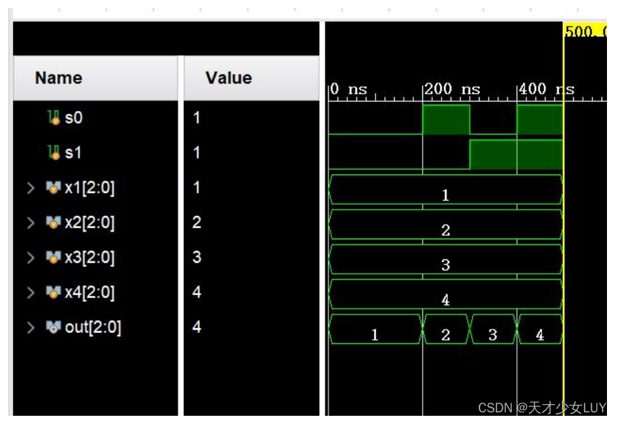
四.仿真
1.仿真文件
`timescale 1ns / 1ps module mux4to1_bd_try();
reg s0,s1;
reg [2:0] x1;
reg [2:0] x2;
reg [2:0] x3;
reg [2:0] x4;
wire [2:0] out;
mux4to1_bd try(s0,s1,x1,x2,x3,x4,out);
initial
	begin
		s0 = 0; s1 = 0;
		x1 = 3'b001; x2 = 3'b010;
		x3 = 3'b011; x4 = 3'b100;
		#100
		s0 = 0; s1 = 0;
		#100
		s0 = 1; s1 = 0;
		#100
		s0 = 0; s1 = 1;
		#100
		s0 = 1; s1 = 1;
		#100
		$stop;
		end
	endmodule
2.仿真结果
记得点赞收藏喏


 6972
6972

 被折叠的 条评论
为什么被折叠?
被折叠的 条评论
为什么被折叠?
 到【灌水乐园】发言


