


项目场景:
You're familiar with flip-flops that are triggered on the positive edge of the clock, or negative edge of the clock. A dual-edge triggered flip-flop is triggered on both edges of the clock. However, FPGAs don't have dual-edge triggered flip-flops, and always @(posedge clk or negedge clk) is not accepted as a legal sensitivity list.
Build a circuit that functionally behaves like a dual-edge triggered flip-flop:
(Note: It's not necessarily perfectly equivalent: The output of flip-flops have no glitches, but a larger combinational circuit that emulates this behaviour might. But we'll ignore this detail here.)
问题描述
你应该很熟悉在时钟的正边或负边触发的触发器。双边触发触发器在时钟的两端被触发。然而,fpga没有双边触发触发器,并且总是@(posedge clk or negedge clk)不被接受合法的敏感列表。
构建一个功能上类似于双边触发器的电路。
(注:这并不一定是完全等价的:触发器的输出没有故障,但模拟这种行为的更大的组合电路可能会有。但这里我们将忽略这个细节。)
原因分析:
这个问题看起来并不复杂,但是当我们使用@(posedge clk or negedge clk)会发现这条语句是不被接受的。单独绘制上升沿触发和下降沿触发的波形图,二者和输出q进行对比我们可以发现三者之间的关系。当clk=1 时,q取的是上升沿触发的d值,当clk= 0 时,q取的是下降沿触发的d值。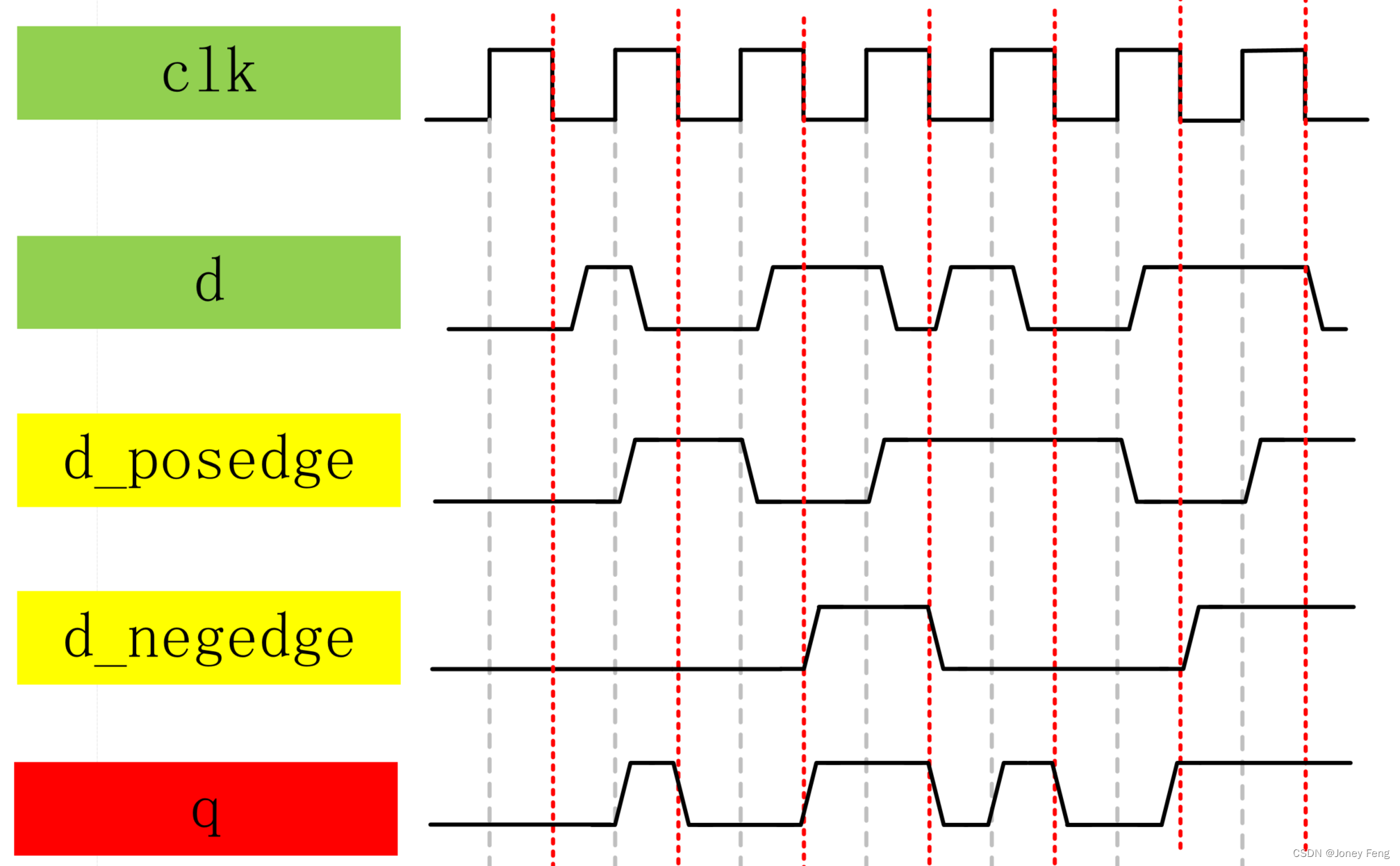
解决方案:
module top_module (
    input clk,
    input d,
    output q
);
 	reg			d_posedge;
    reg			d_negedge;
    always@(posedge	clk )
    	d_posedge <= d;

    always@(negedge	clk )
    	d_negedge <= d;

    assign	q = clk ? d_posedge : d_negedge;

endmodule
运行结构如下:


 1016
1016


 被折叠的 条评论
为什么被折叠?
被折叠的 条评论
为什么被折叠?
 到【灌水乐园】发言


