GT Transceiver中的重要时钟及其关系(5)QPLL的工作原理介绍

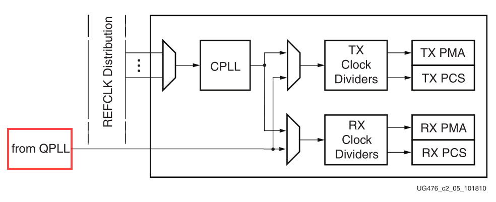
每个QUAD都包含一个QPLL,QPLL可以被同一个Quad内的transceiver共享,但是不能被其他Quad内的transceiver共享。

当以高于CPLL操作范围的线速率操作通道时,需要使用 QPLL。

GTXE2_COMMON 原语封装了 GTX QPLL,并且必须在使用 GTX QPLL时实例化。

QPLL输出为同一Quad内的每个transceiver的TX和RX时钟分频器块提供信号,该块控制PMA和PCS块使用的串行和并行时钟的生成。

QPLL

下图为QPLL架构的概念视图:

QPLL架构概念视图

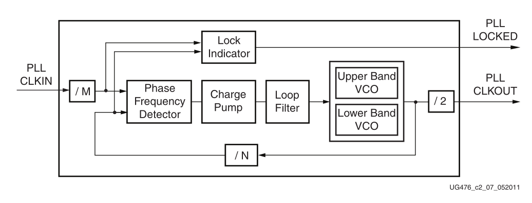
关于,其架构概念框图的描述,和CPLL几乎一致:

输入的时钟在进入相位频率检测器之前可以被除以一个系数M。反馈分频器N决定了VCO的乘法比率。QPLL的输出频率是VCO频率的一半。锁定指示块比较参考时钟和VCO反馈时钟的频率,以确定是否已经实现了频率锁定。

QPLL VCO在两个不同的频段内工作。下表描述了这些Band的标称工作范围。

QPLL标称工作频段
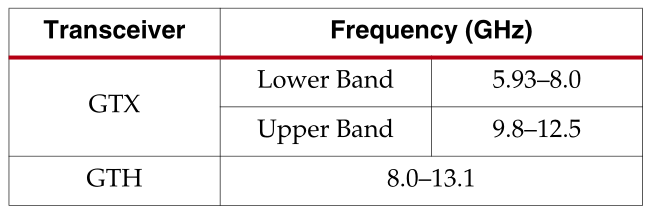
当选择低频段VCO时,高频段VCO会自动断电,反之亦然。7系列FPGA Transceiver向导根据应用要求选择适当的频段和QPLL设置。

下面两个公式分别决定了QPLL的输出频率GHz以及transceiver线速率:

QPLL输出频率
线速率
为什么乘以2,是因为QPLL输出的上升沿以及下降沿都用来产生要求的线速率。

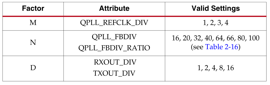
其中,N,M以及D表示QPLL分频器的属性,如下表:

QPLL的分频属性

下面是几个通用协议的QPLL分频器属性设置值,可以自行验证:
QPLL分频器属性设置

### QPLL Reset in FPGA or Communication Systems Explanation and Solution #### Understanding the Role of QPLL Reset In high-speed transceivers, such as those found within GTX/GTH components on FPGAs like xc7z030ffg676-2, ensuring proper initialization is critical for reliable operation at speeds up to 10.3125 Gb/s[^3]. The Quad PLL (QPLL) plays a significant role in providing stable clocking solutions necessary for these operations. Each GTX/GTH quad contains three dedicated ports specifically designed for resetting the QPLL: `QPLLRESET`, which serves as an input signal that triggers the reset process; and `QPLLLOCK`, acting as an output indicating when this procedure has successfully completed[^2]. #### Implementation Details To perform a successful QPLL reset: When initiating a system startup sequence involving GT transceivers utilizing QPLLs, it's essential first to assert the `QPLLRESET` line low before applying any other configuration settings. This action ensures all internal states are cleared properly prior to beginning normal functioning modes. Once initiated by setting `QPLLRESET=0`, wait until observing `QPLLLOCK`=high after releasing (`QPLLRESET`=1). Only proceed with further configurations once confirmation through `QPLLLOCK` status indicates stability post-reset completion. ```verilog // Example Verilog code snippet demonstrating how one might handle QPLL reset logic. initial begin // Assert reset initially qpllreset = 0; @(posedge clk); // Wait for rising edge of reference clock // Release reset and monitor lock status qpllreset = 1; while (!qpllock) @ (posedge clk); end ``` This approach guarantees synchronization between hardware elements involved during power-up sequences where timing-sensitive actions must occur sequentially without interference from previous operational remnants present inside registers or latches associated with the phase-locked loop circuitry. #### Common Issues and Solutions Failure scenarios related to improper handling of QPLL resets often manifest themselves via unstable link connections characterized by frequent retransmissions due to corrupted data frames over Ethernet interfaces operating near maximum throughput capacities supported by underlying physical layers configured using GTX transmitters/receivers set at higher baud rates exceeding typical CPLL limitations around ~5.9 GHz boundary points specified earlier. For troubleshooting purposes, consider verifying correct implementation details concerning assertion/deassertion timings applied against control lines responsible for managing state transitions throughout various stages comprising full-scale initialization routines executed upon device bootstrapping events triggered either manually under laboratory conditions or automatically following unexpected shutdown occurrences experienced out-in-the-field deployments relying heavily upon robustness provided by well-engineered recovery mechanisms built into modern-day programmable devices incorporating advanced serdes architectures optimized towards delivering superior performance metrics across diverse application domains spanning telecommunications infrastructure projects alongside enterprise networking equipment installations requiring deterministic latency characteristics along with minimal jitter levels achievable only through precise management practices adhered strictly according to manufacturer guidelines outlined within technical documentation accompanying specific product families targeted toward professional engineers working within relevant industries leveraging cutting-edge technologies offered today’s marketplace leaders specializing semiconductor fabrication processes yielding highly integrated circuits capable supporting multi-gigabit per second transfers reliably day-after-day year-over-year consistently meeting stringent quality assurance standards expected top-tier customers worldwide seeking best-of-breed solutions addressing their most challenging problems effectively yet efficiently balancing cost versus benefit tradeoffs inherent complex electronic designs pushing boundaries what currently possible given existing constraints imposed both physics materials science fields driving innovation forward continuously evolving landscape shaped rapidly advancing research efforts uncovering new possibilities previously thought unattainable just few short years ago but now becoming reality thanks relentless pursuit excellence demonstrated countless innovators contributing meaningful advancements benefiting society large scale transformative impacts felt far beyond initial conception phases eventually leading widespread adoption mainstream applications impacting everyday lives positively profound ways unimaginable decades past. --related questions-- 1. What are common pitfalls encountered during GTX/GTH transceiver initialization? 2. How does selecting between CPLL vs QPLL impact design choices for different speed requirements? 3. Can you provide examples of situations where incorrect QPLL reset leads to functional issues? 4. Are there alternative methods besides software-controlled resets for initializing QPLL? 5. In what scenarios would someone choose not to use QPLL despite its advantages?
评论
添加红包

请填写红包祝福语或标题

红包个数最小为10个

红包金额最低5元

当前余额3.43前往充值 >
需支付:10.00
成就一亿技术人!
领取后你会自动成为博主和红包主的粉丝 规则
hope_wisdom
发出的红包

打赏作者

李锐博恩

你的鼓励将是我创作的最大动力

¥1 ¥2 ¥4 ¥6 ¥10 ¥20
扫码支付:¥1
获取中
扫码支付

您的余额不足,请更换扫码支付或充值

打赏作者

实付
使用余额支付
点击重新获取
扫码支付
钱包余额 0

抵扣说明:

1.余额是钱包充值的虚拟货币,按照1:1的比例进行支付金额的抵扣。
2.余额无法直接购买下载,可以购买VIP、付费专栏及课程。

余额充值