


今天浅刷一下移位寄存器吧。这里鼠鼠并没有学的很好,学校里的数电考试没怎么强调这一块,刚好补一补这一块的知识捏。
107 4-bit shift register
要求设计一个异步复位、同步置数带使能功能的4位移位寄存器。输入比置数优先级更高。
一层一层写就行了。
module top_module(
    input clk,
    input areset,  // async active-high reset to zero
    input load,
    input ena,
    input [3:0] data,
    output reg [3:0] q);

    always @(posedge clk or posedge areset) begin
        if (areset)
            q<=0;
    	else begin
            if (load==1)
                q<=data;
            else begin
                if(ena==1) begin
                    q[3]<=1'b0;
                    for(int i=0;i<3;i++)
                        q[i]<=q[i+1];
                end
                else q<=q;
            end
        end
    end
endmodule
108 left/right rotator
要求设计100位的同步置数且能选择左右的旋转器。
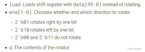
其实和106差不多,特殊情况换了一下而已。
module top_module(
    input clk,
    input load,
    input [1:0] ena,
    input [99:0] data,
    output reg [99:0] q);
    always @(posedge clk) begin
        if(load==1)
            q<=data;
        else begin
            case(ena)
                2'b01:begin
                    q[99]<=q[0];
                    for(int i=0;i<99;i++)begin
                        q[i]<=q[i+1];
                    end
                end
                2'b10:begin
                    q[0]<=q[99];
                    for(int j=99;j>0;j--)begin
                        q[j]<=q[j-1];
                    end
                end
                default:q<=q;
            endcase
        end
    end
endmodule
109 left/right arithmetic shift by 1 or 8
设计一个64位的异步置数算术移位寄存器。
这段话鼠鼠没看懂:
An arithmetic right shift shifts in the sign bit of the number in the shift register (q[63] in this case) instead of zero as done by a logical right shift. Another way of thinking about an arithmetic right shift is that it assumes the number being shifted is signed and preserves the sign, so that arithmetic right shift divides a signed number by a power of two.
There is no difference between logical and arithmetic left shifts.
不如问问智慧(x)的大模型吧:
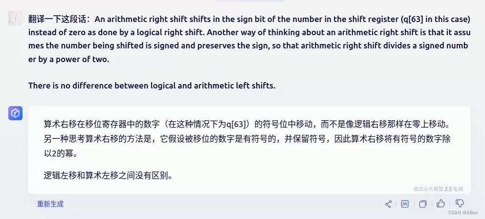
重新翻了数电ppt,貌似懂了,算术左移和逻辑左移过程一样,最低位补0,算术右移和逻辑右移操作过程不一样。
对于逻辑移位,就是不考虑符号位,移位的结果只是数据所有的位数进行移位。根据移位操作的目的,左移时,低位补0,右移时,高位补0。算术是带有符号的数据,所以我们不能直接移动所有的位数,这可能会使得符号不正确。
逻辑右移在左端补k个0,算术右移是在左端补k个最高有效位的值。在这里最高有效位就是q[63]。知道了这个就好写了。
module top_module(
    input clk,
    input load,
    input ena,
    input [1:0] amount,
    input [63:0] data,
    output reg [63:0] q);
    always @(posedge clk) begin
        if(load)
            q<=data;
        else begin
            if(ena) begin
                case(amount)
                    2'b00:q<={q[62:0],1'b0};
                    2'b01:q<={q[55:0],8'b0};
                    2'b10:q<={q[63],q[63:1]};
                    2'b11:q<={{8{q[63]}},q[63:8]};
                endcase
            end
            else q<=q;
        end
    end
endmodule
110 5-bit LFSR
线性反馈移位寄存器(LFSR,linear feedback shift register)是指仅使用一些异或门来产生下一状态的移位寄存器。
LSFR又分为两大类,分别是伽罗瓦寄存器(Galois LFSR,内部LFSR)和斐波那契寄存器。
A Galois LFSR is one particular arrangement where bit positions with a "tap" are XORed with the output bit to produce its next value, while bit positions without a tap shift. If the taps positions are carefully chosen, the LFSR can be made to be "maximum-length". A maximum-length LFSR of n bits cycles through 2n-1 states before repeating (the all-zero state is never reached).
The following diagram shows a 5-bit maximal-length Galois LFSR with taps at bit positions 5 and 3. (Tap positions are usually numbered starting from 1). Note that I drew the XOR gate at position 5 for consistency, but one of the XOR gate inputs is 0.
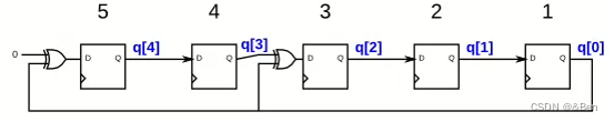
题目举出的这个例子抽头(tap)位置是5和3,也就是说,这个寄存器的抽头位的输出是最后的输出与抽头位的输入的异或。线性反馈寄存器常用于加密领域。
题目要求构建一个5位的伽罗瓦线性反馈移位寄存器,其中抽头是5和3.
module top_module(
    input clk,
    input reset,    // Active-high synchronous reset to 5'h1
    output [4:0] q
);
    always @(posedge clk)begin
        if (reset)
            q<=5'h1;
        else begin
            q[4]<=0^q[0];
            q[3]<=q[4];
            q[2]<=q[3]^q[0];
            q[1]<=q[2];
            q[0]<=q[1];
        end
    end

endmodule
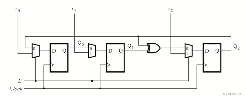
111 3-bit LFSR
要求构建一个如图的三位的LFSR。
module top_module (
	input [2:0] SW,      // R
	input [1:0] KEY,     // L and clk
	output [2:0] LEDR);  // Q

    ff ff1(.r(SW[0]),.q(LEDR[2]),.ld(KEY[1]),.clk(KEY[0]),.out(LEDR[0]));
    ff ff2(.r(SW[1]),.q(LEDR[0]),.ld(KEY[1]),.clk(KEY[0]),.out(LEDR[1]));
    ff ff3(.r(SW[2]),.q(LEDR[1]^LEDR[2]),.ld(KEY[1]),.clk(KEY[0]),.out(LEDR[2]));

endmodule

module ff(
    input r,
    input q,
    input ld,
    input clk,
    output out
);
    wire l;

    always @(posedge clk)begin
        out<=l;
    end
    always @(ld)begin
        l<=ld?r:q;
    end
endmodule
112 32-bit LFSR
题目要求构建一个32位的伽罗瓦线性反馈移位寄存器,其中抽头是32、22、2和1位。
考虑使用条件选择+循环.
module top_module(
    input clk,
    input reset,    // Active-high synchronous reset to 32'h1
    output [31:0] q
);
    always @(posedge clk)begin
        if(reset)
            q<=32'h1;
        else begin
            for(int i=0;i<32;i++)begin
                if(i!=31&&i!=21&&i!=1&&i!=0)
                    q[i]<=q[i+1];
                else if(i==31)
                    q[31]<=0^q[0];
                else if(i==21)
                    q[21]<=q[22]^q[0];
                else if(i==1)
                    q[1]<=q[2]^q[0];
                else
                    q[0]<=q[1]^q[0];
            end
        end
    end

endmodule
113 Shift register Exams/m2014 q4k
要求实现如下电路:
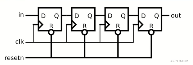
module top_module (
    input clk,
    input resetn,   // synchronous reset
    input in,
    output out);

    wire w1,w2,w3;

    dfff dff1(.in(in),.clk(clk),.resetn(resetn),.out(w1));
    dfff dff2(.in(w1),.clk(clk),.resetn(resetn),.out(w2));
    dfff dff3(.in(w2),.clk(clk),.resetn(resetn),.out(w3));
    dfff dff4(.in(w3),.clk(clk),.resetn(resetn),.out(out));


endmodule

module dfff(
    input in,
    input clk,
    input resetn,
    output out
);
    always @(posedge clk)begin
        if(!resetn)
            out<=0;
        else
            out<=in;
    end
endmodule
114 Shift register Exams/2014 q4b
要求设计如图所示的n位移位寄存器:
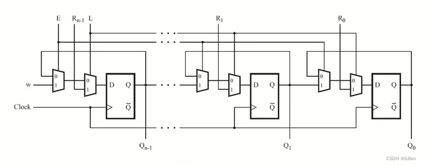
题目要求假设n=4,并且假设这个电路在DE2板上能实现。
module top_module (
    input [3:0] SW,
    input [3:0] KEY,
    output [3:0] LEDR
); //

    MUXDFF muxdff1(.e(KEY[1]),.r(SW[3]),.l(KEY[2]),.w(KEY[3]),.clk(KEY[0]),.out(LEDR[3]));
    MUXDFF muxdff2(.e(KEY[1]),.r(SW[2]),.l(KEY[2]),.w(LEDR[3]),.clk(KEY[0]),.out(LEDR[2]));
    MUXDFF muxdff3(.e(KEY[1]),.r(SW[1]),.l(KEY[2]),.w(LEDR[2]),.clk(KEY[0]),.out(LEDR[1]));
    MUXDFF muxdff4(.e(KEY[1]),.r(SW[0]),.l(KEY[2]),.w(LEDR[1]),.clk(KEY[0]),.out(LEDR[0]));

endmodule

module MUXDFF (
	input e,
    input r,
    input l,
    input w,
    input clk,
    output out
);
    reg w1,w2;

    always @(posedge clk)begin
        out<=w2;
    end

    always @(e or l)begin
        w1<=e?w:out;
        w2<=l?r:w1;
    end

endmodule
115 3-input LUT
In this question, you will design a circuit for an 8x1 memory, where writing to the memory is accomplished by shifting-in bits, and reading is "random access", as in a typical RAM. You will then use the circuit to realize a 3-input logic function.
First, create an 8-bit shift register with 8 D-type flip-flops. Label the flip-flop outputs from Q[0]...Q[7]. The shift register input should be called S, which feeds the input of Q[0] (MSB is shifted in first). The enable input controls whether to shift. Then, extend the circuit to have 3 additional inputs A,B,C and an output Z. The circuit's behaviour should be as follows: when ABC is 000, Z=Q[0], when ABC is 001, Z=Q[1], and so on. Your circuit should contain ONLY the 8-bit shift register, and multiplexers. (Aside: this circuit is called a 3-input look-up-table (LUT)).
🕐创建一个存储器:
首先,用8个D型触发器创建一个8位移位寄存器。标记触发器的输出为Q[0]…Q[7]。移位寄存器的输入应称为S,它为Q[0]的输入供电(MSB首先被移位)。输入enable控制是否移位。
然后,扩展电路以增加3个额外的输入A、B、C和一个输出Z。电路的行为应如下:当ABC为000时,Z=Q[0],当ABC为001时,Z=Q[1],以此类推。你的电路应仅包含8位移位寄存器和多路复用器。
这个电路也被称为3输入查找表。
🕑MSB:Most Significant Bit ,最高有效位。在二进制中,最高有效位位最高加权位,一般位于最左侧。
🕒查找表:look-up-table,是一种用于替代复杂计算的数据结构,可以加速查询操作。它本质上是一个数组,通常用于实现非线性函数或者映射关系。查找表通常预先计算并存储可能的结果,使用时直接查表获取结果,而不需要进行复杂的计算。这样可以大大提高查询速度,同时减少计算资源的消耗。在数字信号处理、图像处理、计算机图形学等领域,查找表被广泛应用。
module top_module (
    input clk,
    input enable,
    input S,
    input A, B, C,
    output Z );

    reg [7:0] q;
    always @(posedge clk)
        begin
            if(enable)begin
                q <= {q[6:0],S};
            end
            else begin
                q <= q;
            end
        end
    assign Z = q[{A,B,C}];

endmodule
终于肝完移位寄存器了。。。。。。。


 4万+
4万+


 被折叠的 条评论
为什么被折叠?
被折叠的 条评论
为什么被折叠?
 到【灌水乐园】发言


